EP1341184B1 - Speicheranordnung mit kohlenstoffnanoröhre und Verfahren zur Herstellung der Speicheranordnung - Google Patents
Speicheranordnung mit kohlenstoffnanoröhre und Verfahren zur Herstellung der Speicheranordnung Download PDFInfo
- Publication number
- EP1341184B1 EP1341184B1 EP03250805A EP03250805A EP1341184B1 EP 1341184 B1 EP1341184 B1 EP 1341184B1 EP 03250805 A EP03250805 A EP 03250805A EP 03250805 A EP03250805 A EP 03250805A EP 1341184 B1 EP1341184 B1 EP 1341184B1
- Authority
- EP
- European Patent Office
- Prior art keywords
- carbon nanotube
- film
- memory device
- charge storage
- insulating film
- Prior art date
- Legal status (The legal status is an assumption and is not a legal conclusion. Google has not performed a legal analysis and makes no representation as to the accuracy of the status listed.)
- Expired - Fee Related
Links
Images


Classifications
-
- G—PHYSICS
- G11—INFORMATION STORAGE
- G11C—STATIC STORES
- G11C13/00—Digital stores characterised by the use of storage elements not covered by groups G11C11/00, G11C23/00, or G11C25/00
- G11C13/02—Digital stores characterised by the use of storage elements not covered by groups G11C11/00, G11C23/00, or G11C25/00 using elements whose operation depends upon chemical change
- G11C13/025—Digital stores characterised by the use of storage elements not covered by groups G11C11/00, G11C23/00, or G11C25/00 using elements whose operation depends upon chemical change using fullerenes, e.g. C60, or nanotubes, e.g. carbon or silicon nanotubes
-
- B—PERFORMING OPERATIONS; TRANSPORTING
- B82—NANOTECHNOLOGY
- B82Y—SPECIFIC USES OR APPLICATIONS OF NANOSTRUCTURES; MEASUREMENT OR ANALYSIS OF NANOSTRUCTURES; MANUFACTURE OR TREATMENT OF NANOSTRUCTURES
- B82Y10/00—Nanotechnology for information processing, storage or transmission, e.g. quantum computing or single electron logic
-
- G—PHYSICS
- G11—INFORMATION STORAGE
- G11C—STATIC STORES
- G11C2213/00—Indexing scheme relating to G11C13/00 for features not covered by this group
- G11C2213/10—Resistive cells; Technology aspects
- G11C2213/17—Memory cell being a nanowire transistor
-
- Y—GENERAL TAGGING OF NEW TECHNOLOGICAL DEVELOPMENTS; GENERAL TAGGING OF CROSS-SECTIONAL TECHNOLOGIES SPANNING OVER SEVERAL SECTIONS OF THE IPC; TECHNICAL SUBJECTS COVERED BY FORMER USPC CROSS-REFERENCE ART COLLECTIONS [XRACs] AND DIGESTS
- Y10—TECHNICAL SUBJECTS COVERED BY FORMER USPC
- Y10S—TECHNICAL SUBJECTS COVERED BY FORMER USPC CROSS-REFERENCE ART COLLECTIONS [XRACs] AND DIGESTS
- Y10S977/00—Nanotechnology
- Y10S977/902—Specified use of nanostructure
- Y10S977/932—Specified use of nanostructure for electronic or optoelectronic application
- Y10S977/943—Information storage or retrieval using nanostructure
Definitions
- the present invention relates to a memory device and a method of fabricating the same, and more particularly, to a memory device including a carbon nanotube which serves as a charge moving channel and a method of fabricating the memory device.
- Semiconductor memory devices fundamentally include a capacitor which preserves stored charges and a transistor which serves as a switch for securing a path of current necessary to write data to or read data from the capacitor.
- MOSFETs metal oxide filed effect transistors
- MOSFETs basically include gate electrodes made of doped polycrystalline silicon and source and drain electrodes made of doped crystalline silicon.
- the transconductance of MOSFETs is inversely proportional to the length (L) of a channel, the thickness of a gate oxide film, or the like, and is directly proportional to a surface mobility, the permittivity of the gate oxide film, and the width (W) of the channel. Since the surface mobility and the permittivity of the gate oxide film are predetermined by a directional silicon wafer, a silicon oxide film, and the like, a high transconductance can be obtained by increasing a W/L ratio of the channel or thinning the gate oxide film.
- a reduction of the sizes of source and drain electrodes includes a reduction of the thicknesses thereof, that is, junction depths, creating a larger electrical resistance. Also, a reduction in the distance between a source and a drain sometimes causes a punch through, in which a source and a depletion layer of a drain come in contact with each other, making it impossible to adjust current. In addition, such a reduction in the size of a memory device causes the width of a channel serving as a current path to be reduced to 70nm or less, preventing a smooth flow of current. Consequently, the memory device malfunctions.
- MOSFETs general memory devices based on MOSFETs are not suitable for use as future high-density memory because of problems, such as, heat loss, great power consumption, an electrical characteristic variation, charge leakage, and the like.
- a carbon nanotube memory device including a substrate, a source electrode, a drain electrode, a carbon nanotube, a memory cell, and a gate electrode.
- the source electrode and the drain electrode are arranged with predetermined interval between them on the substrate and subjected to a voltage.
- the carbon nanotube connects the source electrode to the drain electrode and serves as a channel for charges.
- the memory cell is located over the carbon nanotube, and stores charges from the carbon nanotube.
- the gate electrode is formed in contact with the upper surface of the memory cell and controls the amount of charge flowing from the carbon nanotube into the memory cells.
- the present invention provides a fast, highly-integrated memory device which prevents an increase in resistance due to miniaturization of the memory device, and provides a low thermal loss, a low power consumption, stable electrical characteristics, and a low charge leakage.
- the substrate may be formed of silicon, and a silicon oxide film may be deposited on the substrate.
- the memory cell may include: a first insulating film formed in contact with the upper surface of the carbon nanotube; a charge storage film, deposited on the first insulating film, that stores charges; and a second insulating film formed on the charge storage film and contacting the gate electrode.
- the thickness of the first insulating film is similar to the thickness of the charge storage film, for example within 25% or preferably 10% of its value, and the thickness of the second insulating film is approximately double the thickness of the charge storage film, for example within 25%, or preferably 10%, of double the value.
- the first and second insulating films may be formed of silicon oxide, and the charge storage film may be formed of one of silicon and silicon nitride.
- the charge storage film has a thickness of 15nm or less
- the charge storage film can be a porous film having a plurality of nanodots filled with a charge storage material.
- the memory cell may include: a third insulating film formed in contact with the lower surface of the gate electrode; and a porous film deposited below the third insulating film, in contact with the carbon nanotube, the porous film having a plurality of nanodots filled with the charge storage material.
- the thickness of the third insulating film may be approximately double the thickness of the porous film or be similar to the thickness of the porous film, again, for example, within 25% or preferably 10% of its value or double its value.
- the third insulating film may be formed of silicon oxide, and the charge storage material may be one of silicon and silicon nitride.
- the porous film may be made of aluminum oxide.
- a nanodot has a diameter of 15nm or less.
- a method of fabricating a carbon nanotube memory device including the following three steps.
- a carbon nanotube grows on a substrate, and a source electrode and a drain electrode are formed in contact with the carbon nanotube such that the carbon nanotube between the source electrode and the drain electrode serves as a charge moving channel.
- a memory cell is formed in contact with the carbon nanotube, by sequentially depositing a first insulating film, a charge storage film, and a second insulating film on the carbon nanotube, the source electrode, and the drain electrode, and patterning the resultant structure using a photolithographic method.
- a gate electrode which controls the amount of charge flowing from the carbon nanotube into the charge storage film is formed by depositing a metal layer on the second insulating film and patterning the resultant structure using a photolithographic method.
- an insulating layer is first formed on the upper surface of the substrate, and then the carbon nanotube is grown on the upper surface of the insulating layer.
- the substrate may be formed of silicon
- the insulating layer may be formed of silicon oxide.
- the source and drain electrodes may be formed by e-beam lithography.
- the first insulating film is deposited to a thickness similar to the thickness of the charge storage film, for example within 25% or preferably 10% of its value, and the second insulating film is deposited to a thickness approximately double the thickness of the charge storage film, for example within 25% or preferably 10% of double its value.
- the first and second insulating films may be formed of silicon oxide, and the charge storage film may be formed of one of silicon and silicon nitride.
- the charge storage film has a thickness of 15nm or less.
- a method of fabricating a carbon nanotube memory device including the following five steps.
- a carbon nanotube grows on a substrate, and a source electrode and a drain electrode are formed in contact with the carbon nanotube such that the carbon nanotube between the source electrode and the drain electrode serves as a charge moving channel.
- a porous film having a plurality of nanodots is formed by depositing a first insulating film on the upper surfaces of the carbon nanotube and the source and drain electrodes, and anode-oxidizing and etching the first insulating film.
- the nanodots are filled with a charge storage material, by depositing the charge storage material on the upper surface of the porous film and then etching the charge storage material.
- a memory cell is formed by depositing a second insulating film on the upper surface of the porous film and patterning the first insulating film, the porous film, and the second insulating film using a photolithographic method.
- a gate electrode which controls the amount of charge flowing from the carbon nanotube into the charge storage film is formed by depositing a metal layer on the second insulating film and patterning the resultant structure using a photolithographic method.
- an insulating layer is formed on the upper surface of the substrate, and the carbon nanotube is grown on the upper surface of the insulating layer.
- the substrate may be formed of silicon
- the insulating layer may be formed of silicon oxide.
- the source and drain electrodes may be formed by e-beam lithography.
- the first insulating film is deposited to a thickness similar to the thickness of the porous film, for example within 25% or preferably 10% of its value, and the second insulating film is deposited to a thickness approximately double the thickness of the porous film, for example within 25% or preferably 10% of double its value.
- the first and second insulating films may be formed of silicon oxide, and the charge storage film may be formed of one of silicon and silicon nitride.
- the porous film is formed to a thickness of 15nm or less.
- the entire first insulating film may be oxidized to form the porous film having the plurality of nanodots.
- the memory device because a carbon nanotube is used as a charge moving channel, a doping process for a semiconductor memory device may not be required. Furthermore, because a carbon nanotube having a high electrical conductivity and a high thermal conductivity is used, an increase in resistance and malfunction due to the high-integration of a memory device are prevented. Also, because the memory device according to the present invention includes the charge storage film to store charge, or a porous film having nanodots, the memory device functions as a highly efficient, highly-integrated memory device.
- a memory device includes a substrate 11, an insulating layer 13 deposited on the substrate 11, a source electrode 15 and a drain electrode 17 which are made of metal and isolated a predetermined distance from each other on the insulating layer 13, a carbon nanotube 21 which connects the source electrode 15 to the drain electrode 17 and serves as an electron moving channel, a memory cell 23 which contacts the carbon nanotube 21 and stores charges of electrons (or holes), and a gate electrode 19 which contacts the memory cell 23 and controls the motion of the electrons.
- the source and drain electrodes 15 and 17 are installed on the substrate 11. However, the source and drain electrodes 15 and 17 may be installed within the substrate 11. In this case, the carbon nanotube 21 is also located within the substrate 11, or installed in contact with the inner surface of the substrate 11.
- the substrate 11 is generally made of silicon, and the insulating layer 13 formed on the substrate 11 is made of silicon oxide.
- the source and drain electrodes 15 and 17 may be formed of a metal such as titanium (Ti) or gold (Au).
- the gate electrode 19 may be formed of a metal such as polysilicon.
- the transistor structure is formed by well-known semiconductor processes, such as, photolithography, e-beam lithography, etching, oxidation, and thin film deposition.
- the carbon nanotube 21 is a carbon allotrope having a honeycomb shape formed by combining carbon atoms with one another.
- the carbon nanotube 21 has a shape in which a graphite sheet formed by a combination of a plurality of carbon atoms is rolled in a circle with a nano-sized diameter.
- the carbon nanotube 21 has either metal properties or semiconductor properties depending on the rolling angle and structure of the graphite sheet. These characteristics of a carbon nanotube are being actively studied in up-to-date industrial fields, particularly, in the field of nano-technology.
- Carbon nanotubes are classified into two different types according to their electrical properties.
- One type is metallic carbon nanotubes whose electronic behavior is ohmic and unaffected by a gate voltage.
- the other type is semiconductor carbon nanotubes whose electronic behavior is non-ohmic and affected by a gate voltage.
- the carbon nanotube 21 used in the memory device according to the embodiment of the present invention is a semiconductor carbon nanotube.
- a flow of electrons moving through the carbon nanotube 21, that is, current, is controlled by varying a voltage applied to the gate electrode 19.
- the carbon nanotube 21 can be manufactured by arc discharge, laser vaporization, plasma enhanced chemical vapor deposition (PECVD), thermal chemical vapor deposition, vapor phase growth, or the like.
- PECVD plasma enhanced chemical vapor deposition
- thermal chemical vapor deposition thermal chemical vapor deposition, vapor phase growth, or the like.
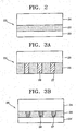
- FIGS. 2, 3A, and 3B First, second, and third memory cells 23, 25, and 35 used in a memory device according to an embodiment of the present invention are shown in FIGS. 2, 3A, and 3B, respectively.
- the first memory cell 23 used in the memory device according to an embodiment of the present invention indudes first and second insulating films 20 and 24 and a charge storage film 22.
- the charge storage film 22 stores charges, that is to say, electrons or holes, and is interposed between the first and second insulating films 20 and 24.
- the first and second insulating films 20 and 24 are formed of silicon oxide SiO 2
- the charge storage film 22 is formed of silicon (Si) or silicon nitride (Si 3 N 4 ).
- a Si 3 N 4 thin film is provided as a low-potential trap site which can store a plurality of charges.
- the thickness of the entire first memory cell 23 is about 60nm, and the thickness of the charge storage film 22 is about 15nm or less. It was confirmed that a silicon film or a silicon nitride film used as the charge storage film 22 was able to store electrons when it had a thickness of 100nm or less.
- the first insulating film 20 is thin enough that charges received from the carbon nanotube 21 of FIG. 1 can easily tunnel, and the second insulating film 24 is thick enough to prevent charges from the gate electrode 19 from being introduced thereinto and preserve charges stored in the charge storage film 22 for a long time.
- the first insulating film 20 is a 7nm oxide thin film
- the charge storage film 22 is a 7nm Si 3 N 4 thin film
- the second insulating film 24 is a 14nm oxide thin film.
- the first insulating film 20, the charge storage film 22, and the second insulating film 24 are formed to have a thickness ratio of 1:1:2 so that charges from the carbon nanotube 21 can be stably stored in the charge storage film 22 for a long time.
- FIG. 3A is a cross section of the second memory cell 25 adopted in a memory device according to an embodiment of the present invention.
- the second memory cell 25 includes a third insulating film 29 formed in contact with the gate electrode 19, and a porous film 26 which is formed below the third insulating film 29 and has a plurality of nanodots 27 filled with a charge storage material 28.
- the third insulating film 29 can be formed of silicon oxide, and the charge storage material 28 can be silicon or silicon nitride.
- the third insulating film 29 is thicker than the porous film 26 so as to stably store the charge storage material 28 in the nanodots 27.
- FIG. 3B is a cross section of the third memory cell 35 adopted in a memory device according to an embodiment of the present invention.
- the third memory cell 35 has a structure in which an insulating film is further formed below the porous film 26 of the second memory cell 25.
- the third memory cell 35 includes a fourth insulating film 34, a porous film 36 having a plurality of nanodots 37 filled with a charge storage material 38, and a fifth insulating film 34'.
- the fourth insulating film 34 is thick enough to prevent charges from the gate electrode 19 of FIG. 1 from being introduced thereinto and preserve charges stored in the charge storage film 38 for a long time.
- the fifth insulating film 34' is thin enough that electrons or holes from the carbon nanotube 21 can easily tunnel therethrough and move into the porous film 36.
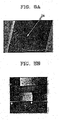
- FIG. 4 is a scanning electron microscopy (SEM) picture of the third memory cell 35 adopted in a memory device according to an embodiment of the present invention.
- the fourth insulating film 34 is formed of SiO 2
- the porous film 36 and the third insulating film 34' are formed of Al 2 O 3
- the charge storage material 38 is formed of Si (or Si 3 N 4 ).
- FIGS. 5A and 5B are SEM pictures showing the carbon nanotube 21 which connects the source electrode 15 to the drain electrode 17 in a memory device according to an embodiment of the present invention. Using an atomic energy microscopy, the carbon nanotube 21 was measured to have a diameter of about 3nm.
- FIGS. 6A through 6I are perspective views for illustrating a method of manufacturing a memory device according to an embodiment of the present invention employing the first memory cell 23.
- the insulating layer 13 is deposited on the upper surface of the substrate 11, and the carbon nanotube 21 then grows on the insulating layer 13.
- Carbon nanotube (CNT) powder created by CVD is scattered into a chloroform solution and then coated and dried at several places over the insulating layer 13.
- FIG. 6A shows a single carbon nanotube 21 formed at one place on the substrate 11.
- a conductive material layer 14 for forming the source and drain electrodes 15 and 17 is deposited on the insulating layer 13, and a mask 12a is then used to pattern the conductive material layer 14 by e-beam lithography.
- the conductive material layer 14 can be formed of a metal, such as, Au or Ti.
- the source and drain electrodes 15 and 17 formed after the mask patterning are thermally annealed to reduce contact resistance.
- the source and drain electrodes 15 and 17 can be quickly annealed at 600 °C for about 30 seconds. The source and drain electrodes 15 and 17 formed in this way are shown in FIG. 6C.
- FIGS. 6D through 6F illustrate a process of depositing the first memory cell 23.
- a first insulating film 20a, a charge storage film 22a, and a second insulating film 24a are sequentially deposited on the source and drain electrodes 15 and 17, on the carbon nanotube 21 connecting the source electrode 15 to the drain electrode 17, and on the insulating layer 13, thereby forming a memory cell 23a.
- a mask 12b is positioned over the resultant structure of FIG. 6D, and exposed to light, and then the resulting structure is developed.
- the first memory cell 23 is formed in contact with the upper surface of the source and drain electrodes 15 and 17 and the upper surface of the carbon nanotube 21.
- the first memory cell 23 includes a first insulating film 20 made of oxide, a charge storage film 22 made of Si or Si 3 N 4 , and a second insulating film 24 made of oxide.
- An oxide film is formed by CVD using a mixture of SiH4 gas and O 2 gas, and a Si 3 N 4 film is formed by CVD using SiH 2 Cl 2 gas and NH 3 gas.
- FIGS. 6G through 6I illustrate a process of forming the gate electrode 19.
- a metal layer 18 for forming the gate electrode 19 is deposited on the insulating layer 13 to cover the carbon nanotube 21 and the first memory cell 23.
- a mask 12c is positioned over the metal layer 18 and then exposed to ultraviolet, and then the resultant structure is developed.
- the gate electrode 19 is formed as shown in FIG. 61.
- FIGS. 7A through 7E illustrate a method of manufacturing the third memory cell 35 adopted in a memory device according to an embodiment of the present invention.
- the fifth insulating film 34' is oxidized to obtain an oxide film 36' thereon.
- the porous film 36 having the plurality of nanodots 37 is made as shown in FIG. 7B.
- the fifth insulating film 34' is formed of aluminium, the aluminium is dipped into a sulphuric acid solution or a phosphoric acid solution and oxidized using electricity to form the plurality of nanodots 37. This oxidization is referred to as anodization.
- the aluminium is oxidized to turn it into alumina, which has a larger volume than the original aluminium.
- the nanodots 37 are filled with silicon or silicon nitride, the material of the charge storage film 22, using CVD or a sputtering technique. Thereafter, as shown in FIG. 7D, the resultant nanodots 37 are dry-etched to form the porous film 36 which can collect charges. Then, as shown in FIG. 7E, the fourth insulating film 34 is deposited on the porous film 36, thereby completing the fabrication of the third memory cell 35.
- the carbon nanotube 21 and the source and drain electrodes 15 and 17 are formed as shown in FIGS. 6A through 6C.
- the third memory cell 35 can be formed on the carbon nanotube 21 as shown in FIGS. 7A through 7E. Thereafter, as shown in FIGS. 6G through 61, the gate electrode 19 can be formed.
- the second memory cell 25 can be formed in a similar way to the fabrication method of the third memory cell 35.
- the porous film 26 having the plurality of nanodots 27 is formed by completely oxidizing the fifth insulating film 34'. Thereafter, the nanodots 27 are filled with the charge storage material 28, and the third insulating film 29 is then deposited on the resultant porous film 26, thereby forming the second memory cell 25 of FIG. 3A.
- a memory device In a memory device according to an embodiment of the present invention, if the source electrode 15 is grounded, and a positive drain voltage is applied to the drain electrode 17, electrons move to the carbon nanotube 21, so that current flows. At this time, if a predetermined gate voltage higher than the drain voltage applied to the drain electrode 17 is applied to the gate electrode 19, electrons from the carbon nanotube 21 move to the memory cell (23, 25, or 35), tunnel through the first insulating film 20 or the fifth insulating film 34', and move to the charge storage film 22 or the nanodots 27 and 37.
- the gate and drain voltages electrons are stored in, erased from, and flow out of the charge storage film 22 and the nanodots 27 and 37, thereby achieving data recording, removal, and reproduction.
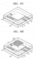
- FIG. 8A is a plan view of a memory device according to an embodiment of the present invention including a single gate electrode, and a plurality of source and drain electrodes and a carbon nanotube that are located under the gate electrode.
- FIG. 8B is a picture showing a carbon nanotube channel connecting a source electrode (S) and a drain electrode (D) of FIG. 8A.
- a memory device can operate as a volatile or nonvolatile memory by adequately controlling the material and thickness of the storage film for the memory cell, the diameter and length of each of the plurality of nanodots included in the porous film, the material filling the nanotube channel, the gate voltage, and the source-drain voltage.
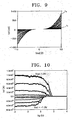
- FIG. 9 is a graph of a current Isd between a source electrode and a drain electrode versus a Vsd between the source electrode and the drain electrode when a gate voltage varies from 0V to 10V in a memory device according to an embodiment of the present invention.
- Graph f 1 shows that when the gate voltage is 0V, the source-drain current I sd is 0 regardless of a variation in the source-drain voltage V sd .
- Graph f 2 shows that when the gate voltage is 10V, the source-drain current I sd increases from 0 to about 1000nA as the source-drain voltage V sd increases from 0 to a positive value, but the source-drain current I sd decreases from 0 to about -1000nA as the source-drain voltage V sd decreases from 0 to a negative value.
- the gate voltage is 0V at a certain source-drain voltage, no electrons move between a source electrode and a drain electrode, so that data writing cannot be achieved. If the gate voltage is greater than 0V, the source-drain current starts flowing. With an increase in the gate voltage, data storage can be achieved by seizing a predetermined number of electrons.
- FIG. 10 is a graph of a current Isd between a source electrode and a drain electrode versus a gate voltage Vg in a p-type CNT field effect transistor (FET) having a charge storage film which is a 28nm ONO thin film.
- FET field effect transistor
- the source-drain current Isd increases with an increase in the negative voltage of the gate electrode, and decreases to several femto ampere (fA) when the voltage of the gate electrode is positive.
- fA femto ampere
- a ratio of an on-state current Ion to an off-state current loff, lon/loff, exceeds 10 5 at Vsd 1V, when the voltage of the gate electrode varies from -4V to 4V.
- the off-state current was measured to be maintained at several pA or less. It is considered that the maintenance of the off-state current at a low value is caused by the position of the gate electrode in the memory device and a high breakdown voltage of the ONO thin film.
- a threshold voltage increases with an increase in the ratio lon/loff, thus improving performance.
- FIG. 11A shows the current-voltage (I-V) characteristics of a P-type CNT memory device including a 7nm-thick memory cell (SiO 2 /Si 3 N 4 /SiO 2 ).
- FIG. 11B shows the I-V characteristics of an N-type CNT memory device including a 30nm-thick memory cell (SiO 2 /Si 3 N 4 /SiO 2 ).
- the drain current Id in the P-type CNT memory device varies slightly with respect to the source-drain voltage Vsd. However, if the gate voltage Vg is about 2.5V, the drain current Id sharply decreases.
- FIG. 12 is a graph of a drain current Id versus a gate voltage Vg, from 0V to 1V, when different source-drain voltages Vsd are applied in an N-type CNT memory device.
- n1 denotes the case when Vsd is 0V
- n2 denotes the case when Vsd is -5V
- n3 denotes the case when Vsd is -5.5V
- n4 denotes the case when Vsd is -6V
- n5 denotes the case when Vsd is -6.5V.
- the drain current Id increases as the gate voltage Vg increases, and is saturated at about 0.6V.
- Equation 1 C/L • 2 ⁇ ⁇ ⁇ 0 /1n(2h/r)
- the above hole mobility ( ⁇ h ) is greater than the hole mobility of a single wall nanotube or the hole mobility of a multi wall nanotube (MWNT).
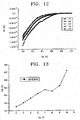
- FIG. 13 is a graph of a threshold voltage Vth versus a gate voltage Vg when a drain current Id is constantly 50nA, in a memory device according to an embodiment of the present invention.
- the threshold voltage Vth increases, which means that holes from the carbon nanotube are injected into an ONO thin film and fill a trap site.
- the threshold voltage increases by about 60mV and accordingly holes are found to be quasi-quantized.
- FIG. 14 shows a schematic diagram of an electric field between a carbon nanotube and a gate electrode and a graph of the surface induced charge density ( ⁇ ) at the gate electrode versus a distance between the CNT and the gate electrode in a memory device according to an embodiment of the present invention.
- a gate voltage forms a strong electric field around the surface of the carbon nanotube (CNT).
- the gate electrode is considered as a complete conductor, and the diameter of the CNT is 3nm, an ONO thin film between the CNT and the gate electrode can be regarded as a single layer with an effective dielectric constant of 3.
- the electric field around the CNT can be calculated. If the gate voltage is 5V, the calculated electric field is 970V/ ⁇ m, a strong field enough to induce a Fowller Nodheim tunneling.
- tunneling charges flow along electric field lines, they are trapped in a nitride thin film in proportional to the intensity of the electrical field calculated based on an induced charge distribution.
- 70% of the entire tunneling charges corresponds to the full width at half maximum (FWHW) of the peak value of a charge density, and can flow into the nitride thin film with a 14nm thickness included in the ONO thin film. It is known that charges are quantized at a room temperature when the size of a quantum dot is equal to or less than 10nm. Referring to the graph of FIG. 14, an induced charge density ( ⁇ ) increases with proximity to the CNT.
- FIG. 15 is a graph of a drain current Id versus time, for 100 seconds, in a memory device according to an embodiment of the present invention.
- a localized charge distribution enables charges to be induced into the nitride film of the ONO thin film due to a high electrical field distribution of a localized carbon nanotube, and charges trapped in localized areas of the ONO thin film can be dispersed into areas where no charges are stored.
- the entire amount of current remains constant over time. Accordingly, it can be known that a charged trap site of the ONO thin film of the CNT memory device according to the present invention serves as a quantum dot of a flash memory device.
- the present invention provides a non-volatile memory device using the CNT-FET and the ONO thin film, in which charges are stored in a trap site of the ONO thin film.
- the stored charges have a quantized voltage increment of about 60mV, which means that the ONO thin film has a quasi-quantized energy state.
- the quantized energy state is related to a high localized electric field associated with a nano-scale CNT channel and represents that a CNT memory device functions as an ultrahigh-density large-capacity flash memory.
- a memory device uses a carbon nanotube instead of an implantation channel to move charges between a source and a drain, and includes a charge storage film or a porous film having nanodots without need of an extra capacitor.
- the carbon nanotube having high electrical conductivity and high heat conductivity is used as an electron moving channel, a small transistor can be fabricated, thus enabling the fabrication of a highly-integrated, highly-efficient memory device.
- a memory device includes a small transistor which uses a highly conductive CNT and a memory cell which stores electrons, thereby providing high efficiency and high integration.
Claims (30)
- Speicheranordnung mit Kohlenstoffnanoröhre umfassend:ein Substrat (11);eine Sourceelektrode (15) und eine Drainelektrode (17), die mit einem bestimmten Intervall dazwischen auf dem Substrat (11) angeordnet sind; eine Kohlenstoffnanoröhre (21), die die Sourceelektrode (15) mit der Drainelektrode (17) verbindet und als Kanal für Ladungen dient;eine Speicherzelle (23), die über der Kohlenstoffnanoröhre (21) gelegen ist, die Ladungen von der Kohlenstoffnanoröhre (21) speichert; undeine Gateelektrode (19), die in Kontakt mit der Oberseite der Speicherzelle (23) ausgebildet ist, um die Menge an Ladung zu steuern, die von der Kohlenstoffnanoröhre (21) in die Speicherzelle (23) fließt.
- Speicheranordnung mit Kohlenstoffnanoröhre nach Anspruch 1, worin die Source- und Drainelektrode (15), (17) einer Spannung ausgesetzt sind.
- Speicheranordnung mit Kohlenstoffnanoröhre nach Anspruch 1 oder 2, worin das Substrat (11) aus Silicium gebildet ist.
- Speicheranordnung mit Kohlenstoffnanoröhre nach einem der Ansprüche 1-3, worin ein Siliciumoxidfilm auf dem Substrat (11) abgeschieden ist.
- Speicheranordnung mit Kohlenstoffnanoröhre nach einem der vorhergehenden Ansprüche, worin die Speicherzelle (23) umfasst:einen ersten Isolierfilm (20) ausgebildet in Kontakt mit der Oberseite der Kohlenstoffnanoröhre;einen Ladungsspeicherfilm (22) abgeschieden auf dem ersten Isolierfilm (20), der Ladung speichert; undeinen zweiten Isolierfilm (24) ausgebildet auf dem Ladungsspeicherfilm (22) und in Kontakt mit der Gateelektrode (19).
- Speicheranordnung mit Kohlenstoffnanoröhre nach Anspruch 5, worin die Dicke des ersten Isolierfilms (20) ähnlich der Dicke des Ladungsspeicherfilms (22) ist.
- Speicheranordnung mit Kohlenstoffnanoröhre nach Anspruch 5 oder 6, worin die Dicke des zweiten Isolierfilms (24) ungefähr das Doppelte der Dicke des Ladungsspeicherfilms (22) ist.
- Speicheranordnung mit Kohlenstoffnanoröhre nach einem der Ansprüche 5-7, worin der erste und zweite Isolierfilm (20), (24) aus Siliciumoxid gebildet sind.
- Speicheranordnung mit Kohlenstoffnanoröhre nach einem der Ansprüche 5-8, worin der Ladungsspeicherfilm (22) aus Silicium oder Siliciumnitrid gebildet ist.
- Speicheranordnung mit Kohlenstoffnanoröhre nach einem der Ansprüche 5-9, worin der Ladungsspeicherfilm (22) eine Dicke von 15 nm oder weniger aufweist.
- Speicheranordnung mit Kohlenstoffnanoröhre nach einem der Ansprüche 5-10, worin der Ladungsspeicherfilm (22) ein poröser Film ist mit einer Mehrzahl von Nanodots (27) gefüllt mit einem Ladungsspeichermaterial (28).
- Speicheranordnung mit Kohlenstoffnanoröhre nach einem der Ansprüche 1-4, worin die Speicherzelle (23) umfasst:einen dritten Isolierfilm (29) ausgebildet in Kontakt mit der Unterseite der Gateelektrode (19); undeinen unter dem dritten Isolierfilm (29) abgeschiedenen porösen Film (36), in Kontakt mit der Kohlenstoffnanoröhre (21), wobei der poröse Film (36) eine Mehrzahl von Nanodots (27) aufweist, die mit dem Ladungsspeichermaterial (28) gefüllt sind.
- Speicheranordnung mit Kohlenstoffnanoröhre nach Anspruch 12, worin die Dicke des dritten Isolierfilms (29) ungefähr das Doppelte der Dicke des porösen Films (26) ist.
- Speicheranordnung mit Kohlenstoffnanoröhre nach Anspruch 12, worin die Dicke des dritten Isolierfilms (29) ähnlich der Dicke des porösen Films (26) ist.
- Speicheranordnung mit Kohlenstoffnanoröhre nach einem der Ansprüche 12-14, worin der dritte Isolierfilm (29) aus Siliciumoxid gebildet ist.
- Speicheranordnung mit Kohlenstoffnanoröhre nach einem der Ansprüche 11-15, worin das Ladungsspeichermaterial (28) Silicium oder Siliciumnitrid ist.
- Speicheranordnung mit Kohlenstoffnanoröhre nach einem der Ansprüche 11-16, worin der poröse Film (26) aus Aluminiumoxid gebildet ist.
- Speicheranordnung mit Kohlenstoffnanoröhre nach einem der Ansprüche 11-17, worin ein Nanodot einen Durchmesser von 15 nm oder weniger aufweist.
- Verfahren zur Herstellung einer Speicheranordnung mit Kohlenstoffnanoröhre, wobei das Verfahren umfasst:(a) Züchten einer Kohlenstoffnanoröhre (21) auf einem Substrat (11) und Ausbilden einer Sourceelektrode (15) und einer Drainelektrode (17) in Kontakt mit der Kohlenstoffnanoröhre (21) derart, dass die Kohlenstoffnanoröhre (21) zwischen der Sourceelektrode (15) und der Drainelektrode (17) als Ladungsverschiebungskanal dient;(b) Ausbilden einer Speicherzelle (23) in Kontakt mit der Kohlenstoffnanoröhre (21), indem nacheinander abgeschieden werden: ein erster Isolierfilm (20), ein Ladungsspeicherfilm und ein zweiter Isolierfilm (24) auf der Kohlenstoffnanoröhre (21), der Sourceelektrode (15) und der Drainelektrode (17), und Mustern der erhaltenen Struktur unter Verwendung eines Photolithographieverfahrens; und(c) Ausbilden einer Gateelektrode (19), die die Menge an Ladung steuert, die von der Kohlenstoffnanoröhre (21) in den Ladungsspeicherfilm (22) fließt, durch Abscheiden einer Metallschicht auf dem zweiten Isolierfilm (24) und Mustern der erhaltenen Struktur unter Verwendung eines Photolithographieverfahrens.
- Verfahren nach Anspruch 19, worin der Ladungsspeicherfilm (22) eine Dicke von 15 nm oder weniger aufweist.
- Verfahren nach Anspruch 19, worin Ausbilden des Ladungsspeicherfilms (22) umfasst:(b1) Ausbilden eines porösen Films (26) mit einer Mehrzahl von Nanodots (27) durch Anodenoxidieren und Ätzen des ersten Isolierfilms (20); und(b2) Füllen der Nanodots (27) mit einem Ladungsspeichermaterial (28), indem das Ladungsspeichermaterial (28) auf der Oberseite des porösen Films (26) abgeschieden und dann das Ladungsspeichermaterial (28) geätzt wird.
- Verfahren nach Anspruch 21, worin der poröse Film (26) auf eine Dicke von 100 nm oder weniger ausgebildet wird.
- Verfahren nach Anspruch 21 oder 22, worin in Schritt (b1) der gesamte erste Isolierfilm (20) oxidiert wird, so dass der poröse Film (26) mit einer Mehrzahl von Nanodots (27) ausgebildet wird.
- Verfahren nach einem der Ansprüche 19-23, worin in Schritt (a) eine Isolierschicht (13) auf der Oberseite des Substrats (11) ausgebildet wird und die Kohlenstoffnanoröhre (21) auf der Oberseite der Isolierschicht (13) gezüchtet wird.
- Verfahren nach einem der Ansprüche 19-24, worin das Substrat (11) aus Silicium gebildet wird, und die Isolierschicht (13) aus Siliciumoxid gebildet wird.
- Verfahren nach einem der Ansprüche 19-25, worin in Schritt (a) die Source- und Drainelektrode (15), (17) durch Elektronenstrahllithographie ausgebildet werden.
- Verfahren nach einem der Ansprüche 19-26, worin in Schritt (b) der erste Isolierfilm (20) auf eine Dicke ähnlich der Dicke des Ladungsspeicherfilms (22) abgeschieden wird.
- Verfahren nach einem der Ansprüche 19-26, worin in Schritt (b) der zweite Isolierfilm (24) auf eine Dicke ähnlich dem Doppelten der Dicke des Ladungsspeicherfilms (22) abgeschieden wird.
- Verfahren nach einem der Ansprüche 19-28, worin der erste und zweite Isolierfilm (20), (24) aus Siliciumoxid gebildet werden.
- Verfahren nach einem der Ansprüche 19-29, worin der Ladungsspeicherfilm (22) aus Silicium oder Siliciumnitrid gebildet wird.
Applications Claiming Priority (4)
| Application Number | Priority Date | Filing Date | Title |
|---|---|---|---|
| KR2002007709 | 2002-02-09 | ||
| KR20020007709 | 2002-02-09 | ||
| KR10-2002-0071398A KR100450825B1 (ko) | 2002-02-09 | 2002-11-16 | 탄소나노튜브를 이용하는 메모리 소자 및 그 제조방법 |
| KR2002071398 | 2002-11-16 |
Publications (2)
| Publication Number | Publication Date |
|---|---|
| EP1341184A1 EP1341184A1 (de) | 2003-09-03 |
| EP1341184B1 true EP1341184B1 (de) | 2005-09-14 |
Family
ID=36571480
Family Applications (1)
| Application Number | Title | Priority Date | Filing Date |
|---|---|---|---|
| EP03250805A Expired - Fee Related EP1341184B1 (de) | 2002-02-09 | 2003-02-07 | Speicheranordnung mit kohlenstoffnanoröhre und Verfahren zur Herstellung der Speicheranordnung |
Country Status (5)
| Country | Link |
|---|---|
| US (2) | US7015500B2 (de) |
| EP (1) | EP1341184B1 (de) |
| JP (1) | JP5165828B2 (de) |
| CN (1) | CN1287459C (de) |
| DE (1) | DE60301582T2 (de) |
Cited By (2)
| Publication number | Priority date | Publication date | Assignee | Title |
|---|---|---|---|---|
| US8815683B2 (en) | 2007-02-23 | 2014-08-26 | Intellectual Discovery Co., Ltd. | Nonvolatile memory electronic device including nanowire channel and nanoparticle-floating gate nodes and a method for fabricating the same |
| CN108903924A (zh) * | 2018-07-03 | 2018-11-30 | 浙江理工大学 | 一种采取静止性震颤信号的手环穿戴装置和方法 |
Families Citing this family (140)
| Publication number | Priority date | Publication date | Assignee | Title |
|---|---|---|---|---|
| US6643165B2 (en) | 2001-07-25 | 2003-11-04 | Nantero, Inc. | Electromechanical memory having cell selection circuitry constructed with nanotube technology |
| US6919592B2 (en) | 2001-07-25 | 2005-07-19 | Nantero, Inc. | Electromechanical memory array using nanotube ribbons and method for making same |
| US6706402B2 (en) | 2001-07-25 | 2004-03-16 | Nantero, Inc. | Nanotube films and articles |
| US6574130B2 (en) * | 2001-07-25 | 2003-06-03 | Nantero, Inc. | Hybrid circuit having nanotube electromechanical memory |
| US6835591B2 (en) * | 2001-07-25 | 2004-12-28 | Nantero, Inc. | Methods of nanotube films and articles |
| US6784028B2 (en) | 2001-12-28 | 2004-08-31 | Nantero, Inc. | Methods of making electromechanical three-trace junction devices |
| US7176505B2 (en) * | 2001-12-28 | 2007-02-13 | Nantero, Inc. | Electromechanical three-trace junction devices |
| EP1341184B1 (de) * | 2002-02-09 | 2005-09-14 | Samsung Electronics Co., Ltd. | Speicheranordnung mit kohlenstoffnanoröhre und Verfahren zur Herstellung der Speicheranordnung |
| US7335395B2 (en) * | 2002-04-23 | 2008-02-26 | Nantero, Inc. | Methods of using pre-formed nanotubes to make carbon nanotube films, layers, fabrics, ribbons, elements and articles |
| JP4416376B2 (ja) * | 2002-05-13 | 2010-02-17 | 富士通株式会社 | 半導体装置及びその製造方法 |
| KR100790859B1 (ko) * | 2002-11-15 | 2008-01-03 | 삼성전자주식회사 | 수직 나노튜브를 이용한 비휘발성 메모리 소자 |
| US7560136B2 (en) * | 2003-01-13 | 2009-07-14 | Nantero, Inc. | Methods of using thin metal layers to make carbon nanotube films, layers, fabrics, ribbons, elements and articles |
| US7294877B2 (en) | 2003-03-28 | 2007-11-13 | Nantero, Inc. | Nanotube-on-gate FET structures and applications |
| CA2520661A1 (en) * | 2003-03-28 | 2004-10-14 | Nantero, Inc. | Nanotube-on-gate fet structures and applications |
| WO2005031299A2 (en) * | 2003-05-14 | 2005-04-07 | Nantero, Inc. | Sensor platform using a non-horizontally oriented nanotube element |
| US7274064B2 (en) * | 2003-06-09 | 2007-09-25 | Nanatero, Inc. | Non-volatile electromechanical field effect devices and circuits using same and methods of forming same |
| EP1634296A4 (de) | 2003-06-09 | 2007-02-14 | Nantero Inc | Nichtflüchtige elektromechanische feldeffektbausteine und schaltungen damit und verfahren zu ihrer herstellung |
| US7115960B2 (en) * | 2003-08-13 | 2006-10-03 | Nantero, Inc. | Nanotube-based switching elements |
| CN1868002B (zh) * | 2003-08-13 | 2011-12-14 | 南泰若股份有限公司 | 具有多个控件的基于纳米管的开关元件及由其制成的电路 |
| EP1665278A4 (de) | 2003-08-13 | 2007-11-07 | Nantero Inc | Auf nanoröhren basierende schaltelemente mit mehreren steuerungen und daraus hergestellte schaltungen |
| WO2005017967A2 (en) * | 2003-08-13 | 2005-02-24 | Nantero, Inc. | Nanotube device structure and methods of fabrication |
| US7583526B2 (en) | 2003-08-13 | 2009-09-01 | Nantero, Inc. | Random access memory including nanotube switching elements |
| US7289357B2 (en) | 2003-08-13 | 2007-10-30 | Nantero, Inc. | Isolation structure for deflectable nanotube elements |
| US7038299B2 (en) * | 2003-12-11 | 2006-05-02 | International Business Machines Corporation | Selective synthesis of semiconducting carbon nanotubes |
| US7374793B2 (en) | 2003-12-11 | 2008-05-20 | International Business Machines Corporation | Methods and structures for promoting stable synthesis of carbon nanotubes |
| DE102004001340A1 (de) * | 2004-01-08 | 2005-08-04 | Infineon Technologies Ag | Verfahren zum Herstellen eines Nanoelement-Feldeffektransistors, Nanoelement-Feldeffekttransistor und Nanoelement-Anordnung |
| US20050167655A1 (en) * | 2004-01-29 | 2005-08-04 | International Business Machines Corporation | Vertical nanotube semiconductor device structures and methods of forming the same |
| US7211844B2 (en) | 2004-01-29 | 2007-05-01 | International Business Machines Corporation | Vertical field effect transistors incorporating semiconducting nanotubes grown in a spacer-defined passage |
| US7528437B2 (en) | 2004-02-11 | 2009-05-05 | Nantero, Inc. | EEPROMS using carbon nanotubes for cell storage |
| US7829883B2 (en) * | 2004-02-12 | 2010-11-09 | International Business Machines Corporation | Vertical carbon nanotube field effect transistors and arrays |
| KR100709463B1 (ko) * | 2004-02-16 | 2007-04-18 | 주식회사 하이닉스반도체 | 나노 튜브 셀을 이용한 메모리 장치 |
| KR100709462B1 (ko) * | 2004-02-16 | 2007-04-18 | 주식회사 하이닉스반도체 | 다층 나노 튜브 셀을 이용한 메모리 장치 |
| KR100694426B1 (ko) * | 2004-02-16 | 2007-03-12 | 주식회사 하이닉스반도체 | 나노 튜브 셀 및 이를 이용한 메모리 장치 |
| US7709880B2 (en) * | 2004-06-09 | 2010-05-04 | Nantero, Inc. | Field effect devices having a gate controlled via a nanotube switching element |
| US7161403B2 (en) * | 2004-06-18 | 2007-01-09 | Nantero, Inc. | Storage elements using nanotube switching elements |
| US7330709B2 (en) * | 2004-06-18 | 2008-02-12 | Nantero, Inc. | Receiver circuit using nanotube-based switches and logic |
| US7329931B2 (en) * | 2004-06-18 | 2008-02-12 | Nantero, Inc. | Receiver circuit using nanotube-based switches and transistors |
| US7288970B2 (en) * | 2004-06-18 | 2007-10-30 | Nantero, Inc. | Integrated nanotube and field effect switching device |
| US7167026B2 (en) * | 2004-06-18 | 2007-01-23 | Nantero, Inc. | Tri-state circuit using nanotube switching elements |
| US7652342B2 (en) | 2004-06-18 | 2010-01-26 | Nantero, Inc. | Nanotube-based transfer devices and related circuits |
| US7164744B2 (en) * | 2004-06-18 | 2007-01-16 | Nantero, Inc. | Nanotube-based logic driver circuits |
| US7109546B2 (en) * | 2004-06-29 | 2006-09-19 | International Business Machines Corporation | Horizontal memory gain cells |
| EP1766678A1 (de) * | 2004-06-30 | 2007-03-28 | Koninklijke Philips Electronics N.V. | Verfahren zur herstellung eines elektrischen bauelements mit einer schicht durch nanodraht kontaktiertem leitfähigen metall |
| US6955937B1 (en) * | 2004-08-12 | 2005-10-18 | Lsi Logic Corporation | Carbon nanotube memory cell for integrated circuit structure with removable side spacers to permit access to memory cell and process for forming such memory cell |
| TWI399864B (zh) * | 2004-09-16 | 2013-06-21 | Nantero Inc | 使用奈米管之發光體及其製造方法 |
| US7233071B2 (en) * | 2004-10-04 | 2007-06-19 | International Business Machines Corporation | Low-k dielectric layer based upon carbon nanostructures |
| US7567414B2 (en) * | 2004-11-02 | 2009-07-28 | Nantero, Inc. | Nanotube ESD protective devices and corresponding nonvolatile and volatile nanotube switches |
| US20100147657A1 (en) * | 2004-11-02 | 2010-06-17 | Nantero, Inc. | Nanotube esd protective devices and corresponding nonvolatile and volatile nanotube switches |
| KR100657908B1 (ko) * | 2004-11-03 | 2006-12-14 | 삼성전자주식회사 | 분자흡착층을 구비한 메모리 소자 |
| US7937198B2 (en) * | 2004-12-29 | 2011-05-03 | Snap-On Incorporated | Vehicle or engine diagnostic systems supporting fast boot and reprogramming |
| US7634337B2 (en) * | 2004-12-29 | 2009-12-15 | Snap-On Incorporated | Vehicle or engine diagnostic systems with advanced non-volatile memory |
| US8362525B2 (en) * | 2005-01-14 | 2013-01-29 | Nantero Inc. | Field effect device having a channel of nanofabric and methods of making same |
| US7598544B2 (en) * | 2005-01-14 | 2009-10-06 | Nanotero, Inc. | Hybrid carbon nanotude FET(CNFET)-FET static RAM (SRAM) and method of making same |
| KR100682925B1 (ko) * | 2005-01-26 | 2007-02-15 | 삼성전자주식회사 | 멀티비트 비휘발성 메모리 소자 및 그 동작 방법 |
| KR101078125B1 (ko) * | 2005-02-07 | 2011-10-28 | 삼성전자주식회사 | 다공성 물질을 이용한 비휘발성 나노 채널 메모리 소자 |
| US7824946B1 (en) | 2005-03-11 | 2010-11-02 | Nantero, Inc. | Isolated metal plug process for use in fabricating carbon nanotube memory cells |
| US9390790B2 (en) | 2005-04-05 | 2016-07-12 | Nantero Inc. | Carbon based nonvolatile cross point memory incorporating carbon based diode select devices and MOSFET select devices for memory and logic applications |
| US9287356B2 (en) * | 2005-05-09 | 2016-03-15 | Nantero Inc. | Nonvolatile nanotube diodes and nonvolatile nanotube blocks and systems using same and methods of making same |
| US8000127B2 (en) | 2009-08-12 | 2011-08-16 | Nantero, Inc. | Method for resetting a resistive change memory element |
| US7782650B2 (en) * | 2005-05-09 | 2010-08-24 | Nantero, Inc. | Nonvolatile nanotube diodes and nonvolatile nanotube blocks and systems using same and methods of making same |
| US8008745B2 (en) * | 2005-05-09 | 2011-08-30 | Nantero, Inc. | Latch circuits and operation circuits having scalable nonvolatile nanotube switches as electronic fuse replacement elements |
| US7479654B2 (en) | 2005-05-09 | 2009-01-20 | Nantero, Inc. | Memory arrays using nanotube articles with reprogrammable resistance |
| US8217490B2 (en) * | 2005-05-09 | 2012-07-10 | Nantero Inc. | Nonvolatile nanotube diodes and nonvolatile nanotube blocks and systems using same and methods of making same |
| US7835170B2 (en) * | 2005-05-09 | 2010-11-16 | Nantero, Inc. | Memory elements and cross point switches and arrays of same using nonvolatile nanotube blocks |
| US7781862B2 (en) | 2005-05-09 | 2010-08-24 | Nantero, Inc. | Two-terminal nanotube devices and systems and methods of making same |
| US9911743B2 (en) * | 2005-05-09 | 2018-03-06 | Nantero, Inc. | Nonvolatile nanotube diodes and nonvolatile nanotube blocks and systems using same and methods of making same |
| US8013363B2 (en) * | 2005-05-09 | 2011-09-06 | Nantero, Inc. | Nonvolatile nanotube diodes and nonvolatile nanotube blocks and systems using same and methods of making same |
| US9196615B2 (en) * | 2005-05-09 | 2015-11-24 | Nantero Inc. | Nonvolatile nanotube diodes and nonvolatile nanotube blocks and systems using same and methods of making same |
| US8102018B2 (en) * | 2005-05-09 | 2012-01-24 | Nantero Inc. | Nonvolatile resistive memories having scalable two-terminal nanotube switches |
| TWI324773B (en) * | 2005-05-09 | 2010-05-11 | Nantero Inc | Non-volatile shadow latch using a nanotube switch |
| US8183665B2 (en) * | 2005-11-15 | 2012-05-22 | Nantero Inc. | Nonvolatile nanotube diodes and nonvolatile nanotube blocks and systems using same and methods of making same |
| US8513768B2 (en) * | 2005-05-09 | 2013-08-20 | Nantero Inc. | Nonvolatile nanotube diodes and nonvolatile nanotube blocks and systems using same and methods of making same |
| US7394687B2 (en) | 2005-05-09 | 2008-07-01 | Nantero, Inc. | Non-volatile-shadow latch using a nanotube switch |
| CN101278355B (zh) * | 2005-05-09 | 2013-04-17 | 南泰若股份有限公司 | 使用纳米管开关的非易失性阴影锁存器 |
| US7598127B2 (en) | 2005-05-12 | 2009-10-06 | Nantero, Inc. | Nanotube fuse structure |
| US7575693B2 (en) | 2005-05-23 | 2009-08-18 | Nantero, Inc. | Method of aligning nanotubes and wires with an etched feature |
| KR100755367B1 (ko) | 2005-06-08 | 2007-09-04 | 삼성전자주식회사 | 실린더형 게이트를 갖는 나노-라인 반도체 소자 및 그제조방법 |
| US7915122B2 (en) * | 2005-06-08 | 2011-03-29 | Nantero, Inc. | Self-aligned cell integration scheme |
| US7541216B2 (en) * | 2005-06-09 | 2009-06-02 | Nantero, Inc. | Method of aligning deposited nanotubes onto an etched feature using a spacer |
| WO2007002297A2 (en) | 2005-06-24 | 2007-01-04 | Crafts Douglas E | Temporary planar electrical contact device and method using vertically-compressible nanotube contact structures |
| DE602005023596D1 (de) * | 2005-07-08 | 2010-10-28 | St Microelectronics Srl | Verfahren zur realisierung einer elektrischen Verbindung in einer elektronischen Halbleitervorrichtung zwischen einem nanometrischen Schaltungsarchitektur und elektronischen Standardkomponenten |
| US7687841B2 (en) * | 2005-08-02 | 2010-03-30 | Micron Technology, Inc. | Scalable high performance carbon nanotube field effect transistor |
| US7485908B2 (en) * | 2005-08-18 | 2009-02-03 | United States Of America As Represented By The Secretary Of The Air Force | Insulated gate silicon nanowire transistor and method of manufacture |
| EP1763037A1 (de) | 2005-09-08 | 2007-03-14 | STMicroelectronics S.r.l. | Auf passivierten Nanopartikeln basierende Kohlenstoffnanoröhrenspeicherzelle mit schwebendem gate und deren Herstellungsverfahren |
| US7342277B2 (en) * | 2005-11-21 | 2008-03-11 | Intel Corporation | Transistor for non volatile memory devices having a carbon nanotube channel and electrically floating quantum dots in its gate dielectric |
| US7385839B2 (en) * | 2005-12-01 | 2008-06-10 | International Business Machines Corporation | Memory devices using carbon nanotube (CNT) technologies |
| US20070183189A1 (en) * | 2006-02-08 | 2007-08-09 | Thomas Nirschl | Memory having nanotube transistor access device |
| US7439594B2 (en) | 2006-03-16 | 2008-10-21 | Micron Technology, Inc. | Stacked non-volatile memory with silicon carbide-based amorphous silicon thin film transistors |
| US7615492B2 (en) * | 2006-07-21 | 2009-11-10 | Atomic Energy Council - Institute Of Nuclear Energy Research | Preparing method of CNT-based semiconductor sensitized solar cell |
| TWI419163B (zh) * | 2006-08-08 | 2013-12-11 | Nantero Inc | 使用非揮發性奈米管的記憶體元件與交叉點開關及其陣列 |
| US7731503B2 (en) * | 2006-08-21 | 2010-06-08 | Formfactor, Inc. | Carbon nanotube contact structures |
| EP1900681B1 (de) * | 2006-09-15 | 2017-03-15 | Imec | Tunnelfeldeffekttransistoren auf der Basis von Siliziumnanodrähte |
| US8354855B2 (en) * | 2006-10-16 | 2013-01-15 | Formfactor, Inc. | Carbon nanotube columns and methods of making and using carbon nanotube columns as probes |
| US8130007B2 (en) * | 2006-10-16 | 2012-03-06 | Formfactor, Inc. | Probe card assembly with carbon nanotube probes having a spring mechanism therein |
| US9806273B2 (en) * | 2007-01-03 | 2017-10-31 | The United States Of America As Represented By The Secretary Of The Army | Field effect transistor array using single wall carbon nano-tubes |
| KR100955879B1 (ko) | 2007-02-26 | 2010-05-04 | 고려대학교 산학협력단 | 비휘발성 메모리 전자소자 및 그 제조방법 |
| US8110883B2 (en) | 2007-03-12 | 2012-02-07 | Nantero Inc. | Electromagnetic and thermal sensors using carbon nanotubes and methods of making same |
| KR101375833B1 (ko) | 2007-05-03 | 2014-03-18 | 삼성전자주식회사 | 게르마늄 나노로드를 구비한 전계효과 트랜지스터 및 그제조방법 |
| US8115187B2 (en) * | 2007-05-22 | 2012-02-14 | Nantero, Inc. | Triodes using nanofabric articles and methods of making the same |
| US8134220B2 (en) | 2007-06-22 | 2012-03-13 | Nantero Inc. | Two-terminal nanotube devices including a nanotube bridge and methods of making same |
| JP5227660B2 (ja) * | 2007-07-11 | 2013-07-03 | 日精樹脂工業株式会社 | カーボンナノ複合材料の製造方法 |
| CA2702851A1 (en) * | 2007-09-10 | 2009-03-19 | University Of Florida Research Foundation, Inc. | Nanotube enabled, gate-voltage controlled light emitting diodes |
| US8043978B2 (en) * | 2007-10-11 | 2011-10-25 | Riken | Electronic device and method for producing electronic device |
| US8149007B2 (en) * | 2007-10-13 | 2012-04-03 | Formfactor, Inc. | Carbon nanotube spring contact structures with mechanical and electrical components |
| US8063430B2 (en) * | 2007-10-18 | 2011-11-22 | Samsung Electronics Co., Ltd. | Semiconductor devices and methods of manufacturing and operating same |
| EP2062515B1 (de) * | 2007-11-20 | 2012-08-29 | So, Kwok Kuen | Schüssel- und Korbanordnung sowie Salatschleuder mit einer solchen Korbanordnung |
| US7482652B1 (en) * | 2008-01-02 | 2009-01-27 | International Business Machines Corporation | Multiwalled carbon nanotube memory device |
| US7786466B2 (en) * | 2008-01-11 | 2010-08-31 | International Business Machines Corporation | Carbon nanotube based integrated semiconductor circuit |
| KR100930997B1 (ko) | 2008-01-22 | 2009-12-10 | 한국화학연구원 | 탄소나노튜브 트랜지스터 제조 방법 및 그에 의한탄소나노튜브 트랜지스터 |
| WO2010008624A2 (en) * | 2008-03-25 | 2010-01-21 | Nantero, Inc. | Carbon nanotube-based neural networks and methods of making and using same |
| US8587989B2 (en) * | 2008-06-20 | 2013-11-19 | Nantero Inc. | NRAM arrays with nanotube blocks, nanotube traces, and nanotube planes and methods of making same |
| US8319205B2 (en) * | 2008-08-14 | 2012-11-27 | Nantero Inc. | Nonvolatile nanotube programmable logic devices and a nonvolatile nanotube field programmable gate array using same |
| US9263126B1 (en) | 2010-09-01 | 2016-02-16 | Nantero Inc. | Method for dynamically accessing and programming resistive change element arrays |
| CN101354913B (zh) * | 2008-09-05 | 2010-06-02 | 北京大学 | 一种封闭型双层纳米碳管分子级存储单元 |
| KR101491714B1 (ko) * | 2008-09-16 | 2015-02-16 | 삼성전자주식회사 | 반도체 소자 및 그 제조 방법 |
| US7915637B2 (en) * | 2008-11-19 | 2011-03-29 | Nantero, Inc. | Switching materials comprising mixed nanoscopic particles and carbon nanotubes and method of making and using the same |
| US8272124B2 (en) * | 2009-04-03 | 2012-09-25 | Formfactor, Inc. | Anchoring carbon nanotube columns |
| US20100252317A1 (en) * | 2009-04-03 | 2010-10-07 | Formfactor, Inc. | Carbon nanotube contact structures for use with semiconductor dies and other electronic devices |
| US8128993B2 (en) * | 2009-07-31 | 2012-03-06 | Nantero Inc. | Anisotropic nanotube fabric layers and films and methods of forming same |
| US8574673B2 (en) | 2009-07-31 | 2013-11-05 | Nantero Inc. | Anisotropic nanotube fabric layers and films and methods of forming same |
| TWI488206B (zh) * | 2009-08-07 | 2015-06-11 | Nantero Inc | 奈米管靜電放電保護裝置及對應的非揮發性與揮發性的奈米管開關 |
| US9099537B2 (en) * | 2009-08-28 | 2015-08-04 | International Business Machines Corporation | Selective nanotube growth inside vias using an ion beam |
| US8351239B2 (en) * | 2009-10-23 | 2013-01-08 | Nantero Inc. | Dynamic sense current supply circuit and associated method for reading and characterizing a resistive memory array |
| US8222704B2 (en) * | 2009-12-31 | 2012-07-17 | Nantero, Inc. | Compact electrical switching devices with nanotube elements, and methods of making same |
| US9362390B2 (en) | 2010-02-22 | 2016-06-07 | Nantero, Inc. | Logic elements comprising carbon nanotube field effect transistor (CNTFET) devices and methods of making same |
| KR101129930B1 (ko) * | 2010-03-09 | 2012-03-27 | 주식회사 하이닉스반도체 | 반도체 소자 및 그의 형성 방법 |
| US8872176B2 (en) | 2010-10-06 | 2014-10-28 | Formfactor, Inc. | Elastic encapsulated carbon nanotube based electrical contacts |
| US8492748B2 (en) * | 2011-06-27 | 2013-07-23 | International Business Machines Corporation | Collapsable gate for deposited nanostructures |
| US9825154B2 (en) * | 2011-11-28 | 2017-11-21 | Michigan Technological University | Room temperature tunneling switches and methods of making and using the same |
| KR102084288B1 (ko) | 2012-11-05 | 2020-03-03 | 유니버시티 오브 플로리다 리서치 파운데이션, 아이엔씨. | 디스플레이의 휘도 보상 |
| US9007732B2 (en) | 2013-03-15 | 2015-04-14 | Nantero Inc. | Electrostatic discharge protection circuits using carbon nanotube field effect transistor (CNTFET) devices and methods of making same |
| DE102013204546A1 (de) * | 2013-03-15 | 2014-09-18 | Carl Zeiss Smt Gmbh | Optisches Bauteil |
| CN104779346B (zh) * | 2014-01-15 | 2017-04-12 | 清华大学 | 相变存储单元的制备方法 |
| US9299430B1 (en) | 2015-01-22 | 2016-03-29 | Nantero Inc. | Methods for reading and programming 1-R resistive change element arrays |
| CN104934536A (zh) * | 2015-06-04 | 2015-09-23 | 复旦大学 | 一种掺有碳纳米管的有机薄膜存储器 |
| US9947400B2 (en) | 2016-04-22 | 2018-04-17 | Nantero, Inc. | Methods for enhanced state retention within a resistive change cell |
| US9941001B2 (en) | 2016-06-07 | 2018-04-10 | Nantero, Inc. | Circuits for determining the resistive states of resistive change elements |
| US9934848B2 (en) | 2016-06-07 | 2018-04-03 | Nantero, Inc. | Methods for determining the resistive states of resistive change elements |
| US10355206B2 (en) | 2017-02-06 | 2019-07-16 | Nantero, Inc. | Sealed resistive change elements |
| CN113053942B (zh) * | 2021-03-15 | 2021-11-23 | 中国电子科技集团公司第五十八研究所 | 高抗辐射磁随机存储器件及其制备方法 |
Family Cites Families (9)
| Publication number | Priority date | Publication date | Assignee | Title |
|---|---|---|---|---|
| US6348711B1 (en) * | 1998-05-20 | 2002-02-19 | Saifun Semiconductors Ltd. | NROM cell with self-aligned programming and erasure areas |
| US6203864B1 (en) * | 1998-06-08 | 2001-03-20 | Nec Corporation | Method of forming a heterojunction of a carbon nanotube and a different material, method of working a filament of a nanotube |
| US6361861B2 (en) * | 1999-06-14 | 2002-03-26 | Battelle Memorial Institute | Carbon nanotubes on a substrate |
| US7335603B2 (en) * | 2000-02-07 | 2008-02-26 | Vladimir Mancevski | System and method for fabricating logic devices comprising carbon nanotube transistors |
| US6798000B2 (en) * | 2000-07-04 | 2004-09-28 | Infineon Technologies Ag | Field effect transistor |
| EP1170799A3 (de) * | 2000-07-04 | 2009-04-01 | Infineon Technologies AG | Elektronisches Bauelement und Verfahren zum Herstellen eines elektronischen Bauelements |
| CN1251962C (zh) * | 2000-07-18 | 2006-04-19 | Lg电子株式会社 | 水平生长碳纳米管的方法和使用碳纳米管的场效应晶体管 |
| US6423583B1 (en) * | 2001-01-03 | 2002-07-23 | International Business Machines Corporation | Methodology for electrically induced selective breakdown of nanotubes |
| EP1341184B1 (de) * | 2002-02-09 | 2005-09-14 | Samsung Electronics Co., Ltd. | Speicheranordnung mit kohlenstoffnanoröhre und Verfahren zur Herstellung der Speicheranordnung |
-
2003
- 2003-02-07 EP EP03250805A patent/EP1341184B1/de not_active Expired - Fee Related
- 2003-02-07 DE DE60301582T patent/DE60301582T2/de not_active Expired - Lifetime
- 2003-02-07 JP JP2003030273A patent/JP5165828B2/ja not_active Expired - Fee Related
- 2003-02-09 CN CNB031285929A patent/CN1287459C/zh not_active Expired - Fee Related
- 2003-02-10 US US10/361,024 patent/US7015500B2/en not_active Expired - Fee Related
-
2006
- 2006-02-13 US US11/352,310 patent/US7378328B2/en not_active Expired - Fee Related
Cited By (3)
| Publication number | Priority date | Publication date | Assignee | Title |
|---|---|---|---|---|
| US8815683B2 (en) | 2007-02-23 | 2014-08-26 | Intellectual Discovery Co., Ltd. | Nonvolatile memory electronic device including nanowire channel and nanoparticle-floating gate nodes and a method for fabricating the same |
| CN108903924A (zh) * | 2018-07-03 | 2018-11-30 | 浙江理工大学 | 一种采取静止性震颤信号的手环穿戴装置和方法 |
| CN108903924B (zh) * | 2018-07-03 | 2021-02-19 | 浙江理工大学 | 一种采取静止性震颤信号的手环穿戴装置和方法 |
Also Published As
| Publication number | Publication date |
|---|---|
| US20060252276A1 (en) | 2006-11-09 |
| JP5165828B2 (ja) | 2013-03-21 |
| CN1450643A (zh) | 2003-10-22 |
| US7015500B2 (en) | 2006-03-21 |
| CN1287459C (zh) | 2006-11-29 |
| US20030170930A1 (en) | 2003-09-11 |
| EP1341184A1 (de) | 2003-09-03 |
| DE60301582T2 (de) | 2006-06-22 |
| DE60301582D1 (de) | 2005-10-20 |
| JP2003264249A (ja) | 2003-09-19 |
| US7378328B2 (en) | 2008-05-27 |
Similar Documents
| Publication | Publication Date | Title |
|---|---|---|
| EP1341184B1 (de) | Speicheranordnung mit kohlenstoffnanoröhre und Verfahren zur Herstellung der Speicheranordnung | |
| JP4047797B2 (ja) | 垂直ナノチューブを利用した不揮発性メモリ素子 | |
| US7342277B2 (en) | Transistor for non volatile memory devices having a carbon nanotube channel and electrically floating quantum dots in its gate dielectric | |
| US6949793B2 (en) | Memory device with quantum dot and method for manufacturing the same | |
| US7871870B2 (en) | Method of fabricating gate configurations for an improved contacts in nanowire based electronic devices | |
| US6472705B1 (en) | Molecular memory & logic | |
| US6670670B2 (en) | Single electron memory device comprising quantum dots between gate electrode and single electron storage element and method for manufacturing the same | |
| EP1435660A2 (de) | Vertikale Nanoröhrchen verwendendes Speicherbauelement | |
| WO2009072983A1 (en) | Memory cell and methods of manufacturing thereof | |
| US20060220094A1 (en) | Non-volatile memory transistor with nanotube floating gate | |
| KR100450825B1 (ko) | 탄소나노튜브를 이용하는 메모리 소자 및 그 제조방법 | |
| US6894352B2 (en) | Single-electron transistor and fabrication method thereof | |
| JP2002231834A (ja) | 半導体記憶装置 | |
| KR100652135B1 (ko) | 안정된 다층 양자점을 가지는 유기 비휘발성 메모리 소자및 이의 제조 방법 | |
| Zhu et al. | Silicon nanowire NVM cell using high-k dielectric charge storage layer | |
| US20230371288A1 (en) | Threshold voltage-modulated memory device using variable-capacitance and methods of forming the same | |
| KR100240629B1 (ko) | 테라급 집적이 가능한 대전효과 트랜지스터 및 그 제조방법 |
Legal Events
| Date | Code | Title | Description |
|---|---|---|---|
| PUAI | Public reference made under article 153(3) epc to a published international application that has entered the european phase |
Free format text: ORIGINAL CODE: 0009012 |
|
| AK | Designated contracting states |
Kind code of ref document: A1 Designated state(s): AT BE BG CH CY CZ DE DK EE ES FI FR GB GR HU IE IT LI LU MC NL PT SE SI SK TR |
|
| AX | Request for extension of the european patent |
Extension state: AL LT LV MK RO |
|
| 17P | Request for examination filed |
Effective date: 20030820 |
|
| AKX | Designation fees paid |
Designated state(s): DE FR GB |
|
| GRAP | Despatch of communication of intention to grant a patent |
Free format text: ORIGINAL CODE: EPIDOSNIGR1 |
|
| GRAS | Grant fee paid |
Free format text: ORIGINAL CODE: EPIDOSNIGR3 |
|
| GRAA | (expected) grant |
Free format text: ORIGINAL CODE: 0009210 |
|
| AK | Designated contracting states |
Kind code of ref document: B1 Designated state(s): DE FR GB |
|
| REG | Reference to a national code |
Ref country code: GB Ref legal event code: FG4D |
|
| REF | Corresponds to: |
Ref document number: 60301582 Country of ref document: DE Date of ref document: 20051020 Kind code of ref document: P |
|
| ET | Fr: translation filed | ||
| PLBE | No opposition filed within time limit |
Free format text: ORIGINAL CODE: 0009261 |
|
| STAA | Information on the status of an ep patent application or granted ep patent |
Free format text: STATUS: NO OPPOSITION FILED WITHIN TIME LIMIT |
|
| 26N | No opposition filed |
Effective date: 20060615 |
|
| REG | Reference to a national code |
Ref country code: FR Ref legal event code: PLFP Year of fee payment: 13 |
|
| PGFP | Annual fee paid to national office [announced via postgrant information from national office to epo] |
Ref country code: DE Payment date: 20150114 Year of fee payment: 13 |
|
| PGFP | Annual fee paid to national office [announced via postgrant information from national office to epo] |
Ref country code: FR Payment date: 20150115 Year of fee payment: 13 Ref country code: GB Payment date: 20150114 Year of fee payment: 13 |
|
| REG | Reference to a national code |
Ref country code: DE Ref legal event code: R119 Ref document number: 60301582 Country of ref document: DE |
|
| GBPC | Gb: european patent ceased through non-payment of renewal fee |
Effective date: 20160207 |
|
| REG | Reference to a national code |
Ref country code: FR Ref legal event code: ST Effective date: 20161028 |
|
| PG25 | Lapsed in a contracting state [announced via postgrant information from national office to epo] |
Ref country code: FR Free format text: LAPSE BECAUSE OF NON-PAYMENT OF DUE FEES Effective date: 20160229 Ref country code: DE Free format text: LAPSE BECAUSE OF NON-PAYMENT OF DUE FEES Effective date: 20160901 Ref country code: GB Free format text: LAPSE BECAUSE OF NON-PAYMENT OF DUE FEES Effective date: 20160207 |