EP1341019B1 - Guide d'onde optique en trois dimensions - Google Patents
Guide d'onde optique en trois dimensions Download PDFInfo
- Publication number
- EP1341019B1 EP1341019B1 EP03004550.4A EP03004550A EP1341019B1 EP 1341019 B1 EP1341019 B1 EP 1341019B1 EP 03004550 A EP03004550 A EP 03004550A EP 1341019 B1 EP1341019 B1 EP 1341019B1
- Authority
- EP
- European Patent Office
- Prior art keywords
- waveguide
- substrate
- lens
- light
- optical
- Prior art date
- Legal status (The legal status is an assumption and is not a legal conclusion. Google has not performed a legal analysis and makes no representation as to the accuracy of the status listed.)
- Expired - Fee Related
Links
Images


Classifications
-
- G—PHYSICS
- G02—OPTICS
- G02B—OPTICAL ELEMENTS, SYSTEMS OR APPARATUS
- G02B6/00—Light guides; Structural details of arrangements comprising light guides and other optical elements, e.g. couplings
- G02B6/24—Coupling light guides
- G02B6/42—Coupling light guides with opto-electronic elements
- G02B6/4201—Packages, e.g. shape, construction, internal or external details
- G02B6/4204—Packages, e.g. shape, construction, internal or external details the coupling comprising intermediate optical elements, e.g. lenses, holograms
-
- G—PHYSICS
- G02—OPTICS
- G02B—OPTICAL ELEMENTS, SYSTEMS OR APPARATUS
- G02B6/00—Light guides; Structural details of arrangements comprising light guides and other optical elements, e.g. couplings
- G02B6/10—Light guides; Structural details of arrangements comprising light guides and other optical elements, e.g. couplings of the optical waveguide type
- G02B6/12—Light guides; Structural details of arrangements comprising light guides and other optical elements, e.g. couplings of the optical waveguide type of the integrated circuit kind
- G02B6/12002—Three-dimensional structures
-
- G—PHYSICS
- G02—OPTICS
- G02B—OPTICAL ELEMENTS, SYSTEMS OR APPARATUS
- G02B6/00—Light guides; Structural details of arrangements comprising light guides and other optical elements, e.g. couplings
- G02B6/24—Coupling light guides
- G02B6/42—Coupling light guides with opto-electronic elements
- G02B6/4201—Packages, e.g. shape, construction, internal or external details
- G02B6/4204—Packages, e.g. shape, construction, internal or external details the coupling comprising intermediate optical elements, e.g. lenses, holograms
- G02B6/4214—Packages, e.g. shape, construction, internal or external details the coupling comprising intermediate optical elements, e.g. lenses, holograms the intermediate optical element having redirecting reflective means, e.g. mirrors, prisms for deflecting the radiation from horizontal to down- or upward direction toward a device
-
- G—PHYSICS
- G02—OPTICS
- G02B—OPTICAL ELEMENTS, SYSTEMS OR APPARATUS
- G02B6/00—Light guides; Structural details of arrangements comprising light guides and other optical elements, e.g. couplings
- G02B6/24—Coupling light guides
- G02B6/42—Coupling light guides with opto-electronic elements
- G02B6/43—Arrangements comprising a plurality of opto-electronic elements and associated optical interconnections
-
- Y—GENERAL TAGGING OF NEW TECHNOLOGICAL DEVELOPMENTS; GENERAL TAGGING OF CROSS-SECTIONAL TECHNOLOGIES SPANNING OVER SEVERAL SECTIONS OF THE IPC; TECHNICAL SUBJECTS COVERED BY FORMER USPC CROSS-REFERENCE ART COLLECTIONS [XRACs] AND DIGESTS
- Y10—TECHNICAL SUBJECTS COVERED BY FORMER USPC
- Y10S—TECHNICAL SUBJECTS COVERED BY FORMER USPC CROSS-REFERENCE ART COLLECTIONS [XRACs] AND DIGESTS
- Y10S385/00—Optical waveguides
- Y10S385/901—Illuminating or display apparatus
Definitions
- the present invention relates to a three-dimensional optical waveguide, an optical module, and an optical transmission system for enhancing the performance of an optical device.
- a planar filter 1006 such as a wavelength division multiplexing (WDM) filter is inserted in a groove 1002 obliquely formed in a planar waveguide 1001, and the light reflected or transmitted by the planar filter 1006 is oriented with respect to a light receiving element 1008, a lens system and another planar optical waveguide which are disposed spatially, thereby forming the three-dimensional optical waveguide.
- WDM wavelength division multiplexing
- the layers of a waveguide on the optical module of US2001/0053260 A1 are applied by spin coating a substrate.
- the substrate has an inclined step portion, so that light radiated from the optical waveguide is reflected by the step and received by a photodetector.
- a layer with an optical function may be provided between the step and the detector.
- Document GB-A-2301681 provides three-dimensional optical waveguides comprising glass substrates with different integrated-optical components placed on top of each other and using inclined reflecting surfaces to guide the light from one substrate to another. Alignment of two substrates with respect to each other is achieved by markers, either passively with the help of an image processing system or actively by fitting of complementary recesses. Furthermore.
- JP2001-110188 A uses markers to align the resin core/clad members of a multilayered optical memory.
- the accurate placement of the markers and the integration of the formation of the markers in the production process are important issues in the production of three-dimensional waveguides.
- an object of the present invention is to provide a three-dimensional optical waveguide, an optical module and an optical transmission system that are low in cost and do not require complicated adjustment.
- the 1st embodiment of the present invention is a three-dimensional optical waveguide comprising a lamination of substrates with markers as in attached claim 1.
- Claims 2 and 3 describe further embodiments of the invention.
- Claims 4 and 5 are directed to and optical transmitter and receiver module using the invention, and an optical transmission system for optical transmission and reception comprising such a module.
- FIG. 1 shows the cross-sectional structure of a three-dimensional optical waveguide according to a first embodiment of the present invention.
- a waveguide substrate 1 as the planar substrate having a planar waveguide of the present invention is formed of forming glass, and a waveguide 2 which is the planar optical waveguide of the present invention is formed on the top surface of the waveguide substrate 1.
- a reflecting surface 13 which is the reflecting surface of the present invention comprising a mirror or the like is formed.
- a lens substrate 3 which is the planar substrate having a lens layer of the present invention is laminated.
- a lens 4 is integrally formed of forming glass (the same for the lens substrate described below).
- a polarizer 5, a Faraday rotator 6 and a polarizer 7 are laminated in this order. These elements constitute an isolator substrate 8 which is the planar substrate having an isolator of the present invention.
- a lens substrate 10 is laminated which is the planar substrate having a lens layer of the present invention.
- a lens 9 is integrally formed of forming glass.
- a waveguide substrate 11 which is the planar optical waveguide of the present invention is laminated.
- the waveguide substrate 11 is also formed of forming glass.
- a waveguide 12 which is the planar optical waveguide of the present invention is formed.
- a reflecting surface 14 which is the reflecting surface of the present invention comprising a mirror or the like is formed.
- the reflecting surface 13 is angled (inclined by 45°) so that light traveling along the horizontal direction is made to travel in the vertical direction.
- the reflecting surface 14 is angled (inclined by 45°) so that light traveling along the vertical direction is made to travel in the horizontal direction) .
- the substrates are bonded by an ultraviolet cure adhesive or the like.
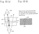
- FIGs. 11 to 12 are views for assistance in explaining the method of such position alignment.
- a concave marker 101 as shown in FIG. 11(a) is formed integrally with the substrates (the waveguide substrate 1, the lens substrate 3, the lens substrate 10, and the waveguide substrate 11) by pressing the forming glass.
- the marker 101 has a bottom surface 102 angled at 45° .
- the bottom surfaces 102 angled as described above are formed in the same direction with respect to the direction of length of the substrates.
- the horizontal positions of the markers 101 formed on the substrates are determined so that predetermined spacings are provided in the direction of length of the substrates (hereinafter, referred to as the X direction), in the direction orthogonal to the X direction within the planes of the substrates (hereinafter, referred to as the Y direction) and in the direction in which the substrates are laminated (the vertical direction, that is, the direction orthogonal to the X and the Y directions, hereinafter, referred to as the Z direction).
- the substrates are laminated so that, as shown in FIGs.
- the position of the marker 101 formed in the waveguide substrate 1 and the position of the marker 101 formed in the lens substrate 3 are the same in the Y direction of the substrates, a predetermined spacing a is provided in the X direction and a predetermined spacing c is provided in the Z direction.
- the waveguide substrate 1 is disposed below, and the lens substrate 3 is disposed above the waveguide substrate 1 through an ultraviolet cure adhesive. Then, a light source 105 emitting parallel light is disposed below the waveguide substrate 1, and a light receiver 106 such as a CCD camera is disposed above the lens substrate 3 and at a side of the laminated substrates.
- a light source 105 emitting parallel light is disposed below the waveguide substrate 1
- a light receiver 106 such as a CCD camera
- FIG. 12(b) shows images obtained from the light receiver 106 disposed above the lens substrate 3 in this manner.
- an image 108 corresponds to the marker 101 formed in the waveguide 1
- an image 107 corresponds to the marker 101 formed in the lens substrate 3.
- These images are shown on the light receiver 106 as parts darker than any peripheral part. Then, adjustment is made by moving the waveguide substrate 1 and the lens substrate 3 in the horizontal direction so that the positions of the images 107 and 108 in the Y direction coincide with each other and the spacing between the images 107 and 108 in the X direction is the predetermined spacing a.
- FIG. 12(c) shows images obtained from the light receiver 106 disposed at a side of the laminated substrates as described above.
- an image 116 corresponds to the marker 101 formed in the lens substrate 3
- an image 117 corresponds to the marker 101 formed in the waveguide substrate 1.
- These images are shown on the light receiver 106 as parts brighter than any peripheral part.
- adjustment is made by moving the waveguide 1 and the lens substrate 3 in the Z direction so that the spacing between the image 116 and the image 117 is the predetermined spacing c.
- ultraviolet light is applied to the waveguide substrate 1 and the lens substrate 3 to cure the ultraviolet-cure adhesive filling the space between the waveguide substrate 1 and the lens substrate 3, thereby bonding the substrates 1 and 3.
- position alignment is made between the lens substrate 3 and the lens substrate 10 and between the lens substrate 10 and the waveguide substrate 11.
- the position alignment between the lens substrate 3 and the lens substrate 10 is performed by an operation similar to the above-described one with the isolator substrate 8 sandwiched between the lens substrate 3 and the lens substrate 10.
- the predetermined spacing a may be different among the substrates, it is determined so that the horizontal positions of the reflecting surface 13, the lens 4, the lens 9 and the reflecting surface 9 are aligned in the vertical direction when the substrates are laminated.
- the light directed into the waveguide substrate 1 travels through the waveguide 2, and is reflected upward by the reflecting surface 13 to be incident on the lens 4.
- the light having exited from the lens 4 passes through the isolator substrate 8 and the lens 9, is horizontally reflected by the reflecting surface 4, and travels through the waveguide 12.
- the substrates are positioned so that the horizontal positions (in the X direction and in the Y direction) of the markers 101 formed in the substrates are the same in the Y direction and the predetermined spacing a is provided in the X direction, the substrates may be positioned so that a predetermined spacing b is provided in the Y direction.
- the lens substrate 10 is present between the isolator substrate 8 and the waveguide substrate 11.
- the lens substrate 10 is unnecessary. In that case, similar effects to those described above are obtained.
- the light source 105 is disposed below the waveguide substrate 1 when position alignment between the waveguide substrate 1 and the lens substrate 3 is performed, the light source 105 may be disposed at a side of the waveguide substrate 1 and the lens substrate 3 as shown in FIG. 13(a) .
- the parallel light emitted from the light source 105 is transmitted to the opposite side of the waveguide substrate 1 and the lens substrate 3 as it is to reach the light receiver 106 disposed at a side of the waveguide 1 and the lens substrate 3, and at the parts coinciding with the bottom surfaces 102 of the markers 101, part of the parallel light is reflected upward to reach the light receiver 106 disposed above the lens substrate 3.
- an image 109 corresponding to the marker 101 of the lens substrate 3 and an image 110 corresponding to the marker 101 of the waveguide substrate 1 are shown on the light receiver 106 as parts brighter than the peripheral part.
- the waveguide substrate 1 and the lens substrate 3 can be positioned in predetermined positions in the horizontal direction by adjusting the spacing a between the image 109 and the image 110 similar to the above-described case.
- FIG. 13(c) shows images obtained from the light receiver 106 disposed at a side of the waveguide substrate 1 and the lens substrate 3 as described above.
- an image 118 corresponds to the marker 101 formed in the lens substrate 3
- an image 119 corresponds to the marker 101 formed in the waveguide substrate 1.
- These images are shown on the light receiver 106 as parts darker than the peripheral part. Then, adjustment is made by moving the waveguide 1 and the lens substrate 3 in the Z direction so that the spacing between the image 118 and the image 119 is the predetermined spacing c.
- the waveguide 1 and the lens substrate 3 are bonded together similar to the above-described case.
- FIG. 11(d) shows a case where the bottom surface 104 of the convex marker 103 is angled at 45° .
- FIG. 11(e) shows a case where the bottom surface 104 of the convex marker 103 has a scattering surface.
- FIG. 11(f) shows a case where the bottom surface 104 of the convex marker 103 has a lens configuration.
- the horizontal positions and the vertical positions of the substrates can be adjusted similarly to the case of the concave markers 101 with the spacing between each substrate being fixed by a spacer (not shown) or filled with an adhesive as described above and with the light source 105 being disposed below or at a side of the waveguide 1.
- the bottom surfaces of the markers 101 and 103 are angled at 45° , they may be angled at a different angle.
- the spacing between each substrate can be similarly adjusted by observing the images shown on the light receiver 106.
- markers 101 and 103 of which bottom surfaces are inclined are used to perform the positioning of the substrates in the horizontal direction and the vertical direction, it is considered to use markers 101 having bottom surfaces 102 of a different configuration.
- FIGs. 14 (a) and 15(a) show examples of arrangement of the elements in a case where markers 101 of which bottom surfaces 102 have a lens configuration are used.
- a light source 111 is a diffusing light source, and is disposed below the waveguide substrate 1 at a predetermined distance therefrom.
- the light receiver 106 is disposed above the lens substrate 3.
- a concave marker 101 having a bottom surface 102 of a lens configuration being concave when viewed from below is disposed, and in the lens substrate 3, a concave marker 101 having a bottom surface 102 of a lens configuration being convex when viewed from below is disposed.
- the concave lens of the bottom surface 102 formed in the waveguide substrate 1 has a lens configuration and a refractive index that refract into parallel light the diffused light emitted from the light source 111 disposed at the predetermined distance from the waveguide substrate 1.
- the lens configuration as a convex lens and the refractive index of the bottom surface 102 formed in the lens substrate 103 are a lens configuration and a refractive index that condense the parallel light incident on the bottom surface 102 of the lens substrate 3 on the light receiver 106 disposed above the lens substrate 3.
- the positions of markers 101 of the substrates are the same both in the X direction and in the Y direction, or are predetermined positions. In this arrangement, when light is emitted from the light source 111, the light passes through the marker 101 of the waveguide substrate 1 and the marker 101 of the lens substrate 3 to be condensed on the light receiver 106. The images obtained from the light receiver 106 at this time are shown in FIG. 14(b) .
- an image 112 which is an image of the marker 101 itself is formed and an image 113 condensed by the bottom surface 102 having a lens configuration is formed inside the image 112.
- an image 113 condensed by the bottom surface 102 having a lens configuration is formed inside the image 112.
- the spacing between the waveguide substrate 1 and the lens substrate 3 By adjusting the spacing between the waveguide substrate 1 and the lens substrate 3 so that the outside diameter of the image 113 on the light receiver 106 is a predetermined value (that is, so that the light emitted from the light source 111 is most excellently condensed on the light receiver 106), adjustment (positioning in the vertical direction) of the spacing between the waveguide substrate 1 and the lens substrate 3 can be made. While in the FIG. 14 (b) , the two images 112 and 113 are situated side by side, these are images formed when another markers 101 of the same type are disposed so as to be situated side by side on the substrates. The markers 101 may be disposed one by one on each of the substrates as shown in Fig.14(a) .
- FIG. 15(a) shows a modification of the structure of FIG. 14 (a) .
- the bottom surface 102 of the marker 101 formed in the waveguide substrate 1 has a lens configuration being convex when viewed from below.
- the lens configurations as convex lenses and the refractive indices of the bottom surface 102 formed in the waveguide substrate 1 and the bottom surface 102 formed in the lens substrate 3 are lens configurations and refractive indices that condense the light emitted from the light source 111 on the light receiver 106 disposed above the lens substrate 3 by way of the bottom surface 102 of the waveguide substrate 1 and the bottom surface 102 of the lens substrate 3.
- images 114 and 115 are similarly formed as shown in FIG. 15(b) , and the positioning of the waveguide substrate 1 and the lens substrate 3 in the horizontal and the vertical directions can be performed similarly to the above-described case.
- FIGs. 14(a), 14(b) , 15(a) and 15(b) are described with reference to examples using the concave markers 101, the above-described applies to cases where convex markers 101 are used as shown in FIG. 11(f) .
- FIGs. 16(a) and 16(b) show a case in which the bottom surfaces 102 of the markers 101 are scattering surfaces (see FIG. 11(b) ).
- the light receiver 106 and the light source 105 are disposed below the waveguide substrate 1 so as to adjoin each other.
- the light is scattered at the scattering surfaces of the bottom surfaces 102 of the markers 101, and part of the scattered light reaches the light receiver 106 disposed below the waveguide substrate 1.
- FIG. 16(b) shows images light-received on the light receiver 106.
- an image 120 corresponds to the marker 101 formed in the lens substrate 3
- an image 121 corresponds to the marker 101 formed in the waveguide substrate 1.
- FIGs. 17(a) to 17(d) show a case where the bottom surfaces 102 of the markers 101 are inclined scattering surfaces.
- the light receiver 106 can be disposed below the waveguide substrate 1, at a side of the waveguide substrate 1 and the lens substrate 3 or above the lens substrate.
- the horizontal positions or the vertical positions of the substrates can be adjusted by applying light from the light source 105 disposed below the waveguide substrate 1.
- FIG. 17(b) shows images shown on the light receiver 106 disposed above the lens substrate 3.
- An image 122 corresponds to the marker 101 formed in the lens substrate 3
- an image 123 corresponds to the marker 101 formed in the waveguide substrate 1.
- 17(c) shows images shown on the light receiver 106 disposed at a side of the lens substrate 3 and the waveguide substrate 1.
- An image 124 corresponds to the marker 101 formed in the lens substrate 3, and an image 125 corresponds to the marker 101 formed in the waveguide substrate 1.
- FIG. 17(d) shows images shown on the light receiver 106 disposed below the waveguide substrate 1.
- An image 126 corresponds to the marker 101 formed in the lens substrate 3, and an image 127 corresponds to the marker 101 formed in the waveguide substrate 1.
- the light receiver 106 can be disposed in three directions with respect to the substrates, there is flexibility in the positioning method. For example, positioning can be performed even when the laminated substrates do not transmit light as described later. Positioning can be more precisely performed by making the adjustment while observing the light receivers 106 disposed in the three directions at the same time.
- the bottom surfaces 102 of the markers 101 are inclined lens surfaces.
- the light receiver 106 is disposed so as to be shifted from the optical axis of the light source 105.
- the bottom surfaces 102 of the markers 101 are lens surfaces having scattering surfaces.
- the markers 101 formed in the substrates are a combination of markers 101 of the same kind
- positioning may be performed with a combination of markers 101 of different kinds.
- positioning may be performed by forming in one substrate a marker 101 of which bottom surface 102 is inclined and forming in the other substrate a marker 101 of which bottom surface 102 has a scattering surface.
- positioning may be performed by forming in one substrate a marker 101 of which bottom surface 102 is inclined and forming in the other substrate a marker 101 of which bottom surface 102 has a lens surface.
- positioning may be performed by forming in one substrate a marker 101 of which bottom surface 102 has a scanning surface and forming in the other substrate a marker 101 of which bottom surface 102 has a lens surface.
- the method of positioning of the substrates is described as a case where positioning of the waveguide substrate 1 and the lens substrate 3 is performed, it is similarly applicable to a case where positioning of other substrates (that is, the planar substrates of the present invention) is performed.
- positioning is performed by applying light from below the substrates, it is considered to apply light from above the substrates.
- the waveguide substrate 12 is further laminated on the lens substrate 10 and positioning of the lens substrate 10 and the waveguide substrate 11 is performed, the light source 105 and the light receiver 106 are disposed above the waveguide substrate 11 and the light receiver 106 is disposed at a side of the lens substrate 10 and the waveguide substrate 11.
- markers 101 of which bottom surfaces 102 are inclined scattering surfaces are used.
- a waveguide substrate 31 has two waveguides 22 and 32.
- the waveguide 32 is disposed on the farther side from the plane of FIG. 3 so as to be parallel to the waveguide 22.
- the waveguide 22 has a reflecting surface 313 at its end, and the waveguide 32 has a reflecting surface 333 at its end.
- the lens substrate 33 has a lens 34 corresponding to the reflecting surface 313 and a lens 304 corresponding to the reflecting surface 333.
- a lens substrate 30 having a lens 29 corresponding to the lens 34 is laminated, and above the lens substrate 30, a waveguide substrate 31 is laminated having a waveguide 312 and a reflecting surface 314 disposed at an end of the waveguide 312 and corresponding to the lens 29.
- a lens substrate 300 having a lens 209 corresponding to the lens 304 is laminated, and above a lens substrate 300, a waveguide substrate 301 is laminated having a waveguide 302 and a reflecting surface 324 disposed at an end of the waveguide 302 and corresponding to the lens 209.
- the reflecting surfaces 313 and 333 are angled at 45° like the reflecting surface 13 in the first embodiment, and the reflecting surfaces 314 and 324 are angled 45° like the reflecting surface 14 in the first embodiment.
- the horizontal positions of the reflecting surface 313, the lens 34, the lens 29 and the reflecting surface 314 are aligned in the vertical direction, and the horizontal positions of the reflecting surface 333, the lens 304, the lens 209 and the reflecting surface 324 are aligned in the vertical direction.
- positioning of the waveguide substrate 31 and the lens substrate 33, positioning of the lens substrate 33 and the lens substrate 30, positioning of the lens substrate 30 and the waveguide substrate 31, positioning of the waveguide substrate 31 and the lens substrate 300 and positioning of the lens substrate 300 and the waveguide substrate 301 are performed similarly to the first embodiment (the same applied to the embodiments described below).
- the lights directed into the waveguides 22 and 32 of the waveguide substrate 31 are directed to the waveguides 312 and 302, respectively, by an action similar to that of the first embodiment.
- the planar substrates of the present invention by laminating the planar substrates of the present invention and three-dimensionally forming two waveguides, a low-cost and high-performance three-dimensional optical waveguide not requiring a complicated adjustment is provided.
- the lens substrate 30 is present between the isolator substrate 8 and the waveguide substrate 31 and the lens substrate 300 is present between the waveguide substrate 31 and the waveguide substrate 301, when it is possible that the light reflected by the reflecting surface 313 is condensed on the reflecting surface 314 only by the lens 44 and the light reflected by the reflecting surface 333 is condensed on the reflecting surface 324 only by the lens 404 as shown in FIG. 4 , the lens substrates 30 and 300 are unnecessary. In that case, similar effects to those described above are obtained.
- the waveguide 32 is disposed on the farther side from the plane of FIG. 3 so as to be parallel to the waveguide 22, the arrangement of the waveguides 22 and 32 is not limited thereto. Similar effects to those described above are obtained from any arrangement as long as the waveguides 22 and 32 are separately disposed on the same waveguide substrate 31 and the lights directed thereinto are directed to the other waveguides 312 and 302, respectively.
- the waveguides 22 and 32 are not necessarily present on the same waveguide substrate 31 but may be present on different laminated waveguide substrates, and the waveguides 312 and 302 are not necessarily present on the waveguide substrates 31 and 301 but may be present on the same waveguide substrate. In these cases, similar effects to those described above are obtained.
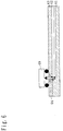
- FIG. 5 shows the structure of a three-dimensional optical waveguide according to a third embodiment of the present invention.
- a surface emitting laser (VCSEL) 59 which is the light emitting element of the present invention is disposed above the isolator substrate 8, and a reflecting surface 513, a lens 54 and the surface emitting laser 59 are disposed so that the horizontal positions thereof are aligned in the vertical direction.
- VCSEL surface emitting laser
- the structure of the part constituted by a waveguide substrate 51, a lens substrate 53 and the isolator substrate 8 is similar to that of the first embodiment, and description thereof is omitted.
- the laser beam emitted from the surface emitting laser 59 passes through the isolator substrate 8 and the lens 54 to be directed to the waveguide 52 of the waveguide substrate 51.
- the isolator substrate 8 is present between the lens substrate 53 and the surface emitting laser 59, the isolator substrate 8 is not necessarily present. In that case, similar effects to those described above are obtained.
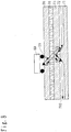
- FIG. 6 shows a three-dimensional optical waveguide comprising a waveguide substrate 61 having a waveguide 62, a lens substrate 63 having a lens 64 and the surface-mount photodiode 69.
- the structure of the waveguide substrate 61 and the lens substrate 63 is similar to the above-described structure, and description thereof is omitted.
- the isolator substrate 8 may be laminated between the lens substrate 63 and the surface-mount photodiode 69.
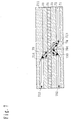
- FIG. 7 shows the structure of a three-dimensional optical waveguide according to a fourth embodiment of the present invention.
- a waveguide substrate 71 has a waveguide 72, and a waveguide 702 in a direction opposed to the waveguide 72.
- a reflecting surface 713 is formed, and at an end of the waveguide 702, a reflecting surface 733 is formed.
- the reflecting surfaces 713 and 733 are formed so as to be opposed to each other and each angled at approximately 22.5° from the horizontal plane in a direction that forms a slope of a trapezoidal shape.
- a lens 74 and a lens 704 are formed integrally with the lens substrate 73 so as to adjoin each other.
- a wavelength division multiplexing filter 76 which is the planar substrate having a filter layer of the present invention is laminated, and above the wavelength division multiplexing filter 76, a lens substrate 70 having a lens 79 is laminated.
- a waveguide substrate 711 is laminated having a waveguide 712 and a reflecting surface 714 formed at an end of the waveguide 712.
- the reflecting surface 714 is angled at approximately 22.5° from the horizontal plane.
- the lens 74, the lens 79 and the reflecting surface 714 are aligned so as to be inclined toward the upper left by 45° from the horizontal plane.
- the lens 704 is inclined by 45° from the horizontal direction in a direction slanting upward toward the right.
- the light traveling leftward in the horizontal direction through the waveguide 72 is reflected upward by the reflecting surface 713 at 45° from the horizontal travel direction, and passes through the lens 74.
- Part of the light having passed through the lens 74 passes through the wavelength division multiplexing filter 76 (that is, is sorted out by the wavelength division multiplexing filter), reaches the reflecting surface 714 through the lens 79 to be reflected in the horizontal direction, and travels leftward through the waveguide 712.
- the light including the remaining wavelength component sorted out by the wavelength division multiplexing filter 76 is reflected at 45° from the horizontal direction in a direction slanting downward toward the left at the interface between the lens substrate 73 and the wavelength division multiplexing filter 76, is reflected by the reflecting surface 733 through the lens 704, and travels leftward in the horizontal direction through the waveguide 702.
- the light incident on the waveguide 72 can be extracted after being separated between light traveling through the waveguide 712 and light traveling through the waveguide 702 according to the wavelength component.
- the lens substrate 70 when it is possible that light is sufficiently condensed on the reflecting surface 714 by the lens 74, the lens substrate 70 is unnecessary. In that case, similar effects to those described above are obtained.
- FIG. 8 shows a modification of the present embodiment.
- a surface-mount photodiode 89 is disposed instead of laminating the waveguide substrate 711.
- positioning of the substrates is performed by applying light from above the three-dimensional optical waveguide as required.
- positioning of the waveguide substrate 711 is performed under a condition where the waveguide substrate 71, the lens substrate 73, the wavelength division multiplexing filter 76 and the lens substrate 70 are laminated as shown in FIG. 7
- the wavelength of the light emitted from the light source 105 does not pass through the wavelength division multiplexing filter 76
- the light source 105 is disposed above the waveguide substrate 711, and positioning of the waveguide substrate 711 is performed by applying light from above by a method similar to that described in the first embodiment.
- FIG. 9 shows the structure of a three-dimensional optical waveguide of the present invention according to a fifth embodiment.
- the three-dimensional optical waveguide of the present embodiment has on the left side thereof a three-dimensional optical waveguide where a lens substrate 900 having a lens 919 is laminated above the three-dimensional optical waveguide shown in the third embodiment ( FIG. 5 ), and has on the right side thereof the three-dimensional optical waveguide shown in the fourth embodiment ( FIG. 8 ) .
- the thickness of the lens substrate 900 is different between the left side and the right side thereof.
- the thickness of the right side of the three-dimensional optical waveguide of the present embodiment is larger than that of the left side by the thickness of a Faraday rotator 96 and the thickness of a polarizer 97.
- a wavelength division multiplexing filter 906 is designed so as to reflect the wavelength of the light emitted from a surface emitting laser 99 and transmit the wavelength of the light incident from a waveguide 92.
- the elements other than these are similar to those of the third and the fourth embodiments, and description thereof is omitted.
- the light traveling leftward through the waveguide 92 is reflected upward by a reflecting surface 913 at 45° from the horizontal travel direction, passes through a lens 94, the wavelength division multiplexing filter 906 and a lens 909, and reaches a surface-mount photodiode 999.
- the light emitted from the surface emitting laser 99 passes downward through the lens 919, an isolator substrate 98 and a lens 914, is reflected rightward in the horizontal direction by a reflecting surface 943, and is then reflected upward by a reflecting surface 933 in a direction 45° from the direction of travel.
- the light reflected by the reflecting surface 933 passes through a lens 904, is reflected at 45° in a direction slanting downward toward the right at the interface between the wavelength division multiplexing filter 906 and a lens substrate 93, passes through the lens 94, and reaches the reflecting surface 913.
- the light reflected rightward in the horizontal direction by the reflecting surface 913 travels rightward through the waveguide 92.
- a low-cost and high-performance three-dimensional optical waveguide is provided that does not require a complicated adjustment although having a complicated structure.
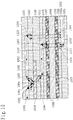
- FIG. 10 shows the structure according to a sixth embodiment of the present invention.
- the structure of the right side of the three-dimensional optical waveguide shown in FIG. 10 is similar to the structure of the three-dimensional optical waveguide shown in the second embodiment ( FIG. 3 ), and description thereof is omitted.
- the structure of the left side of the three-dimensional optical waveguide shown in FIG. 10 is one obtained by vertically and horizontally reversing the structure of the three-dimensional optical waveguide shown in the fourth embodiment ( FIG. 7 ).
- a wavelength division multiplexing filter 1316 which is an example of the wavelength division multiplexing filter of the present invention is set so as to transmit light of a wavelength ⁇ 1 and not to transmit light of a wavelength ⁇ 2.
- the light of the wavelength A 1 directed into the waveguide 1322 reaches a reflecting surface 1373 through a reflecting surface 1313, a lens 1334, an isolator substrate 1308, a lens 1324, a reflecting surface 1363 and a waveguide 1342.
- the light reflected by the reflecting surface 1373 passes through a lens 1344, the wavelength division multiplexing filter 1316 and a lens 1364, is reflected by a reflecting surface 1393, and reaches a waveguide 1362.
- the light of the wavelength ⁇ 2 directed into the waveguide 1332 reaches a reflecting surface 1383 through a reflecting surface 1333, a lens 1304, the isolator substrate 1308, a lens 1314 and a reflecting surface 1353.
- the light reflected by the reflecting surface 1383 is incident, through a lens 1354, on the wavelength division multiplexing filter 1316 from the upper right in a slanting direction.
- the wavelength division multiplexing filter 1316 does not transmit light of the wavelength ⁇ 2
- the light incident from the upper right of the wavelength division multiplexing filter 1316 in a slanting direction is reflected at the interface between the wavelength division multiplexing filter 1316 and a lens substrate 1350, travels in a direction slanting upward toward the left, and is directed into a waveguide 1362 through the lens 1364 and the reflecting surface 1393.
- FIG. 19 is an example of the structure of such an optical transmitter module.
- a laser diode 1109 which is an example of the light emitting element of the present invention is connected.
- the laser diode 1109 is connected to a waveguide 1102.
- the waveguide 1102 is connected to a waveguide 1112 through an isolator 1108.
- an optical output terminal 1107 is connected to the waveguide 1112.
- Such an optical transmitter module can be formed, for example, by using the three-dimensional optical waveguide shown in FIG. 1 which is an example of the three-dimensional optical waveguide of the present invention.
- the waveguide 1102 in FIG. 19 corresponds to the waveguide 2 shown in FIG. 1 , and to an end thereof, the laser diode 1109 (in this case, an edge emitting laser) is attached.
- the waveguide 1112 in FIG. 19 corresponds to the waveguide 12 shown in FIG. 1 , and at an end thereof, for example, a V groove 1042 shown in FIG. 25 is disposed as the optical output terminal 1107, and an optical fiber cable (not shown) is fixed.
- an optical output can be output from the output terminal 1107 in accordance with the electric signal input to the electric input terminal 1105, so that a low-cost optical transmitter module not requiring a complicated adjustment is provided.
- the three-dimensional optical waveguide shown in FIG. 2 may be used.
- the three-dimensional optical waveguide as shown in FIG. 3 or FIG. 4 may be used.
- the two waveguides 22 and 32 correspond to the waveguide 1102
- the two waveguides 312 and 302 correspond to the waveguide 1112.
- the laser diode 1109 is disposed, and to an end of each of the waveguides 312 and 302, the optical output terminal 1107 is connected.
- the light emitted from each laser diode 1109 is output from the optical output terminal 1107.
- the three-dimensional optical waveguide shown in FIG. 5 may be used. In that case, the waveguide 1102 is omitted, and as the laser diode 1109, the surface emitting laser 59 is used.
- FIG. 20 shows an example of the structure of a wavelength division multiplexing optical transmitter module.
- the wavelength division multiplexing optical transmitter module shown in FIG. 20 has two laser diodes 1119 and 1129 each having the electric input terminal 1105. To the laser diodes 1119 and 1129, the waveguides 1132 and 1142 are connected, respectively. The waveguides 1132 and 1142 are connected to waveguides 1152 and 1162 through an isolator 1118, respectively. The waveguides 1152 and 1162 are connected to the optical output terminal 1107 through the wavelength division multiplexing filter 1106.
- Such a wavelength division multiplexing optical transmitter module can be formed, for example, by using the three-dimensional optical waveguide of the structure shown in FIG. 10 .
- the laser diode 1119 outputting light of the wavelength ⁇ 1 is disposed at an end of the waveguide 1322
- the laser diode 1129 outputting light of the wavelength ⁇ 2 is disposed at an end of the waveguide 1332.
- the output terminal 1107 is disposed at an end of the waveguide 1362.
- the electric signals input from the two laser diodes 1119 and 1129 can be output as combined with each other as an optical signal.
- FIG. 21 shows an example of the structure of an optical receiver module.
- an optical input terminal 1117 for example, the V groove shown in FIG. 25
- a photodiode 1209 which is an example of the light receiving element of the present invention is connected to the waveguide 1122.
- an electric output terminal 1115 is connected to the photodiode 1209.
- Such an optical receiver module can be structured, for example, by using the three-dimensional optical waveguide shown in FIG. 6 which is an example of the three-dimensional optical waveguide. According to the optical receiver module having such a structure, electric output can be obtained from' the electric output terminal 1115 in accordance with the optical signal input to the optical input terminal 1117.
- FIG. 22 shows an example of the structure of a wavelength division multiplexing optical receiver module.
- the optical input terminal 1117 is connected to the wavelength division multiplexing filter 1116
- waveguides 1172 and 1182 are connected to the wavelength division multiplexing filter 1116
- photodiodes 1219 and 1229 are connected to the waveguides 1172 and 118, respectively.
- Such a wavelength division multiplexing optical receiver module can be structured, for example, by using the three-dimensional optical waveguide shown in FIG. 7 .
- the optical input terminal 1117 is connected to an end of the waveguide 72, and the photodiodes 1219 and 1229 are connected to ends of the waveguides 712 and 702, respectively.
- the wavelength division multiplexing filter 76 is set so as to transmit light of the wavelength ⁇ 1 and not to transmit light of the wavelength ⁇ 2.
- the wavelength division multiplexing optical receiver module having such a structure, when lights of the wavelength A 1 and the wavelength ⁇ 2 are directed into the waveguide 71, the light of the wavelength ⁇ 1 reaches the photodiode 1219 through the waveguide 712, the light of the wavelength ⁇ 2 reaches the photodiode 1229 through the waveguide 702, and in accordance therewith, electric output is output from the electric output terminal 1115 connected to each of the photodiodes 1219 and 1229. That is, an optical signal input from one optical input terminal 1117 can be obtained from each electric output terminal 1115 as two separate electric signals.
- optical transmitter module and optical receiver module can be used as an optical transmission system for transmission and reception by being connected through an optical fiber cable.
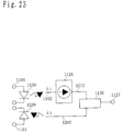
- FIG. 23 shows an example of the structure of a wavelength division multiplexing optical transmitter and receiver module having both an optical transmission function and an optical reception function.
- a laser diode 1139 having the electric input terminal 1105 and emitting light of the wavelength ⁇ 1 is connected to a wavelength division multiplexing filter 1126 which is an example of the wavelength division multiplexing filter of the present invention through a waveguide 1192, an isolator 1128 which is an example of the isolator of the present invention and a waveguide 1212.
- the photodiode 1239 having the electric output terminal 1115 and receiving light of the wavelength ⁇ 2 is connected to the wavelength division multiplexing filter 1126 through a waveguide 1202.
- an optical input and output terminal 1127 (for example, the V groove shown in FIG. 25 ) which is an example of the optical input and output terminal of the present invention is connected.
- Such a wavelength division multiplexing optical transmitter and receiver module can be structured, for example, by using the three-dimensional optical waveguide shown in FIG. 9 .
- the optical input and output terminal 1127 is disposed at an end of the waveguide 92.
- the wavelength division multiplexing filter 906 is set so as not to transmit light of the wavelength ⁇ 1 emitted from the surface emitting laser 99 and to transmit light of the wavelength ⁇ 2 input to the optical input and output terminal 1127.
- the light of the wavelength ⁇ 1 emitted from the surface emitting laser 99 is reflected at the interface between the wavelength division multiplexing filter 906 and the lens substrate 93, and is output from the optical input and output terminal 1127 through the waveguide 92.
- the light of the wavelength ⁇ 2 input to the optical input and output terminal 1127 passes through the wavelength division multiplexing filter 906 to reach the surface-mount photodiode 999.
- light can be transmitted and received with only one optical input and output terminal 1127.
- FIG. 24 shows an example of a light transmission apparatus using such a wavelength division multiplexing optical transmitter and receiver module.
- a laser diode driver IC 1104 is connected to the laser diode 1149, and to the laser diode driver IC 1104, a transmission signal multiplexer 1103 is connected.
- an electric signal input terminal 1125 for inputting a plurality of signals is connected to the transmission signal multiplexer 1103, an electric signal input terminal 1125 for inputting a plurality of signals is connected.
- the laser diode driver IC 1104 controls the current bias supplied to the laser diode, and superimposes digital signals.
- a reception front end IC 1114 is connected to a photodiode 1249, and to the reception front end IC 1114, a reception signal demultiplexer 1113 is connected. To the reception signal demultiplexer 1113, a reception signal output terminal 1135 for outputting a plurality of signals is connected.
- the reception front end IC 1114 low-noise-amplifies the faint signal output from the photodiode 1249.
- the laser diode 1149 and the elements disposed on the right side of the photodiode 1249 are as described above.
- a plurality of electric signals can be transmitted on an optical fiber cable through one optical input and output terminal.
- a plurality of the above-described optical modules for transmission and reception can be used as an optical transmission system for transmission and reception by being connected through an optical fiber cable.
- two optical modules for transmission and reception prepared as a pair can be used as a pair of optical transmission systems for transmission and reception by making a setting such that one optical transmitter and receiver module performs transmission at the wavelength ⁇ 1 and reception at the wavelength ⁇ 2 and the other optical transmitter and receiver module performs transmission at the wavelength ⁇ 2 and reception at the wavelength ⁇ 1.
- light from a horizontal direction is made to travel in the vertical direction or at an angle of 45°
- the light may be made to travel at an arbitrary angle with respect to the laminated substrates.
- the angles of the reflecting surfaces and the arrangement of the lenses and the reflecting surfaces are settable so that the light travels in such a manner.
- the substrates are formed of forming glass, they may be formed of resin or the like.
- the substrates may be formed, for example, by forming the markers 101 and 103 at the same time together with the waveguides on a silicon substrate by dry etching. In that case, similar effects to those described above are obtained.
- the planar substrates other than the one having a waveguide may be sheet optical elements in addition to or instead of the lens layer, the isolator layer and the filter layer.
- sheet optical elements include a sheet attenuator attenuating optical power.
- a low-cost three-dimensional optical waveguide not requiring a complicated adjustment can be provided.
- planar waveguide, and the lens layer, the isolator layer or the filter layer are integrally formed on forming glass, a low-cost three-dimensional optical waveguide further not requiring a complicated adjustment can be provided.
- planar substrate has the lens layer, the isolator layer or the filter layer, a high-performance three-dimensional optical waveguide can be provided.
- a precise and low-cost three-dimensional optical waveguide not requiring a complicated adjustment can be provided.
- optical module having the three-dimensional optical waveguide of the present invention a low-cost optical module not requiring a complicated adjustment can be provided.
Claims (5)
- Guide d'onde optique en trois dimensions, comprenant une stratification d'au moins:un premier substrat plan (1, 61, 71) ayant un guide d'onde optique plan (2, 62, 72), le guide d'onde optique plan étant sur la surface supérieure du premier substrat plan; etun second substrat plan (3, 63, 73) ayant une couche de lentille de verre de formage, et éventuellement une couche isolante (8) ou une couche filtrante (76), dans lequel une lentille (4, 64, 74) est formée d'une seule pièce de verre de formage dans la couche de lentille,dans lequel le guide d'onde optique plan (2, 62, 72) comprend une surface réfléchissante (13, 713) configurée de telle sorte que la lumière traverse la couche de lentille (3, 63, 73), et, le cas échéant, la couche d'isolation (8) et la couche filtrante (76);caractérisé en ce quele premier substrat plan (1, 61, 71) est constitué de verre de formage, età la fois le premier substrat plan (1, 61, 71) et le second substrat plan (3, 63, 73) comprennent des marqueurs (101, 103) de verre de formage présentant une forme convexe ou concave et ayant la propriété d'être transparents à la lumière.
- Guide d'onde optique en trois dimensions selon la revendication 1, comprenant en outre au moins l'un d'un élément de réception de lumière (69, 89, 999) et d'un élément d'émission de lumière (59, 99).
- Guide d'onde optique en trois dimensions selon la revendication 1, dans lequel le premier substrat plan et le second substrat plan sont positionnés l'un par rapport à l'autre par les marqueurs (101, 103) formées sur les surfaces de jonction à la fois du premier substrat plan et du second substrat plan.
- Module émetteur et récepteur optique comprenant:une borne d'entrée électrique (1105);un guide d'onde optique en trois dimensions selon la revendication 1;un élément d'émission de lumière (1139) connecté à la borne d'entrée électrique (1105) et connecté au guide d'onde optique en trois dimensions;un élément de réception de lumière (1239) connecté au guide d'onde optique en trois dimensions;une borne de sortie électrique (1115) connectée à l'élément de réception de lumière (1239);
etune borne d'entrée et de sortie optique (1127) connectée au guide d'onde optique en trois dimensions,dans lequel une entrée de signal électrique provenant de la borne d'entrée électrique (1105) est convertie en un signal optique et transmise à partir de la borne d'entrée et de sortie optique,et un signal optique reçu par la borne d'entrée et de sortie optique (1127) est converti en un signal électrique et délivré en sortie à la borne de sortie électrique (1115). - Système de transmission optique pour transmission et réception optique comprenant:le module émetteur et récepteur optique selon la revendication 4; etun câble à fibre optique connecté au module d'émetteur et récepteur optique.
Applications Claiming Priority (2)
| Application Number | Priority Date | Filing Date | Title |
|---|---|---|---|
| JP2002054375A JP3768901B2 (ja) | 2002-02-28 | 2002-02-28 | 立体光導波路の製造方法 |
| JP2002054375 | 2002-02-28 |
Publications (3)
| Publication Number | Publication Date |
|---|---|
| EP1341019A2 EP1341019A2 (fr) | 2003-09-03 |
| EP1341019A3 EP1341019A3 (fr) | 2004-09-29 |
| EP1341019B1 true EP1341019B1 (fr) | 2017-12-13 |
Family
ID=27678567
Family Applications (1)
| Application Number | Title | Priority Date | Filing Date |
|---|---|---|---|
| EP03004550.4A Expired - Fee Related EP1341019B1 (fr) | 2002-02-28 | 2003-02-28 | Guide d'onde optique en trois dimensions |
Country Status (4)
| Country | Link |
|---|---|
| US (3) | US20030161573A1 (fr) |
| EP (1) | EP1341019B1 (fr) |
| JP (1) | JP3768901B2 (fr) |
| CN (1) | CN1328604C (fr) |
Families Citing this family (70)
| Publication number | Priority date | Publication date | Assignee | Title |
|---|---|---|---|---|
| US7343058B2 (en) * | 2003-04-22 | 2008-03-11 | Intel Corporation | Efficient light coupler from off-chip to on-chip waveguides |
| CN100495094C (zh) * | 2003-04-23 | 2009-06-03 | 斯欧普迪克尔股份有限公司 | 在soi光学平台上形成的亚微米平面光波设备 |
| US7251393B2 (en) * | 2004-03-30 | 2007-07-31 | Lockheed Martin Corporation | Optical router |
| US7389013B2 (en) * | 2004-09-30 | 2008-06-17 | Stmicroelectronics, Inc. | Method and system for vertical optical coupling on semiconductor substrate |
| US7391937B2 (en) * | 2004-10-22 | 2008-06-24 | Lockheed Martin Corporation | Compact transition in layered optical fiber |
| JP4587772B2 (ja) * | 2004-10-22 | 2010-11-24 | イビデン株式会社 | 多層プリント配線板 |
| JP5005168B2 (ja) * | 2004-12-06 | 2012-08-22 | ソニー株式会社 | 光導波装置及びその製造方法、並びに光情報処理装置及び電子機器 |
| US7298941B2 (en) * | 2005-02-16 | 2007-11-20 | Applied Materials, Inc. | Optical coupling to IC chip |
| US7189584B2 (en) * | 2005-04-27 | 2007-03-13 | Hewlett-Packard Development Company, L.P. | Fabrication alignment technique for light guide screen |
| JP2008040003A (ja) | 2006-08-03 | 2008-02-21 | Fuji Xerox Co Ltd | フレキシブル光導波路フィルム、光送受信モジュール、マルチチャンネル光送受信モジュール及びフレキシブル光導波路フィルムの製造方法 |
| US8867868B2 (en) * | 2006-10-03 | 2014-10-21 | Kabushiki Kaisha Toshiba | Semiconductor integrated circuit |
| WO2008062836A1 (fr) * | 2006-11-22 | 2008-05-29 | Nikon Corporation | Module de guide d'onde optique et son procédé de fabrication |
| US7646949B2 (en) * | 2007-07-27 | 2010-01-12 | Kotura, Inc. | Efficient transfer of light signals between optical devices |
| WO2010123595A2 (fr) * | 2009-01-15 | 2010-10-28 | Mayo Foundation For Medical Education And Research | Connecteur optique latéral |
| CN101872043B (zh) * | 2010-06-12 | 2013-09-04 | 中央大学 | 光学传输模块 |
| JP2012063969A (ja) * | 2010-09-16 | 2012-03-29 | Nitto Denko Corp | 光導波路デバイスおよび光学式タッチパネル |
| KR20120048258A (ko) * | 2010-11-05 | 2012-05-15 | 한국전자통신연구원 | 경사진 거울 및 렌즈를 구비한 광 도파로 구조체 |
| US9164247B2 (en) * | 2011-07-28 | 2015-10-20 | Source Photonics, Inc. | Apparatuses for reducing the sensitivity of an optical signal to polarization and methods of making and using the same |
| EP2761345B1 (fr) * | 2011-09-26 | 2017-11-08 | 3M Innovative Properties Company | Substrat optique comprenant plusieurs éléments de redirection de la lumière en quinconce sur une surface principale de celui-ci |
| TWI511477B (zh) * | 2011-12-07 | 2015-12-01 | Hon Hai Prec Ind Co Ltd | 光收發裝置 |
| US20130188970A1 (en) * | 2012-01-19 | 2013-07-25 | Kalpendu Shastri | Packaging Platform For Opto-Electronic Assemblies Using Silicon-Based Turning Mirrors |
| JP5877749B2 (ja) * | 2012-03-29 | 2016-03-08 | 日東電工株式会社 | 光電気混載基板の製法 |
| JP6246191B2 (ja) * | 2012-05-29 | 2017-12-13 | スリーエム イノベイティブ プロパティズ カンパニー | 光配線 |
| KR102009979B1 (ko) * | 2012-06-07 | 2019-08-12 | 삼성전자주식회사 | 반도체 패키지 및 이를 포함하는 반도체 장치 |
| JP6081086B2 (ja) | 2012-06-14 | 2017-02-15 | Tdk株式会社 | 光電素子用実装装置及び実装方法 |
| ITTO20120583A1 (it) * | 2012-07-02 | 2014-01-03 | St Microelectronics Srl | Dispositivo optoelettronico integrato con guida d'onda e relativo procedimento di fabbricazione |
| KR20140064530A (ko) * | 2012-11-20 | 2014-05-28 | 삼성전자주식회사 | 광 연결을 포함하는 다중 칩 패키지 |
| US9052464B1 (en) * | 2013-01-18 | 2015-06-09 | Kotura, Inc. | Transfer of light signals between optical devices |
| US9094135B2 (en) * | 2013-06-10 | 2015-07-28 | Freescale Semiconductor, Inc. | Die stack with optical TSVs |
| US9435952B2 (en) | 2013-06-10 | 2016-09-06 | Freescale Semiconductor, Inc. | Integration of a MEMS beam with optical waveguide and deflection in two dimensions |
| US9766409B2 (en) | 2013-06-10 | 2017-09-19 | Nxp Usa, Inc. | Optical redundancy |
| US10230458B2 (en) | 2013-06-10 | 2019-03-12 | Nxp Usa, Inc. | Optical die test interface with separate voltages for adjacent electrodes |
| US9442254B2 (en) | 2013-06-10 | 2016-09-13 | Freescale Semiconductor, Inc. | Method and apparatus for beam control with optical MEMS beam waveguide |
| US9810843B2 (en) | 2013-06-10 | 2017-11-07 | Nxp Usa, Inc. | Optical backplane mirror |
| US9086551B2 (en) * | 2013-10-30 | 2015-07-21 | International Business Machines Corporation | Double mirror structure for wavelength division multiplexing with polymer waveguides |
| CA3168318A1 (fr) * | 2014-09-29 | 2016-04-07 | Magic Leap, Inc. | Architectures et procedes pour delivrer de la lumiere a des longueurs d'onde differentes d'un guide d'ondes |
| NZ773847A (en) | 2015-03-16 | 2022-07-01 | Magic Leap Inc | Methods and systems for diagnosing and treating health ailments |
| CN107924085B (zh) | 2015-06-15 | 2022-09-02 | 奇跃公司 | 虚拟和增强现实系统以及方法 |
| US10992104B2 (en) | 2015-12-17 | 2021-04-27 | Ii-Vi Delaware, Inc. | Dual layer grating coupler |
| CN108701962B (zh) | 2015-12-17 | 2021-04-16 | 菲尼萨公司 | 表面耦合系统 |
| US10739518B2 (en) * | 2015-12-21 | 2020-08-11 | International Business Machines Corporation | Optical components for wavelength division multiplexing with high-density optical interconnect modules |
| US9791640B2 (en) * | 2016-03-14 | 2017-10-17 | Te Connectivity Corporation | Interposer with separable interface |
| NZ747005A (en) | 2016-04-08 | 2020-04-24 | Magic Leap Inc | Augmented reality systems and methods with variable focus lens elements |
| CN113219579A (zh) | 2016-05-12 | 2021-08-06 | 奇跃公司 | 成像波导上的分布式光操纵 |
| CN106159565A (zh) * | 2016-08-22 | 2016-11-23 | 安费诺电子装配(厦门)有限公司 | 一种带拉带脱锁结构的高速连接器模组及组装方法 |
| KR102639600B1 (ko) | 2016-11-18 | 2024-02-21 | 매직 립, 인코포레이티드 | 넓은 입사 각도 범위들의 광을 방향전환시키기 위한 다중층 액정 회절 격자들 |
| WO2018094093A1 (fr) | 2016-11-18 | 2018-05-24 | Magic Leap, Inc. | Multiplexeur de lumière à guide d'ondes utilisant des réseaux croisés |
| IL303676B1 (en) | 2016-11-18 | 2024-02-01 | Magic Leap Inc | Liquid crystal refraction lattices vary spatially |
| US11067860B2 (en) | 2016-11-18 | 2021-07-20 | Magic Leap, Inc. | Liquid crystal diffractive devices with nano-scale pattern and methods of manufacturing the same |
| CA3045663A1 (fr) | 2016-12-08 | 2018-06-14 | Magic Leap, Inc. | Dispositifs de diffraction bases sur du cristal liquide cholesterique |
| KR102550742B1 (ko) | 2016-12-14 | 2023-06-30 | 매직 립, 인코포레이티드 | 표면 정렬 패턴들의 소프트-임프린트 복제를 이용한 액정들의 패터닝 |
| US10371896B2 (en) | 2016-12-22 | 2019-08-06 | Magic Leap, Inc. | Color separation in planar waveguides using dichroic filters |
| AU2018210527B2 (en) | 2017-01-23 | 2022-12-01 | Magic Leap, Inc. | Eyepiece for virtual, augmented, or mixed reality systems |
| US10359565B2 (en) | 2017-02-07 | 2019-07-23 | Nokia Of America Corporation | Optoelectronic circuit having one or more double-sided substrates |
| JP7158395B2 (ja) | 2017-02-23 | 2022-10-21 | マジック リープ, インコーポレイテッド | 偏光変換に基づく可変焦点画像デバイス |
| IL303471A (en) | 2017-03-21 | 2023-08-01 | Magic Leap Inc | An eye imaging device that uses optical refractive elements |
| JP6842377B2 (ja) * | 2017-06-20 | 2021-03-17 | 日本電信電話株式会社 | 平面光回路積層デバイス |
| KR20190009515A (ko) * | 2017-07-19 | 2019-01-29 | 삼성전자주식회사 | 반도체 장치 |
| JP7280250B2 (ja) | 2017-09-21 | 2023-05-23 | マジック リープ, インコーポレイテッド | 眼および/または環境の画像を捕捉するように構成される導波管を伴う拡張現実ディスプレイ |
| CN111683584A (zh) | 2017-12-15 | 2020-09-18 | 奇跃公司 | 用于增强现实显示系统的目镜 |
| US10705302B2 (en) * | 2018-02-27 | 2020-07-07 | Samsung Electronics Co., Ltd. | Photonic integrated circuit packages |
| US11435522B2 (en) | 2018-09-12 | 2022-09-06 | Ii-Vi Delaware, Inc. | Grating coupled laser for Si photonics |
| WO2020106824A1 (fr) | 2018-11-20 | 2020-05-28 | Magic Leap, Inc. | Oculaires destinés à un système d'affichage à réalité augmentée |
| EP3899620A1 (fr) * | 2018-12-18 | 2021-10-27 | Telefonaktiebolaget LM Ericsson (publ) | Interconnexion optique et procédé de fabrication associé |
| US11404850B2 (en) | 2019-04-22 | 2022-08-02 | Ii-Vi Delaware, Inc. | Dual grating-coupled lasers |
| US11650423B2 (en) | 2019-06-20 | 2023-05-16 | Magic Leap, Inc. | Eyepieces for augmented reality display system |
| CN111146682B (zh) * | 2019-12-04 | 2021-02-26 | 上海传输线研究所(中国电子科技集团公司第二十三研究所) | 一种光纤耦合半导体激光器模块及半导体激光器 |
| WO2023026572A1 (fr) * | 2021-08-26 | 2023-03-02 | 株式会社村田製作所 | Composant optique |
| WO2023105591A1 (fr) * | 2021-12-06 | 2023-06-15 | 日本電信電話株式会社 | Circuit optique |
| US11650381B1 (en) | 2022-02-12 | 2023-05-16 | Globalfoundries U.S. Inc. | PIC die and package with cover for multiple level and multiple depth connections of fibers to on-chip optical components |
Citations (2)
| Publication number | Priority date | Publication date | Assignee | Title |
|---|---|---|---|---|
| GB2301681A (en) * | 1995-05-27 | 1996-12-11 | Bosch Gmbh Robert | Connecting integrated optical components using inclined reflecting surfaces |
| DE10054370A1 (de) * | 2000-10-30 | 2002-05-16 | Infineon Technologies Ag | Optisches Verteilerelement |
Family Cites Families (35)
| Publication number | Priority date | Publication date | Assignee | Title |
|---|---|---|---|---|
| DE3834335A1 (de) * | 1988-10-08 | 1990-04-12 | Telefunken Systemtechnik | Halbleiterschaltung |
| US5198008A (en) * | 1990-11-09 | 1993-03-30 | National Semiconductor Corporation | Method of fabricating an optical interconnect structure |
| US5416861A (en) * | 1994-04-29 | 1995-05-16 | University Of Cincinnati | Optical synchronous clock distribution network and high-speed signal distribution network |
| US5911022A (en) * | 1994-09-29 | 1999-06-08 | Siemens Aktiengesellschaft | Optical coupling arrangement |
| GB2302681A (en) | 1995-06-27 | 1997-01-29 | Yuen Ping Fan | Dispensing roll adapter |
| US6314228B1 (en) * | 1998-02-02 | 2001-11-06 | Matsushita Electric Industrial Co., Ltd. | Optical waveguide component and a method of producing the same |
| JPH11311721A (ja) * | 1998-02-27 | 1999-11-09 | Oki Electric Ind Co Ltd | 光結合モジュールおよびその製造方法 |
| US6115521A (en) * | 1998-05-07 | 2000-09-05 | Trw Inc. | Fiber/waveguide-mirror-lens alignment device |
| US6324313B1 (en) * | 1998-12-21 | 2001-11-27 | Lsi Logic Corporation | On-chip multiple layer vertically transitioning optical waveguide and damascene method of fabricating the same |
| JP3635523B2 (ja) * | 1999-02-03 | 2005-04-06 | パイオニア株式会社 | 光導波路素子及び光ピックアップ |
| JP3100584B2 (ja) * | 1999-02-15 | 2000-10-16 | 日本電信電話株式会社 | 光電子集積回路およびその作製方法 |
| US6760497B1 (en) * | 1999-02-23 | 2004-07-06 | Ppc Electronic Ag | Printed circuit board for electrical and optical signals and method for producing the same |
| US6314224B1 (en) * | 1999-06-18 | 2001-11-06 | Alcatel | Thick-walled cable jacket with non-circular cavity cross section |
| TW451084B (en) * | 1999-06-25 | 2001-08-21 | Toppan Printing Co Ltd | Optical-electro wiring board, mounted board, and manufacturing method of optical-electro wiring board |
| AU7885900A (en) * | 1999-08-27 | 2001-03-26 | Board Of Regents, The University Of Texas System | Packaging enhanced board level opto-electronic interconnects |
| JP2001110188A (ja) * | 1999-10-13 | 2001-04-20 | Mitsubishi Chemicals Corp | 光メモリ素子の製造方法及び光メモリ素子用樹脂製コア/クラッド部材 |
| US20010053260A1 (en) * | 2000-03-13 | 2001-12-20 | Toshiyuki Takizawa | Optical module and method for producing the same, and optical circuit device |
| US6859603B2 (en) * | 2000-08-01 | 2005-02-22 | University Of Maryland, College Park | Method for fabrication of vertically coupled integrated optical structures |
| US6519393B2 (en) * | 2000-08-10 | 2003-02-11 | Bruce Lee Booth | Coupling of optical waveguide to optical waveguide devices |
| JP2002092939A (ja) * | 2000-09-12 | 2002-03-29 | Pioneer Electronic Corp | 多層光学式記録媒体及びその製造方法 |
| JP2002286959A (ja) * | 2000-12-28 | 2002-10-03 | Canon Inc | 半導体装置、光電融合基板、及びそれらの製造方法 |
| US20020110328A1 (en) * | 2001-02-14 | 2002-08-15 | Bischel William K. | Multi-channel laser pump source for optical amplifiers |
| JP2002258081A (ja) | 2001-02-28 | 2002-09-11 | Fujitsu Ltd | 光配線基板、光配線基板の製造方法及び多層光配線 |
| JP2003022961A (ja) * | 2001-07-10 | 2003-01-24 | Nikon Corp | アライメントマーク、荷電粒子線露光装置用レチクル及び荷電粒子線露光方法 |
| JP2003167175A (ja) * | 2001-12-04 | 2003-06-13 | Matsushita Electric Ind Co Ltd | 光実装基板及び光デバイス |
| US20030128933A1 (en) * | 2002-01-10 | 2003-07-10 | International Business Machines Corporation | Light-coupling device |
| JP3855773B2 (ja) | 2002-01-11 | 2006-12-13 | オムロン株式会社 | 光合分波器 |
| JP3833180B2 (ja) * | 2002-02-08 | 2006-10-11 | キヤノン株式会社 | 二次元光導波路の製造方法 |
| JP3833132B2 (ja) * | 2002-03-25 | 2006-10-11 | キヤノン株式会社 | 光導波装置の製造方法 |
| DE10238741A1 (de) * | 2002-08-19 | 2004-03-04 | Infineon Technologies Ag | Planare optische Komponente und Kopplungsvorrichtung zur Kopplung von Licht zwischen einer planaren optischen Komponente und einem optischen Bauteil |
| WO2004104662A1 (fr) * | 2003-05-23 | 2004-12-02 | Matsushita Electric Industrial Co., Ltd. | Dispositif optique, procede de fabrication de dispositif optique et dispositif optique integre |
| JP2006023385A (ja) * | 2004-07-06 | 2006-01-26 | Fuji Xerox Co Ltd | 積層型光導波路フィルム及びその製造方法、並びに導波路型光モジュール |
| TWI294258B (en) * | 2004-08-03 | 2008-03-01 | Rohm & Haas Elect Mat | Methods of forming devices having optical functionality |
| JP2006106263A (ja) * | 2004-10-04 | 2006-04-20 | Fujinon Sano Kk | 光学素子の製造方法 |
| JP4559327B2 (ja) * | 2005-09-14 | 2010-10-06 | 株式会社日立製作所 | レンズを用いた光モジュールのアラインメント方法およびその方法で作成した光モジュール |
-
2002
- 2002-02-28 JP JP2002054375A patent/JP3768901B2/ja not_active Expired - Fee Related
-
2003
- 2003-02-24 US US10/370,605 patent/US20030161573A1/en not_active Abandoned
- 2003-02-28 CN CNB03107040XA patent/CN1328604C/zh not_active Expired - Lifetime
- 2003-02-28 EP EP03004550.4A patent/EP1341019B1/fr not_active Expired - Fee Related
-
2006
- 2006-11-17 US US11/600,730 patent/US7580605B2/en not_active Expired - Fee Related
-
2009
- 2009-07-15 US US12/503,521 patent/US7869671B2/en not_active Expired - Fee Related
Patent Citations (2)
| Publication number | Priority date | Publication date | Assignee | Title |
|---|---|---|---|---|
| GB2301681A (en) * | 1995-05-27 | 1996-12-11 | Bosch Gmbh Robert | Connecting integrated optical components using inclined reflecting surfaces |
| DE10054370A1 (de) * | 2000-10-30 | 2002-05-16 | Infineon Technologies Ag | Optisches Verteilerelement |
Also Published As
| Publication number | Publication date |
|---|---|
| US7869671B2 (en) | 2011-01-11 |
| JP2003255166A (ja) | 2003-09-10 |
| US20090277228A1 (en) | 2009-11-12 |
| US20030161573A1 (en) | 2003-08-28 |
| US20070062221A1 (en) | 2007-03-22 |
| JP3768901B2 (ja) | 2006-04-19 |
| CN1328604C (zh) | 2007-07-25 |
| US7580605B2 (en) | 2009-08-25 |
| EP1341019A3 (fr) | 2004-09-29 |
| EP1341019A2 (fr) | 2003-09-03 |
| CN1441266A (zh) | 2003-09-10 |
Similar Documents
| Publication | Publication Date | Title |
|---|---|---|
| EP1341019B1 (fr) | Guide d'onde optique en trois dimensions | |
| US10466433B2 (en) | Optical module including silicon photonics chip and coupler chip | |
| CN108027480B (zh) | 纤维到芯片的光耦合器 | |
| US5499309A (en) | Method of fabricating optical component including first and second optical waveguide chips having opposed inclined surfaces | |
| KR101584923B1 (ko) | 멀티채널 송수신기 | |
| TWI624705B (zh) | 包含矽光晶片和耦合器晶片的光學模組 | |
| JP4060023B2 (ja) | 光導波路送受信モジュール | |
| US5497438A (en) | Optical transmission and reception module having coupled optical waveguide chips | |
| KR102011337B1 (ko) | 다채널 광수신 모듈 | |
| US9178620B2 (en) | Optical interface for bidirectional communications | |
| US20120213527A1 (en) | Optoelectronic device for bidirectionally transporting information through optical fibers and method of manufacturing such a device | |
| CN103270443A (zh) | 光学模块及其制造方法 | |
| US20220035100A1 (en) | Optical Circuit and Optical Connection Structure | |
| CA2354457C (fr) | Module emetteur-recpepteur optique | |
| JP2008020720A (ja) | 光導波路及び並列光送受信装置 | |
| US20230094780A1 (en) | Optical connector for photonic circuits | |
| CN108345065B (zh) | 光信号处理装置以及制备方法 | |
| JP2004271894A (ja) | 光モジュール、光軸調整装置、及び光通信システム | |
| Schneider et al. | Optical interconnects on printed circuit boards using embedded optical fibers | |
| JP2003004991A (ja) | 光送受信モジュールとその製造方法 | |
| JP2004191460A (ja) | 光送受信モジュール | |
| JPH0372306A (ja) | 導波路型波長多重送受信モジュール |
Legal Events
| Date | Code | Title | Description |
|---|---|---|---|
| PUAI | Public reference made under article 153(3) epc to a published international application that has entered the european phase |
Free format text: ORIGINAL CODE: 0009012 |
|
| AK | Designated contracting states |
Kind code of ref document: A2 Designated state(s): AT BE BG CH CY CZ DE DK EE ES FI FR GB GR HU IE IT LI LU MC NL PT SE SI SK TR |
|
| AX | Request for extension of the european patent |
Extension state: AL LT LV MK RO |
|
| PUAL | Search report despatched |
Free format text: ORIGINAL CODE: 0009013 |
|
| AK | Designated contracting states |
Kind code of ref document: A3 Designated state(s): AT BE BG CH CY CZ DE DK EE ES FI FR GB GR HU IE IT LI LU MC NL PT SE SI SK TR |
|
| AX | Request for extension of the european patent |
Extension state: AL LT LV MK RO |
|
| 17P | Request for examination filed |
Effective date: 20041012 |
|
| 17Q | First examination report despatched |
Effective date: 20050311 |
|
| AKX | Designation fees paid |
Designated state(s): DE FR GB |
|
| RAP1 | Party data changed (applicant data changed or rights of an application transferred) |
Owner name: PANASONIC CORPORATION |
|
| GRAP | Despatch of communication of intention to grant a patent |
Free format text: ORIGINAL CODE: EPIDOSNIGR1 |
|
| STAA | Information on the status of an ep patent application or granted ep patent |
Free format text: STATUS: GRANT OF PATENT IS INTENDED |
|
| RIC1 | Information provided on ipc code assigned before grant |
Ipc: G02B 6/42 20060101ALI20170612BHEP Ipc: G02B 6/12 20060101ALI20170612BHEP Ipc: G02B 6/43 20060101AFI20170612BHEP |
|
| INTG | Intention to grant announced |
Effective date: 20170705 |
|
| GRAS | Grant fee paid |
Free format text: ORIGINAL CODE: EPIDOSNIGR3 |
|
| GRAA | (expected) grant |
Free format text: ORIGINAL CODE: 0009210 |
|
| STAA | Information on the status of an ep patent application or granted ep patent |
Free format text: STATUS: THE PATENT HAS BEEN GRANTED |
|
| AK | Designated contracting states |
Kind code of ref document: B1 Designated state(s): DE FR GB |
|
| REG | Reference to a national code |
Ref country code: GB Ref legal event code: FG4D |
|
| REG | Reference to a national code |
Ref country code: DE Ref legal event code: R096 Ref document number: 60350840 Country of ref document: DE |
|
| REG | Reference to a national code |
Ref country code: DE Ref legal event code: R097 Ref document number: 60350840 Country of ref document: DE |
|
| PLBE | No opposition filed within time limit |
Free format text: ORIGINAL CODE: 0009261 |
|
| STAA | Information on the status of an ep patent application or granted ep patent |
Free format text: STATUS: NO OPPOSITION FILED WITHIN TIME LIMIT |
|
| 26N | No opposition filed |
Effective date: 20180914 |
|
| GBPC | Gb: european patent ceased through non-payment of renewal fee |
Effective date: 20180313 |
|
| REG | Reference to a national code |
Ref country code: FR Ref legal event code: ST Effective date: 20181031 |
|
| PG25 | Lapsed in a contracting state [announced via postgrant information from national office to epo] |
Ref country code: FR Free format text: LAPSE BECAUSE OF NON-PAYMENT OF DUE FEES Effective date: 20180228 Ref country code: GB Free format text: LAPSE BECAUSE OF NON-PAYMENT OF DUE FEES Effective date: 20180313 |
|
| PGFP | Annual fee paid to national office [announced via postgrant information from national office to epo] |
Ref country code: DE Payment date: 20190219 Year of fee payment: 17 |
|
| REG | Reference to a national code |
Ref country code: DE Ref legal event code: R119 Ref document number: 60350840 Country of ref document: DE |
|
| PG25 | Lapsed in a contracting state [announced via postgrant information from national office to epo] |
Ref country code: DE Free format text: LAPSE BECAUSE OF NON-PAYMENT OF DUE FEES Effective date: 20200901 |