[Field of the Invention]
The present invention relates to a planar optical device
for totally reflecting a planar incident light in a medium
provided in the front part of an optical path for the incident
light, and more particularly to a technique for efficiently
introducing the light to be reflected totally in the medium.
[Backgrounds of the Art]
For example, in a liquid crystal display, a light guiding
plate for guiding the light of a back light over a whole display
screen is provided on the back side of the display surface of
a liquid crystal panel. In the light guiding plate of this
kind, an incident light is introduced from the end face side
of the light guiding plate or an optical waveguide and is totally
reflected and propagated in the light guiding plate or the
optical waveguide so that a planar total reflected light can
be obtained efficiently.
Moreover, a reflector capable of carrying out an efficient
reflection includes a film having a metal or a metallic surface.
In addition, the reflector includes a multilayer film
interference mirror such as a dielectric multilayer filmmirror.
Fig. 31 shows a state in which an incident light is
introduced from a general light guiding plate and waveguide
according to the conventional art. Fig. 31(a) shows a state
in which the incident light is introduced from the end face
of the light guiding plate and is totally reflected and guided
in the light guiding plate, and Fig. 31(b) shows a state in
which a prism is provided on the end of the light guiding plate
and the incident light is introduced through the prism and is
totally reflected and guided in the light guiding plate.
Moreover, Fig. 31(c) shows a state in which the incident light
is introduced from the end of the waveguide formed on a substrate
into the waveguide and is totally reflected and guided in the
waveguide.
The light guiding plate and the waveguide satisfy total
reflecting conditions in the light guiding plate and the
waveguide by introducing the incident light at a greater angle
than a total reflecting critical angle. Moreover, the light
guiding plate and the waveguide have been expected to be
developed into various optical devices or optical systems which
utilize a total reflection in the future.
As described above, in the conventional method of
introducing the incident light into the light guiding plate
and the waveguide, the incident light is introduced from the
end face side of the light guiding plate and the waveguide or
is introduced through the prism connected to the end on either
surface side of the light guiding plate. In the light guiding
plate and the waveguide which are thin and plate-shaped, however,
the incidence opening area of the end face is small and a coupling
efficiency with the incident light tends to be deteriorated.
Moreover, the light guiding plate and the waveguide have been
desired to have a smaller thickness and a larger area, and the
incidence opening area of the end face tends to be reduced
increasingly. Consequently, there is a fear that the coupling
efficiency might be deteriorated. Furthermore, the shape of
the incident light (a light source) and an introducing position
are restricted and the size and number of the light sources
is limited so that a light having a high output cannot be
introduced. Moreover, the incident light is to be beam-shaped
or linear so that the type of the light source is restricted
and an optical system for acquiring the shape described above
is required.
In the case in which the reflector is a film having a
metal or a metallic surface, moreover, an absorption is carried
out at time of a reflection so that a light loss is always caused.
In the case of the multilayer film interference mirror, a
transmitted light is present when the incidence angle of the
incident light is increased. For this reason, it is impossible
to obtain a perfect reflector having a high efficiency for an
optional incidence angle.
Disclosure of the Invention
The invention has been made in consideration of the
conventional problems and has an object to provide an optical
device which can directly and efficiently introduce a planar
incident light as it is and can efficiently obtain a planar
total reflected light on a desirable interface without using
a light guiding plate or an optical waveguide, and is constituted
by a reflector having no absorption without depending on an
incidence angle.
In order to attain the object,
In the optical device, the incident light is emitted from
the discharge lamp so that a light source to be used generally
can be utilized as it is, the incident light is emitted from
the laser beam source so that a collimated light can easily
be obtained, the incident light is emitted from the LED so that
a cost can be reduced and a light emitting wavelength area can
be preset, the incident light is emitted from the inorganic
or organic EL so that planar light emission is obtained, the
incident light is emitted from the incandescent lamp so that
an optional wavelength component can be fetched by filtering
to answer the purpose, and the incident light is emitted from
the cathode-ray lamp or the FED so that a planar light can be
obtained directly.
Brief Description of the Drawings
Fig. 1 is a view showing a schematic structure according
to a first embodiment of an optical device according to the
invention.
Figs. 2(a) to 2(c) show the views showing a transmission
type diffraction grating, 2(a) showing a volume hologram, 2 (b)
showing a relief type diffraction grating and 2(c) showing a
refractive index modulation type diffraction grating.
Figs. 3(a) to 3(c) show the views showing a light diffusion
and a light diffusing plate utilizing the light diffusion, 3(a)
showing a porous member, 3(b) showing a heterorefractive index
dispersion member and distribution member in which materials
having different refractive indices are distributed and
dispersed, and 3(c) showing a light diffusion member having
a concavo-convex surface.
Fig. 4 is a view showing the layer structure of a light
interference filter.
Fig. 5 is a view for explaining the optical property of
the optical device.
Fig. 6 is a view collectively showing the configuration
of an incident light.
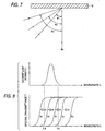
Fig. 7 is a view showing the incidence angle of a light
incident on the optical element for selecting a light.
Fig. 8 is a graph showing, for each incidence angle, the
spectral transmittance of the optical element for selecting
an optical path with respect to the wavelength of the incident
light.
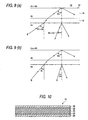
Fig. 9(a) and 9(b) show the views showing an optical path
in the optical element for selecting an optical path.
Fig. 10 is a view showing an example in which the optical
element for selecting an optical path is constituted by a liquid
crystal film.
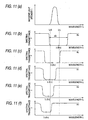
Figs. 11(a) to 11(f) show the graphs showing, for each
incidence angle, a spectral transmittance obtained by the
optical element for selecting an optical path in Fig. 10 with
respect to the wavelength of the incident light.
Fig. 12 is a view showing the structure of an optical
device according to a variant of the first embodiment.
Fig. 13 is a view showing the structure of an optical
device according to a second embodiment.
Fig. 14 is a view showing the structure of an optical
device according to a third embodiment.
Fig. 15 is a view showing a difference in an optical path
for an incidence angle in the case in which a refractive index
of a transparent medium is smaller than a refractive index n3
of the optical element for selecting an optical path.
Fig. 16 is a view showing the difference in an optical
path for the incidence angle in the case in which the refractive
index of the transparent medium is equal to or greater than
that of the optical element for selecting an optical path.
Fig. 17 is a view showing the structure of an optical
device according to a fourth embodiment.
Fig. 18 is a view showing the structure of an optical
device according to a fifth embodiment.
Fig. 19 is a view showing the structure of an optical
device according to a sixth embodiment.
Fig. 20 is a view showing the structure of an optical
device according to a seventh embodiment.
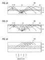
Fig. 21 is a view showing the structure of an optical
device according to a variant of the seventh embodiment.
Fig. 22 is a view showing the structure of an optical
device according to an eighth embodiment.
Figs. 23(a) and 23(b) show the views showing the structure
of an optical device according to a ninth embodiment.
Fig. 24 is a view showing the structure of an optical
device according to a tenth embodiment.
Fig. 25 is a view showing the conceptual whole structure
of the optical device in Fig. 24.
Fig. 26 is a view showing the structure of an optical
device according to an eleventh embodiment.
Fig. 27 is a view showing an example of a structure of
the optical device according to the invention.
Fig. 28 is a graph showing the wavelength band of an
incident light.
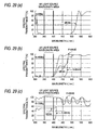
Figs. 29(a) to 29(c) show the graphs showing a change
in a spectral transmittance for a wavelength every incidence
angle.
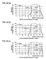
Figs. 30(a) to 30 (c) show the graphs showing the spectral
transmittance for the incidence angle every wavelength.
Figs. 31(a) to 31(c) show the views showing a state in
which an incident light is introduced from a general light
guiding plate and waveguide according to the conventional art.
In the drawings, 10 denotes an optical element for changing
an optical path, 12 denotes an optical element for selecting
an optical path, 14 denotes a transparent medium, 16 denotes
a transparent medium (air), 20 denotes a substance having a
different refractive index, 22 denotes an interface, 26 denotes
a transparent electrode, 28 denotes an oriented layer, 30 denotes
a cholesteric liquid crystal layer, 32 denotes an intermediate
transparent medium, 34 and 35 denote a transparent medium, 36
denotes an optical connecting medium, 38 denotes a medium, 40
denotes a reflector, 42 denotes a light source, 44 denotes a
transparent base material, 46 denotes a transmission type
refractive grating, 48 denotes a medium, 50 denotes a microprism
array, 52 denotes a total reflecting surface, 54 denotes a prism,
56 denotes a transparent medium, 58 denotes a total reflecting
surface, 60 denotes a transparent base material, 62 denotes
a transmission type diffraction grating, 100, 200, 300, 400,
500, 600, 700, 800, 900, 1000, 1100, 1200 and 1300 denote an
optical device, A and B denote an optical path, n denotes a
refractive index (a mean refractive index), n1 denotes a
refractive index of the transparent medium 14, n2 denotes a
refractive index of the transparent medium 16, n3 denotes a
refractive index of the optical element 12, n4 denotes a
refractive index of the transparent medium 34, n5 denotes a
refractive index of the medium 38, n7 denotes a refractive index
of the microprism array 50, n8 denotes a refractive index of
the transparent medium 56, ne denotes an extraordinary index,
no denotes an ordinary index, P denotes a spiral pitch, T denotes
a spectral transmittance, α denotes a vertical angle, Δn
denotes a double refractive index, Δλ denotes a reflecting
wavelength width, , 0, 1, 2 and 3 denote an incidence angle,
c denotes a total reflecting critical angle, and λ denotes
a wavelength.
Best Modes for Carrying Out the Invention
Preferred embodiments of an optical device according to
the invention will be described below in detail with reference
to the drawings.
Fig. 1 shows a schematic structure according to a first
embodiment of the optical device of the invention. An optical
device 100 according to the embodiment has a multilayer structure
in which an optical element 10 for changing an optical path,
an optical element 12 for selecting an optical path and a
transparent medium 14 are provided in this order from the
introduction side of an incident light. A transparent medium
16 is present in the front part of the optical path of the
transparent medium 14 in the optical device 100, and the
relationship between a refractive index n1 (a first refractive
index) of the transparent medium 14 and a refractive index n2
(a second refractive index) of the transparent medium 16 is
set to satisfy total reflecting conditions on an interface 22
of the transparent medium 14 and the transparent medium 16.
More specifically, the transparent medium 14 can be constituted
by a glass substrate (n1 = 1.5) and the transparent medium 16
can be constituted as air (n2 = 1.0), for example. Each layer
constituting the optical device 100 is not substantially
absorbed into the wavelength area of the incident light but
suppresses the incident light and the loss of the incident light
which is totally reflected by the interface 22, thereby
constituting an optical device having a high efficiency.
The optical element 10 for changing an optical path serves
to change the optical path by utilizing a refraction, a
diffraction, a light diffusion and a light reflection, and the
following kinds of optical elements can be used as an example.
In the case in which the refraction is to be utilized, a lens
array, a prism array and a refractive index dispersion member
can be used and the intensity of the incident light is not reduced
substantially. In the case in which the diffraction is to be
utilized, a transmission type diffraction grating shown in Fig.
2 is used, and a phase modulation type diffraction grating such
as a volume hologram (see Fig. 2(a)), a relief type diffraction
grating (see Fig. 2(b)) or a refractive index modulation type
diffraction grating (see Fig. 2(c)) and an amplitude modulation
type diffraction grating can be used to set the angle of an
optical path for an incident light with high precision. Each
optical element can be mass-transferred and produced by a
photopolymer method or an injection molding method, for example.
In the case in which the light diffusion is to be utilized,
moreover, a light diffusing plate shown in Fig. 3 is used and
examples thereof include a porous member (see Fig 3(a)), a
heterorefractive index distribution member and dispersion
member in which a material 20 having a different refractive
index is distributed and dispersed (see Fig. 3(b)), and a light
diffusion member or scattering member having a concavo-convex
surface (see Fig. 3(c)). In the case in which the light
reflection is to be utilized, a distribution member of a
microreflector to carry out a reflection in an optional direction
is used. Any optical element is suitable for mass production
so that a cost can easily be reduced.
In the optical element 12 for selecting an optical path,
the substantially whole selected and transmitted light emitted
from the optical element 12 has a greater angle component than
a total reflecting critical angle in a layer provided in the
front part of an optical path for an incident light, and incident
lights having other angle components are selectively reflected
and are not transmitted. More specifically, only an incident
light having a greater angle component than a total reflecting
critical angle c to be such a condition as to generate a total
reflection on an interface of the transparent medium 14 and
the transparent medium 16 is transmitted through the optical
element 12 for selecting an optical path and incident lights
having other angle components are shielded. The total
reflecting critical angle c is calculated by an equation (1).
c = sin-1(n2/n1)
Specific examples of the optical element 12 for selecting
an optical axis include a light interference filter comprising
a dielectric multilayer film. Fig. 4 shows the layer structure
of the light interference filter.
The light interference filter is a dielectric multilayer
film constituted by-sequentially providing TiO2 and SiO2, and
an optical characteristic thereof has the function of
selectively reflecting an incident light based on a wavelength
thereof which will be described below in detail, and has such
a characteristic that a wavelength to be selectively reflected
depending on an incidence angle is shifted toward the
short-wavelength side. When the wavelength area of the incident
light is represented by λiS to λiL (λiS < λiL), all substantial
incident lights having the wavelength areas λiS to λiL are
selectively reflected for a light including an angle component
having the output angle of the selected and transmitted light
emitted from the optical element 12 which is equal to or smaller
than the total reflecting critical angle c. According to the
structure, an optional wavelength selecting reflective film
can be formed with a large area and a simple structure, and
the optical element 12 for easily selecting an optical path
can be formed by utilizing the incidence angle dependency of
the reflection wavelength. The light interference filter may
be a metal / dielectric multilayer film in which a metal film
is added to the layer structure of the dielectric multilayer
film. The light interference filter comprising the dielectric
multilayer film can be formed by providing, as films, a plurality
of thin film materials on a transparent support substrate by
EB evaporation (electron beam coevaporation) or sputtering.
Moreover, the thin film material may be an organic multilayer
film having a different refractive index or an organic multilayer
film containing an inorganic matter, and can be formed at a
lower cost by coating or laminating in this case.
Detailed description will be given to the optical element
for changing an optical path and the optical property of the
optical element for selecting an optical path.
First of all, there will be supposed the case in which
the optical element for changing an optical path serves to change
the optical path by a refraction, for example. As shown in
Fig. 5, in the case of an optical device in which an optical
element for changing an optical path (a mean refractive index
nt), an optical element for selecting an optical path (a mean
refractive index ns), a transparent medium u (a mean refractive
index nu), a transparent medium v (a mean refractive index nv),
and a transparent medium w on the forward side of a total
reflecting surface (a mean refractive index nw) are provided
in this order, the relationship between an incidence angle on
each interface and the mean refractive index of each medium
is represented as follows if the interface of the transparent
medium v and the transparent medium w is a total reflecting
surface.
nv · sinv = nw
nu · sinu = nv · sinv = nw
ns · sins = nu · sinu = nw
nt · sint = ns · sins = nw
wherein t, s, u and v represent an optical path angle
in each medium. Accordingly, it is necessary to include at
least a light having an angle t to satisfy the following
condition as the condition of the optical element for changing
an optical path and to output the light in a forward direction.
sint > nw/nt
Preferably, the light having the angle t to satisfy the
condition is included as much as possible and is output in the
forward direction. If the transparent medium w is air, nw =
1 is obtained and the condition described above is set as follows.
sint > 1/nt
On the other hand, the condition of the optical element
for selecting an optical path is set to transmit only a light
satisfying the following condition.
sins > nw/ns
If the transparent medium w is the air, nw = 1 is obtained and
the condition described above is set as follows.
sins > 1/ns
A light to be irradiated like a plane is used for an incident
light on the optical device 100, and any of a collimated light
and a diffused light can be used. Moreover, the light may be
incident from the outside of the optical device and may be
incident to have a light source therein. In the case of the
collimated light, an incident light having a specific incidence
angle component can be supplied to the optical device 100 and
a light utilization efficiency can be enhanced. On the other
hand, in the case of the diffused light, the incident light
can be introduced into the optical device 100 in various
directions and an optional plane light source taking a low cost'
can be used. In the case in which a light source is provided
on the inside, moreover, a light emitted from the light source
is directly introduced into the optical device 100 and the
optical device and the light source can be formed integrally
so that a size and a thickness can be reduced and a light
introduction efficiency can be enhanced. On the other hand,
in the case in which the light source is provided on the outside,
the degree of freedom of a design of the optical device 100
can be enhanced and an optional external plane light source
having a large size can also be utilized so that an output can
easily be increased.
Fig. 6 collectively shows the configurations of the
incident light. As shown in Fig. 6, it is possible to use,
for the incident light, a collimated light ranging within a
specific incidence angle or having one or more incidence angles
or a diffused light to be an incident light in an optional
direction. Moreover, it is possible to use, for each of the
collimated light and the diffused light, a light which is
incident like a plane from the outside of the optical device
in the front part of the optical path of the optical device
using the optical device and the light source separately or
a light which is integrated in such a state as to provide a
light source in the front part of the optical path of the optical
device and is incident like a plane.
It is possible to use, for the incident light, a light
having a wavelength in a specific band, for example, a UV light,
a visible light such as a blue light or a green light, and an
infrared light. In the case in which the infrared light is
used, particularly, the effect of blocking a heat wave can also
be obtained. Therefore, it is possible to obtain a convenience
such as the prevention of overheat in respect of practical use.
For the type of the light source, moreover, it is possible
to use a discharge lamp which is generally used and can be exactly
utilized, for example, a fluorescent lamp, a mercury lamp, a
neon tube lamp or a Crookes tube to be an electronic tube which
is charged with an inactive gas or a mercury vapor, a laser
beam source from which a collimated light can easily be obtained,
an LED which is inexpensive and has a defined wavelength area,
an inorganic or organic EL from which a planar light can be
obtained, an incandescent lamp capable of fetching an optical
wavelength component by emitting and filtering a white light
to answer the purpose, a cathode-ray lamp to be a cathode-ray
display tube such as a CRT from which a planar light to be
introduced into the optical device can be directly obtained
and an FED (field emission display) to be a planar display tube
from which a planar light can be directly obtained.
Next, the characteristic of the optical element 12 for
selecting an optical path will be described in detail with
reference to Figs. 7 to 9.
Fig. 7 shows the incidence angle of a light which is
incident on the optical element 12, Fig. 8 is a graph showing,
for each incidence angle, the spectral transmittance of the
optical element 12 for the wavelength of an incident light,
and Fig. 9 is a view showing an optical path on the inside and
outside of the optical element 12.
First of all, there will be supposed the case in which
a light is incident on the optical element 12 at incidence angles
0, 1, 2 and 3 as shown in Fig. 7. As shown in Fig. 8,
the spectral transmittance of the optical element 12 is changed.
More specifically, if the incidence angle is represented by
0 (zero degree) which is equal to or smaller than a total
reflecting critical angle c, the spectral transmittance is
approximately 0% with respect to the wavelength areas λiS to
λiL of the incident light so that a light shielding state (in
which a light is not transmitted but reflected) is brought.
On the other hand, if the incidence angle is greater than the
total reflecting critical angle c, the transmitting
characteristic of the spectral transmittance is shifted toward
the short-wavelength side so that the amount of a transmitted
light is increased when the incidence angle is increased in
order of 1, 2 and 3. In other words, when the incidence
angle of the light incident on the optical element 12 for
selecting an optical path is reduced with respect to the surface
of the optical element 12, the wavelength of the incident light
which is selectively reflected is shifted toward the
short-wavelength side. Consequently, a light having an
incidence angle component 0 of the incident light is not
transmitted and lights having greater incidence angle
components 1, 2 and 3 than a specific angle are transmitted
with an increase in an amount in this order. Therefore, the
optical element 12 is designed to have such a spectral
characteristic that only a greater incident light component
than a total reflecting critical angle c on a predetermined
interface is transmitted. Consequently, an incident light
component which does not satisfy total reflecting conditions
can be shielded and only an incident light component for a total
reflection can be selectively emitted from the optical element
12.
With reference to Fig. 9, description will be given to
an optical path for an incident light in the case in which the
optical device 100 is constituted by using the optical element
12 designed to transmit only a greater incident light component
than the total reflecting critical angle c on the interface
22 as mentioned above.
Fig. 9(a) shows an optical path A in which a light incident
on the optical element 12 for selecting an optical path is
reflected by the optical element 12, and an optical path B in
which the light incident on the optical element 12 for selecting
an optical path is transmitted through the optical element 12
and is totally reflected by the interface 22 of the transparent
medium 14 and the transparent medium 16 provided in the front
part of the optical path.
The optical path A is used when an incidence angle i
of the incident light is equal to or smaller than the total
reflecting critical angle c on the interface 22, and the optical
element 12 does not transmit a light having the incidence angle
component but selectively reflects the same light by a surface
thereof. For this reason, the light having an incidence angle
component which is equal to or smaller than the total reflecting
critical angle c is shielded against the front part of the
optical path by means of the optical element 12.
The optical path B is used when the incidence angle i
of the incident light is greater than the total reflecting
critical angle c on the interface 22, and the optical element
12 transmits a light having the incidence angle component. For
this reason, the light having a greater incidence angle component
than the total reflecting critical angle c is transmitted
through the optical element 12 and is introduced into the
transparent medium 14, and is totally reflected by the interface
22.
Fig. 9(a) shows the case in which a refractive index na
on the side on which the light is incident and a refractive
index nb of the transparent medium 14 are equal to each other,
and the incidence angle i for the optical element 12 and the
angle s on the interface 22 are equal to each other.
On the other hand, Fig. 9(b) shows the case in which the
refractive index na on the side on which the light is incident
and the refractive index nb of the transparent medium 14 are
different from each other, and the incidence angle i for the
optical element 12 and the incidence angle s on the interface
22 are different from each other. In this case, the optical
element 12 is designed such that the incidence angle s on the
interface 22 is greater than the total reflecting critical angle
c.
The optical device 100 is constituted by using the optical
element 12 for selecting an optical path which is designed as
described above. Consequently, when a planar incident light
comprising the collimated light or the diffused light introduced
from the inside or outside of the optical device 100 is incident
on the optical element 10 for changing an optical path as is
indicated by an optical path shown in an arrow of Fig. 1, the
optical path is changed through a diffusion from the irradiation
position of the light. When a light having an optical path
changed reaches the optical element 12 for selecting an optical
path, only the incident light having a greater angle component
than the total reflecting critical angle c on the interface
22 of the transparent medium 14 and the transparent medium 16
is transmitted through the optical element 12 and incident lights
having other angle components are reflected by the surface of
the optical element 12 toward the light incident side.
Accordingly, only a light to be reflected totally by the
interface 22 of the transparent medium 14 and the transparent
medium 16 which is incident on the optical device 100 is
introduced into the front part of the optical path, and the
light thus introduced is totally reflected by the interface
22 to be a face in the frontmost part of the optical path for
the incident light in the optical device 100. More specifically,
in the optical element 12 for selecting an optical path, the
substantially whole transmitted light emitted from the optical
element 12 has a greater angle component than a total reflecting
critical angle on an interface in the front part of the optical
path for the incident light of the interface of layers provided
in the front part of the light path for the incident light through
the optical element 12 for selecting an optical path, and
incident lights having other angle components are selectively
reflected and are not transmitted. In a medium having a total
reflecting surface, light guiding, storage and containment are
not substantially carried out.
Moreover, a part of the light reflected toward the light
incident side by the surface of the optical element 12 for
selecting an optical path is reflected at the light incident
side of the optical element 10 for changing an optical path,
and is transmitted into the optical element 12 for selecting
an optical path again. The light thus transmitted again has
an incidence angle increased to be greater than the total
reflecting critical angle c, and is thus transmitted through
the optical element 12 and is introduced into the transparent
medium 14.
According to the optical device 100 in accordance with
the embodiment, thus, the incident light is directly and
efficiently introduced like a plane from the planar light source
into the optical device 100 without using a light guiding plate
or an optical waveguide. As compared with the case in which
the light is incident from the end face side, therefore, an
introduction port for the incident light can be considerably
enlarged and a coupling efficiency with the incident light can
be enhanced so that a planar total reflected light can be obtained
efficiently without an influence by a reduction in the thickness
of the optical device 100 itself. Moreover, an increase in
the output of the optical device 100 can be achieved easily.
Furthermore, at least a part of the incident light introduced
into the optical device by a reflector having no absorption
without depending on an incidence angle is reflected by a total
reflection having no reflection loss. Therefore, the optical
device can be caused to function as a reflector having a high
efficiency. Since a part of the incident light reflected by
each interface in the optical device is transmitted again into
the front part of the optical path, and furthermore, the light
transmitted from the optical device is not substantially
generated, a light utilization efficiency can be enhanced.
Consequently, it is possible to increase an application range
to an optical device and an optical system which utilize the
total reflection of the optical device. A gas contact interface
on which the optical device 100 comes in contact with air (which
may be an inactive gas) is set to be a total reflecting surface
so that the total reflection can be generated with a simple
structure without separately providing a layer having such a
refractive index as to generate the total reflection.
In the embodiment, moreover, the optical element for
changing an optical path is provided in optical contact with
the optical element for selecting an optical path. Therefore,
both light coupling properties can be enhanced. In addition,
in the case in which the optical element for changing an optical
path has a directivity, the incident light can be introduced
from the optical element for changing an optical path into the
optical element for selecting an optical path with the incidence
angle component held.
Next, description will be given to another example of
a structure in which a Bragg reflecting filter is used as the
optical element 12 for selecting an optical path in place of
the light interference filter.
Fig. 10 shows an example in which the optical element
12 for selecting an optical path is constituted by a liquid
crystal film. In this case, the optical element 12 is
constituted by a pair of transparent electrodes 26 comprising
ITO, an oriented layer 28 formed on the inside thereof, and
a cholesteric liquid crystal layer 30 surrounded by the oriented
layer 28.
The filtering effect of the cholesteric liquid crystal
layer 30 having such a structure will be described below. The
cholesteric liquid crystal layer 30 has a cholesteric liquid
crystal molecule oriented in parallel with a layer, and presents
a spiral structure in the vertical direction to the layer.
A double refractive index Δn can be expressed in an
equation (2), wherein an ordinary index, an extraordinary index,
a double refractive index and a mean refractive index in the
cholesteric liquid crystal layer 30 are represented by no, ne,
Δn and n, respectively.
Δn = ne - no
Moreover, the mean refractive index n is approximately
expressed in an equation (3).
n = (ne + no)/2
Furthermore, in the case in which the spiral pitch of
the cholesteric liquid crystal layer 30 is represented by P [nm],
the cholesteric liquid crystal layer 30 indicates such a
characteristic as to selectively carry out a reflection in the
principle of a Bragg reflection. More specifically, in the
case in which a light incident on the cholesteric liquid crystal
layer 30 at an incidence angle [deg] is selectively reflected,
a central wavelength λ()[nm] of the incident light can be
expressed in an equation (4).
λ() = λ(0) · cos[sin-1(sin/n)]
The incident light is incident from air (a refractive
index = 1). The λ(0)[nm] represents a central wavelength with
an incidence angle 0, that is, when the light is incident
vertically to a layer, and can be expressed in an equation (5).
λ(0) = n · P
Moreover, a reflection wavelength width Δλ[nm] can be
expressed in an equation (6).
Δλ = Δn · P
Accordingly, the ordinary index no, the extraordinary
index ne and the spiral pitch P which are the physical property
values of the cholesteric liquid crystal layer 30 are controlled
to form a layer. Consequently, it is possible to form an optical
filter having an optional reflecting central wavelength λ()
to be changed depending on the incidence angle and a desirable
reflecting wavelength width Δλ. For example, the spiralpitch
P can be regulated by a manufacturing method for mixing and
preparing at least two kinds of materials havingdifferent spiral
pitches.
In the case in which the wavelength area of an incident
light to be an object is large, furthermore, it is also necessary
to enlarge the selecting reflection wavelength area of the
cholesteric liquid crystal layer. In this case, it is possible
to enlarge the reflecting wavelength area by orienting a liquid
crystal in such a manner that the spiral pitch is continuously
varied in the direction of a thickness. Moreover, it is also
possible to enlarge the reflecting wavelength area by laminating
the cholesteric liquid crystal layers in the different selecting
reflection wavelength areas.
The cholesteric liquid crystal layer 30 can be
manufactured in the following manner.
A polyimide oriented film is coated on a support member
for forming a cholesteric liquid crystal and is then dried,
and a surface treatment is carried out by rubbing. Consequently,
the polyimide oriented film is formed. The polyimide oriented
film is coated with a prepared solution having a mixture of
a low molecular cholesteric liquid crystal or a nematic liquid
crystal and a chiral agent causing a twist, a polymeric monomer
and a photopolymerization initiator which are mixed with an
organic solvent, and orientation is then carried out at a proper
temperature. Thereafter, an ultraviolet radiation is exposed
to a necessary portion and is photopolymerized, and an
unnecessary portion is removed by a development. Finally, high
temperature baking is carried out to obtain a stabilization.
In order to control the direction of the twist and the
reflecting incidence angle, it is preferable that the
cholesteric liquid crystal, the chiral agent and each
concentration should be changed appropriately.
Moreover, it is also possible to form a film by using
a polymeric cholesteric liquid crystal. In this case, in the
same manner as described above, the polyimide oriented film
is coated with a prepared solution in which a polymeric
cholesteric liquid crystal and a photopolymerization initiator
are mixed with an organic solvent and an orientation is then
carried out at a proper temperature, and an ultraviolet radiation
is exposed to a necessary portion and is photopolymerized. A
reflecting incidence angle can be controlled by properly
selecting an orientation temperature and a stabilization can
be obtained by the photopolymerization.
Fig. 11 shows the spectral transmittance of the optical
element 12 for selecting an optical path having the structure
described above. In this example, a cholesteric liquid crystal
layer is obtained by superposing a left twisted cholesteric
liquid crystal layer and a right twisted liquid crystal layer
and a total polarizing component is reflected in a reflection
wavelength area. In the case in which the incidence angle is
represented by 0 which is equal to or smaller than the total
reflecting critical angle c (see Fig. 7), the spectral
transmittance is approximately 0% with respect to the wavelength
areas λiS to λiL of the incident light so that a light shielding
state is brought. When the incidence angle is greater than
the total reflecting critical angle c and is increased in order
of 1, 2 and 3, the transmitting characteristic of the
spectral transmittance is shifted toward the short-wavelength
side so that the amount of a transmitted light is increased.
Consequently, an incident light having an incidence angle
component 0 is not transmitted but lights having incidence
angle components 1, 2 and 3 which are greater than a specific
angle are transmitted with an increase in an amount in this
order. By carrying out a design to have the spectral
characteristic of the optical element 12 such that only a greater
incident light component than the total reflecting critical
angle c on a predetermined interface is transmitted, an
incident light component which does not satisfy total reflecting
conditions can be removed selectively and only an incident light
component to be totally reflected can be emitted from the optical
element 12.
According to the structure, it is possible to obtain the
same functions and effects as those in the case in which the
light interference filter is used, and the optical element 12
for selecting an optical path can be implemented at a low cost.
Referring to the cholesteric liquid crystal layer 30,
moreover, in the case in which the spiral structure has a right
twist, a light having a right circular polarizing component
is reflected and a light having a left circular polarizing
component along a spiral is transmitted. On the other hand,
in the case in which the spiral structure has a left twist,
the light having the left circular polarizing component is
reflected and the light having the right circular polarizing
component is transmitted. In the case in which a light having
a total polarizing component is reflected, that is, is not
transmitted, accordingly, a total polarized light can be
reflected by such a structure that a left twisted (or right
twisted) cholesteric layer and the right twisted (or left
twisted) cholesteric layer which is reverse thereto are
sequentially superposed.
In addition to the cholesteric liquid crystal, a volume
hologram is effective for the optical element having the function
of the Bragg reflection. The volume hologram has the Bragg
reflecting function by a grating-shaped refractive index
distribution formed in a film, and serves to reflect a specific
wavelength. Moreover, when an incidence angle is increased,
the wavelength to be reflected is shifted toward the
short-wavelength side and the volume hologram functions as an
optical path selecting film. The volume hologram can be formed
by using, as a photosensitive material, a photographic sensitive
material for a hologram, a phase separation type photopolymer,
an HPDLC (a holographic polymer dispersing liquid crystal) or
a photolithography material and carrying out multiple beam
interference exposure thereto.
Next, description will be given to a variant of the optical
device 100 according to the embodiments Fig. 12 is a view showing
the structure of an optical device 200 according to the variant
of the embodiment, in which an incident light is present in
the optical device 200. In other words, a light source is
provided in the optical device 200 in the structure. More
specifically, there are a structure in which a light source
is sealed with a resin in the optical device 200 and a structure
in which an optical element 10 itself for changing an optical
path is a light emitting element. In this case, an incidence
angle may be a predetermined angle or an optional angle.
According to the variant, an incident light is diffused
by the optical element 10 for changing an optical path and is
then irradiated on the optical element 12 for selecting an
optical path in various incidence directions. Thereafter, the
optical element 12 for selecting an optical path selectively
transmits only an incident light having an angle component to
be totally reflected by an interface 22 and reflects incident
lights having other angle components. Consequently, it is
possible to obtain the same functions and effects as described
above.
In the structures of the optical device 100 according
to the first embodiment and the optical device 200 according
to the variant, a transparent medium 14 may be provided in the
rear part of the optical path of the optical element 10 for
changing an optical path. In this case, an interface generating
a total reflection is set to be an interface in the front part
of the optical path of the optical element 12 for selecting
an optical path. Thus, it is preferable that the optical device
should have the optical element 10 for changing an optical path
and the optical element 12 for selecting an optical path provided
in this order from the rear part of the optical path toward
the front part thereof, and an optional medium such as a
transparent medium maybe provided between the laminated layers.
Next, description will be given to a second embodiment
of the optical device according to the invention.
Fig. 13 shows the structure of an optical device 300
according to the embodiment. The optical device 300 according
to the embodiment has a multilayer structure in which an optical
element 10 for changing an optical path, an intermediate
transparent medium 32 having a refractive index of a glass
substrate which is greater than 1, and an optical element 12
for selecting an optical path are provided in this order from
the introduction side of an incident light. A transparent
medium 16 is present in the front part of the optical path of
the optical element 12 for selecting an optical path in the
optical device 300, and the relationship between a refractive
index n3 of the optical element 12 and a refractive index n2
of the transparent medium 16 is set to satisfy total reflecting
conditions on the interface of the optical element 12 and the
transparent medium 16. Moreover, the incident light may be
present on the outside or inside of the optical device 300,
and may be a collimated light or a diffused light.
According to the optical device 300, the incident light
is diffused by the optical element 10 for changing an optical
path and is then irradiated on the optical element 12 for
selecting an optical path through the intermediate transparent
medium 32 in various incidence directions. The refractive index
of each medium is properly regulated or a reflection preventing
treatment is carried out on each interface such that a total
reflection is not substantially generated on an interface with
the intermediate transparent medium 32. Thereafter, only a
light having an incidence angle component to be totally reflected
in the optical element 12 for selecting an optical path in the
incident light is transmitted through the optical element 12
and the transmitted light is totally reflected by an interface
24 of the optical element 12 for selecting an optical path and
the transparent medium 16, while an incident light component
which does not satisfy the total reflecting conditions is
reflected in the front part of the optical path of the optical
element 12 for selecting an optical path. Consequently, it
is possible to obtain the same functions and effects as described
above.
Next, description will be given to a third embodiment
of the optical device according to the invention.
Fig. 14 shows the structure of an optical device 400
according to the embodiment. The optical device 400 according
to the embodiment has a multilayer structure in which an optical
element 10 for changing an optical path, an intermediate
transparent medium 32 having a refractive index of a glass
substrate which is greater than 1, an optical element 12 for
selecting an optical path which has a mean refractive index
of n3 and a transparent medium 34 having a refractive index
of n4 are provided in this order from the introduction side
of an incident light, and the transparent medium 34 such as
a transparent thin film is provided in the front part of the
optical path of the incident light in the optical device 300
according to the second embodiment. The transparent medium
16 is present in the front part of the optical path of the
transparent medium 34 in the optical device 400, and the
relationship between the refractive index n4 of the transparent
medium 34 and a refractive index n2 of the transparent medium
16 is set to satisfy total reflecting conditions on the interface
of the transparent medium 34 and the transparent medium 16.
Moreover, the incident light may be present on the outside or
inside of the optical device 400 and may be a collimated light
or a diffused light.
According to the optical device 400 in accordance with
the embodiment, the incident light is diffused by the optical
element 10 for changing an optical path and is then irradiated
on the optical element 12 for selecting an optical path through
the intermediate transparent medium 32 in various incidence
directions. Thereafter, only a light having an incidence angle
component to be totally reflected by an interface 25 of the
transparent medium 34 and the transparent medium 16 is
transmitted by the optical element 12 for selecting an optical
path and the transmitted light is totally reflected by the
interface 25 of the transparent medium 34 and the transparent
medium 16, while an incident light component which does not
satisfy the total reflecting conditions is reflected in the
front part of the optical path of the optical element 12 for
selecting an optical path. Consequently, it is possible to
produce the same functions and effects as described above.
By regulating the refractive index of the transparent
medium 34, it is possible to set an interface generating the
total reflection into the front part of the optical path of
the transparent medium 34 or into the interface of the optical
element 12 for selecting an optical path and the transparent
medium 34.
The reflecting conditions of the
transparent medium 34
will be described below. Fig. 15 is a view showing a difference
in an optical path for an incidence angle in the case in
which the refractive index n4 of the
transparent medium 34 is
smaller than the refractive index n3 of the
optical element
12 for selecting an optical path, and the incidence angle
is gradually increased in order of (a) to (c). The light is
reflected by the interface of the
optical element 12 for
selecting an optical path and the transparent medium 34 in the
(a) in which the incidence angle is small, the light is
transmitted through the interface and is totally reflected in
the front part of the optical path of the transparent medium
34 in the (b), and the light is totally reflectedby the interface
in the (c) in which the incidence angle is great. At this
time, an incidence angle condition in each state is as follows.
Moreover, Fig. 16 shows a difference in the optical path
for the incidence angle in the case in which the refractive
index n4 of the
transparent medium 34 is equal to or greater
than the refractive index n3 of the
optical element 12 for
selecting an optical path. In this case, the light is not totally
reflected by the interface of the
optical element 12 for
selecting an optical path and the
transparent medium 34.
Similarly, the incidence angle condition in each state is as
follows.
By appropriately regulating the refractive index of the
transparent medium 34 depending on the situation of use of the
optical device, accordingly, it is possible to set the interface
generating the total reflection into the front part of the
optical path of the transparent medium 34 or the interface of
the optical element 12 for selecting an optical path and the
transparent medium 34 and it is possible to optionally set the
interface generating the total reflection.
The transparent medium 34 according to the embodiment
may be provided as a protective film for preventing the external
damage or deterioration of the optical element 12 for selecting
an optical path or may be a film having other functions, for
example, a film having optical or electrical functions.
Moreover, the transparent medium 34 may be constituted by a
plurality of films.
The multipurpose transparent medium 34 may be provided
in the front part of the optical path of the transparent medium
16 in the optical device 100 according to the first embodiment
shown in Fig. 1. Also in this case, it is possible to obtain
the same effects as described above.
Next, description will be given to a fourth embodiment
of the optical device according to the invention.
Fig. 17 shows the structure of an optical device 500
according to the embodiment. The optical device 500 according
to the embodiment has a multilayer structure in which an optical
element 10 for changing an optical path, an optical connecting
medium 36 such as an adhesive layer, an optical element 12 for
selecting an optical path and a transparent medium 14 such as
a glass substrate are provided in this order from the
introduction side of an incident light, and the optical
connecting medium 36 is provided between the optical element
10 for changing an optical path and the optical element 12 for
selecting an optical path in the optical device 100 according
to the first embodiment. A transparent medium 16 is present
in the front part of the optical path of the transparent medium
14 in the optical device 500, and the relationship between a
refractive index n4 of the transparent medium 14 and a refractive
index n2 of the transparent medium 16 is set to satisfy total
reflecting conditions on an interface 22 of the transparent
medium 14 and the transparent medium 16. Moreover, an incident
light may be present on the outside or inside of the optical
device 500 and may be a collimated light or a diffused light.
According to the optical device 500 in accordance with
the embodiment, the incident light is diffused by the optical
element 10 for changing an optical path and is then introduced
through the optical connecting medium 36 into the optical element
12 for selecting an optical path in various incidence directions.
Thereafter, only a light having an incidence angle component
to be totally reflected by the interface of the transparent
medium 14 and the transparent medium 16 in the front part of
the optical path is transmitted by the optical element 12 for
selecting an optical path and the transmitted light is totally
reflected by the interface 22 of the transparent medium 14 and
the transparent medium 16, while an incident light component
which does not satisfy the total reflecting conditions is
reflected in the front part of the optical path of the optical
element 12 for selecting an optical path. Consequently, it
is possible to obtain the same functions and effects as described
above.
The multipurpose transparent medium 34 according to the
third embodiment may be provided in the front part of the optical
path of the transparent medium 14 according to the embodiment.
Also in this case, it is possible to obtain the same effects
as described above. By regulating the refractive indices of
the transparent medium 34 and the transparent medium 14, it
is possible to set a total reflecting surface into the front
part of the optical path of the transparent medium 34 or the
interface of the transparent medium 14 and the transparent medium
34.
Next, description will be given to a fifth embodiment
of the optical device according to the invention.
Fig. 18 shows the structure of an optical device 600
according to the embodiment. The optical device 600 according
to the embodiment has a multilayer structure in which an optical
element 10 for changing an optical path, an optical connecting
medium 36 such as an adhesive layer, an optical element 12 for
selecting an optical path, a transparent medium 14 such as a
glass substrate and a medium 38 having a smaller refractive
index n5 than a refractive index n1 of the transparent medium
14 are provided in this order from the introduction side of
an incident light, and the medium 38 having a lower refractive
index is provided in the front part of an optical path for an
incident light in the optical device 500 according to the fourth
embodiment. The relationship between a refractive index n1
of the transparent medium 14 and a refractive index n5 of the
medium 38 in the optical device 600 is set to satisfy total
reflecting conditions on an interface 39 of the transparent
medium 14 and the medium 38. Moreover, an incident light may
be present on the outside or inside of the optical device 500
and may be a collimated light or a diffused light.
According to the optical device 600 in accordance with
the embodiment, the incident light is diffused by the optical
element 10 for changing an optical path and is then introduced
through the optical connecting medium 36 into the optical element
12 for selecting an optical path in various incidence directions.
Thereafter, only a light having an incidence angle component
to be totally reflected by an interface 39 of the transparent
medium 14 and the medium 38 in the front part of the optical
path is transmitted by the optical element 12 for selecting
an optical path and the transmitted light is totally reflected
by the interface 39 of the transparent medium 14 and the medium
38. On the other hand, an incident light component which does
not satisfy the total reflecting conditions is reflected in
the front part of the optical path of the optical element 12
for selecting an optical path. Consequently, it is possible
to obtain the same functions and effects as described above.
The medium 38 according to the embodiment may be provided
as a protective film for preventing the external damage or
deterioration of the optical element 12 for selecting an optical
path.
Next, description will be given to a sixth embodiment
of the optical device according to the invention.
Fig. 19 shows the structure of an optical device 700
according to the embodiment. The optical device 700 according
to the embodiment is provided with a reflector 40 such as a
diffusion reflector or a specular mirror which is opposed to
the incident light introduction side of the optical device 100
according to the first embodiment to reflect a light, and a
light source 42 is provided between the reflector 40 and the
optical device 100. Accordingly, a light transmitted from the
light source 42 is irradiated from the outside of the optical
device 100. The light may be a collimated light or a diffused
light.
According to the optical device 700 in accordance with
the embodiment, the incident light transmitted from the light
source 42 is irradiated on an optical element 10 for changing
an optical path and is diffused, and is then introduced into
an optical element 12 for selecting an optical path in various
incidence directions. Only a light having an incidence angle
component to be totally reflected by an interface 22 of a
transparent medium 14 and a transparent medium 16 in the front
part of an optical path is transmitted through the optical
element 12 for selecting an optical path, and is totally
reflected by the interface 22 of the transparent medium 14 and
the transparent medium 16. On the other hand, an incident light
component which does not satisfy total reflecting conditions
is reflected by the optical element 12 for selecting an optical
path. The reflected light is transmitted again into the optical
element 12 side for changing an optical path by means of the
reflector 40 and is thus recycled. In the case in which the
light source 42 emits a diffused light, moreover, a light emitted
to the opposite side to the optical element 12 side for changing
an optical path is reflected by the reflector 40 and is thus
recycled. Consequently, the light utilization efficiency of
each of the light source 42 and the optical device 700 can be
enhanced and the light output intensity of the optical device
700 can be increased.
In addition to the foregoing, there are various
combinations of the optical element for changing an optical
path, the optical element for selecting an optical path and
the transparent medium, and furthermore, a total reflecting
interface can also be proposed variously. It is also possible
to employ any combination which does not depart from the scope
of the invention.
Next, description will be given to a seventh embodiment
according to the invention in which an optical device is
constituted by using only the element for selecting an optical
path in the optical element for changing an optical path and
the optical element for selecting an optical path.
Fig. 20 shows the structure of an optical device 800
according to the embodiment. The optical device 800 according
to the embodiment has a multilayer structure in which a
transparent base material 44 such as a glass substrate or a
transparent resin, an optical element 12 for selecting an optical
path and a transparent medium 14 having a total reflecting
surface are provided in this order from the introduction side
of an incident light. A transparent medium 16 is present in
the front part of the optical path of the transparent medium
14 in the optical device 800, and the relationship between a
refractive index n4 of the transparent medium 14 and a refractive
index n2 of the transparent medium 16 is set to satisfy total
reflecting conditions on the interface of a transparent medium
34 and the transparent medium 16. Moreover, an incident light
in this case has already been introduced into the transparent
base material 44 and is thus present. The presence can be
implemented by a structure in which a light is introduced from
another optical path into the transparent base material 44 or
a structure in which a light emitting source is present in the
transparent base material 44.
According to the optical device 800 in accordance with
the embodiment, the incident light introduced into the
transparent base material 44 is irradiated on the optical element
12 for selecting an optical path in various directions. Then,
only a light having an incidence angle component to be totally
reflected by an interface 22 of the transparent medium 14 and
the transparent medium 16 is transmitted by the optical element
12 for selecting an optical path and the transmitted light is
totally reflected by the interface 22 of the transparent medium
14 and the transparent medium 16. On the other hand, an incident
light component which does not satisfy the total reflecting
conditions is reflected in the front part of the optical path
of the optical element 12 for selecting an optical path.
Consequently, it is possible to obtain the same functions and
effects as described above.
It is also possible to employ such a structure that a
medium having a lower refractive index than a refractive index
n1 of the transparent medium 14 is provided in the front part
of an optical path for the incident light of the transparent
medium 14. Also in this case, the incident light introduced
into the optical element 12 for selecting an outward route is
reflected by a total reflection through the interface 22 in
the front part of the optical path of the transparent medium
14.
Next, description will be given to a variant of the optical
device 800 according to the embodiment.
Fig. 21 shows the structure of an optical device 900
according to the variant. The optical device 900 according
to the variant has a structure in which an optical element 12
for selecting an optical path is provided on a transparent medium
35 such as a glass substrate or a transparent resin. A
transparent medium 16 is present in the front part of the optical
path of the optical element 12 for selecting an optical path
in the optical device 900, and the relationship between a
refractive index n3 of the optical element 12 and a refractive
index n2 of the transparent medium 16 is set to satisfy total
reflecting conditions on an interface 24 of the optical element
12 and the transparent medium 16.
According to the optical device 900 in accordance with
the embodiment, the incident light introduced into the
transparent medium 35 is irradiated on the optical element 12
for selecting an optical path in various directions. Then,
only a light having an incidence angle component to be totally
reflected by the interface 24 is transmitted by the optical
element 12 for selecting an optical path and the transmitted
light is totally reflected by the interface 24. On the other
hand, an incident light component which does not satisfy the
total reflecting conditions is reflected in the front part of
the optical path of the optical element 12 for selecting an
optical path. Consequently, it is possible to obtain the same
functions and effects as described above.
Next, description will be given to an embodiment in which
an optical element for selecting an optical path which is used
in the optical device according to each of the first to seventh
embodiments can be implemented with a simple and inexpensive
structure without using a dielectric multilayer film and a
cholesteric liquid crystal film.
First of all, description will be given to an eighth
embodiment of the optical device according to the invention
in which the optical device is constituted by a transmission
type diffraction grating.
Fig. 22 shows the structure of an optical device 1000
according to the embodiment. The optical device 1000 according
to the embodiment has a multilayer structure in which a
transparent base material 44 such as a glass substrate or a
transparent resin, a transmission type diffraction grating 46
and a medium 48 having a total reflecting surface are provided
in this order from the introduction side of an incident light.
The incident light is a planar light ranging within a specific
incidence angle. In the case in which the transmission type
diffraction grating 46 is obtained by multiple hologram
interference exposure, an optional incidence angle maybe set.
While the volume hologram shown in Fig. 2(a) can be
preferably used for the transmission type diffraction grating
46, it is also possible to use the relief type diffraction grating
shown in Fig. 2(b), the refractive index distribution type
diffraction grating shown in Fig. 2(c) or an amplitude modulation
type diffraction grating.
According to the optical device 1000 in accordance with
the embodiment, when a planar incident light to be a collimated
light is irradiated on theoptical device 1000, it is transmitted
through the transparent base material 44 and an optical path
is converted to have such an angle as to generate a total
reflection in the medium 48 through the transmission type
diffraction grating 46. In other words, the transmission type
diffraction grating 46 is designed such that the incident light
has an angle at which the total reflection is generated in the
medium 48. By the transmission type diffraction grating 46,
thus, it is possible to convert the incident light to have such
an angle as to generate the total reflection, thereby generating
the total reflection over the interface of the medium 48 in
the front part of an optical path for the incident light.
Next, description will be given to a ninth embodiment
of the optical device according to the invention in which the
optical device is constituted by using a prism.
Fig. 23 shows the structure of an optical device 1100
according to the embodiment. The optical device 1100 according
to the embodiment comprises a microprism array 50, and Fig.
23 (a) is a plan view showing the microprism array 50 seen from
the incidence surface side of a light and Fig. 23(b) is a sectional
view showing a P - P section in (a).
The microprism array 50 is plate-shaped and has such a
configuration that an upper surface is set to be a flat total
reflecting surface 52 and a lower surface is provided with a
plurality of concavo-convex prisms 54 having a cone-shaped
section in parallel.
Examples of the material of the microprism array 50 include
a glass and a resin, and particularly, the resin is preferable
in respect of mass production. For the resin, acryl based resins,
epoxy based resins, polyester based resins, polycarbonate based
resins, styrene based resins and vinyl chloride based resins
are optically preferable, and furthermore, examples of the resin
material include a photo-curing type, a photo-dissolving type,
a thermosetting type and a thermoplastic type which can be
selected appropriately.
As a method of manufacturing the microprism array 50,
casting using a mold, hot press molding, injection molding,
printing or photolithography is preferable in respect of a
productivity
More specifically, formation can be carried out by
pressing a thermoplastic resin in a microprism-shaped mold.
Moreover, the formation can be carried out by filling the mold
with a photo-curing resin or a thermosetting resin and then
curing the resin through a light or heat and removing the cured
resin from the mold.
For the photolithography, the formation is carried out
by exposing an ultraviolet radiation (or a visible light) to
a photo-dissolving resin or a photo-curing resin through a
shielding mask patterned properly and performing a dissolving
development in the exposedportionor the dissolving development
in an unexposed portion. It is possible to obtain a microprism
having a desirable shape by a resin material and an exposure
amount distribution. Depending on the resin material, moreover,
it is possible to carry out a high temperature baking treatment
after the development, thereby obtaining the microprism array
50 having a desirable shape by a surface tension during
thermosoftening.
Furthermore, the incident light is a planar light ranging
within a specific incidence angle and is incident on the optical
device 1100 at an incidence angle i as shown in Fig. 23(b).
According to the optical device 1100 in accordance with
the embodiment, in the case in which a medium present around
the microprism array 50 is air (a refractive index n2 = 1) and
the microprism array 50 is formed of a transparent resin (a
refractive index n7 = 1.5), a total reflecting critical angle
c on a total reflecting surface 52 is calculated in the same
manner as in the equation (1) to be 42 [deg].
As an example for setting an incidence angle for the
total reflecting surface 52 to be ≧ c, therefore, a vertical
angle α of the prism is set to be approximately 90 [deg] and
a lateral opening angle is set to be approximately 45 [deg].
In this case, when the incident light is incident fromthe outside
of the prism, the incidence angle i of the incident light is
set to be approximately 45 [deg]. Under this condition, an
optical shading is not substantially generated but the incident
light can be totally reflected efficiently by the total
reflecting surface 52. The vertical angle α of the prism is
not restricted thereto.
By using the microprism array 50 which can be mass produced
easily and inexpensively, consequently, it is possible to
introduce an incident light to be irradiated like a plane and
to totally reflect the substantially whole incident light thus
introduced.
Next, description will be given to a tenth embodiment
of the optical device according to the invention in which the
optical device is constituted by using the microprism array
according to the ninth embodiment.
Fig. 24 shows the sectional structure of an optical element
1200 according to the embodiment and Fig. 25 shows the
conceptional whole structure of the optical element 1200. The
optical element 1200 according to the embodiment has a lamination
structure in which a microprism array 50 and a transparent medium
56 such a glass or a resin are provided from the introduction
side of an incident light.
A transparent medium 16 is present in the front part of
the optical path of the transparent medium 56 in the optical
element 1200, and the relationship between a refractive index
n8 of the transparent medium 56 and a refractive index n2 of
the transparent medium 16 is set to satisfy total reflecting
conditions on the interface of the transparent medium 56 and
the transparent medium 16. Moreover, an incident light is a
planar light ranging within a specific incidence angle.
According to the optical element 1200 in accordance with
the embodiment, the planar incident light is irradiated on the
microprism array 50 and an incident light having a predetermaned
incidence angle component set by a vertical angle α of a prism
by means of the microprism array 50 is introduced into the
transparent medium 56. Then, the incident light thus introduced
is totally reflected efficiently by a total reflecting surface
58 of the transparent medium 56.
By using the microprism array 50 which can be mass produced
easily and inexpensively to introduce an incident light to be
irradiated like a plane, thus, it is possible to totally reflect
the substantially whole introduced incident light by the
interface 58 of the transparent medium 56.
Next, description will be given to an eleventh embodiment
of the optical device according to the invention in which an
optical element for changing an optical path at an angle
corresponding to the light incidence angle of a microprism array
50 is provided in the front part of the optical path of the
optical element 1200 according to the tenth embodiment, thereby
constituting the optical device.
Fig. 26 shows the sectional structure of an optical device
1300 according to the embodiment. The optical device 1300
according to the embodiment comprises an optical element having
a transparent base material 60 such as a glass substrate or
a transparent resin and a transmission type diffraction grating
62 provided in this order and the optical element 1200 according
to the tenth embodiment from the introduction side of an incident
light. The incident light is a planar light ranging within
a specific incidence angle.
While a volume hologram can be preferably used for the
transmission type diffraction grating 62 in the same manner
as the transmission type diffraction grating 46 according to
the seventh embodiment, it is also possible to use a relief
type diffraction grating, a refractive index distribution type
diffraction grating or an amplitude modulation type diffraction
grating.
According to the optical device 1300 in accordance with
the embodiment, when a planar incident light to be a collimated
light is irradiated on the optical device 1300, it is transmitted
through the transparent base material 60 and an optical path
is converted into a light having a predetermined incidence angle
component set by a vertical angle α of a microprism array 50
by the transmission type diffraction grating 62. More
specifically, the optical path is converted to have such an
angle as to generate a total reflection by an interface 58 of
a transparent medium 56. In other words, the transmission type
diffraction grating 62 is designed such that an incident light
has an angle at which a total reflection is generated by the
interface 58 of the transparent medium 56. By converting the
incident light to have such a predetermined incidence angle
as to be introduced into the microprism array 50 by the
transmission type diffraction grating 62, thus, it is possible
to totally reflect the introduced incident light by the interface
58 of the transparent medium 56.
The optical device according to the invention described
above can be applied to a reflector such as a visible transparent
film for reflecting an infrared light, a high efficient
reflecting film, a high efficient reflecting film having a
wavelength selectivity or a reflector or film for a light source
having a high efficiency, an indicator such as a decorative
illumination advertisement display utilizing a planar total
reflected light, an optical modulating element and a plane
display, for example.
Description will be given to a specific example of the
structure of the optical device according to the invention and
a result obtained by calculating, through a simulation, the
spectral transmittance of the optical device according to the
example of the structure.
Fig. 27 shows an example of the structure of the optical
device according to the invention. In the optical device in
this case, a light diffusing film (a refractive index n = 1.5)
to be an optical element for changing an optical path, a
dielectricmultilayer film to be an optical element for selecting
an optical path and a glass substrate (a refractive index n
= 1.5) are sequentially provided from the introduction side
of an incident light. Air (a refractive index n = 1.0) is present
in the front part of the optical path of the glass substrate.
The dielectric multilayer film has a 29-layer structure
of TiO2/SiO2/ ... /SiO2/TiO2 and the optical thickness of each
layer is set to be 1/4λ (a wavelength λ = 440 [nm]). Moreover,
a UV light source having a wavelength λ = 350 to 400 [nm] shown
in Fig. 28 was used for the incident light. In this case, a
total reflecting critical angle c is set to be approximately
40 [deg].
The spectral transmittance of an optical device (a
dielectric multilayer film) was calculated under the condition
described above so that results shown in Figs. 29 and 30 were
obtained. Fig. 29 is a graph showing a change in a spectral
transmittance T for the wavelength λ every incidence angle
and Fig. 30 is a graph showing the spectral transmittance
T for the incidence angle every wavelength λ.
As shown in Fig. 29(a), in the case in which the incidence
angle is 0 [deg], the spectral transmittance T in the wavelength
area of the UV light source is approximately 0 [%] and a light
is not transmitted through the optical device. Also in the
case in which the incidence angle is 40 [deg] immediately
before the total reflecting critical angle c as shown in Fig.
29(b), moreover, the light is not transmitted through the optical
device. In the case in which the incidence angle is 70 [deg]
as shown in Fig. 29(c), a spectral transmittance of approximately
100 [%] is obtained for a P wave and a spectral transmittance
of approximately 0 [%] is obtained for an S wave, and the average
of the P wave and the S wave is approximately 50 [%].
Moreover, in the case in which a wavelength on the
short-wavelength side in the wavelength area of the UV light
source is set to be λ = 350 [nm] as shown in Fig. 30(a), the
spectral transmittance for the P wave is enhanced with an
incidence angle of approximately 50 [deg] or more. In the
case in which a central wavelength is set to be λ = 375 [nm]
shown in Fig. 30(b), the spectral transmittance is enhanced
with an incidence angle of approximately 46 [deg] or more.
Furthermore, in the case in which a wavelength on the
long-wavelength side is set to be λ = 400 [nm] shown in Fig.
30(c), the spectral transmittance is enhanced with an incidence
angle of approximately 42 [deg] or more.
By carrying out a total reflection through the optical
device using the P wave or changing various conditions of the
optical device to properly design the spectral characteristic
of the S wave into a close characteristic to the P wave, it
is possible to selectively reflect an incident light in the
wavelength area of the UV light source at the incidence angle
6 which is equal to or smaller than the total reflecting critical
angle c and to transmit the same incident light at a greater
angle than the total reflecting critical angle c.
Consequently, the dielectric multilayer film of the optical
device can be caused to function as an optical element for
selecting an optical path sufficiently in practical use.
While the invention has been described in detail with
reference to the specific embodiments, it is apparent to the
skilled in the art that various changes and modifications can
be made without departing from the spirit and scope of the
invention.
The invention is based on Japanese Patent Application
(JP-A-2000-374527) filed in December 8, 2000 and contents
thereof are incorporated herein by reference.
<Industrial Applicability>
According to the invention, the optical device is
plane-shaped. When an incident light is introduced like aplane
into the optical device, at least a part of the incident light
thus introduced is totally reflected by the interface of layers
constituting the optical device and is then returned to the
incident light introduction side, and the incident light
introduced into the optical device is not substantially emitted
from the opposite side to the incident light introduction side.
For this reason, the introducing position of the incident light
is not restricted, for example, the incident light does not
need to be introduced at a greater angle than the total reflecting
critical angle from the end face of the optical device, and
furthermore, the type of the light source is not limited, for
example, the incident light does not need to take the shape
of a beam or a line. Consequently, the planar incident light
can be introduced like a plane directly and efficiently without
using a light guiding plate or an optical waveguide, and a planar
total reflected light can be obtained efficiently on a desirable
interface. Moreover, since at least a part of the incident
light introduced into the optical device is reflected by a total
reflection, the optical device can be caused to function as
an efficient reflector having neither an incidence angle
dependency nor an absorption.
In the optical device according to the invention, moreover,
the optical element for changing an optical path is provided
in the optical device and the incident light is introduced like
a plane into the optical element for changing an optical path.
The optical path for the incident light thus introduced is
changed into a specific direction or an optional direction by
the optical element for changing an optical path, and the
substantially whole incident light is reflected through the
total reflection by the interface of the layers constituting
the optical device. According to the structure, the introducing
position of the incident light is not restricted and the type
of the light source is not limited, and the planar incident
light can be introduced like a plane directly and efficiently
without using a light guiding plate or an optical waveguide.
Moreover, the optical device can be caused to function as an
efficient reflector having neither an incidence angle
dependency nor an absorption.
In the optical device according to the invention,
furthermore, the optical element for selecting an optical path
is provided in the optical device and the incident light is
introduced like a plane into the optical element for selecting
an optical path. The optical path for the incident light thus
introduced is changed into a specific direction or an optional
direction by the optical element for selecting an optical path,
and the substantially whole incident light is reflected through
the total reflection by the interface of the layers constituting
the optical device. According to the structure, the introducing
position of the incident light is not restricted and the type
of the light source is not limited, and the planar incident
light can be introduced like a plane directly and efficiently
without using a light guiding plate or an optical waveguide.
Moreover, the optical device can be caused to function as an
efficient reflector having neither an incidence angle
dependency nor an absorption.
In the optical device according to the invention, moreover,
the optical element for changing an optical path and the optical
element for selecting an optical path are provided in this order
from the incident light introduction side in the direction of
the thickness of the optical device, and the incident light
is introduced like a plane into the optical element for changing
an optical path. The optical path for the incident light thus
introduced is changed into a specific direction or an optional
direction by the optical element for changing an optical path,
and furthermore, only the incident light in the specific
direction is transmitted through the optical element for
selecting an optical path so that the substantially whole light
introduced into the optical device is reflected through the
total reflection by the interface of the layers constituting
the optical device. Also in such a structure, the introducing
position of the incident light is not restricted and the type
of the light source is not limited, and the planar incident
light can be introduced like a plane directly and efficiently
without using a light guiding plate or an optical waveguide.
Moreover, the optical device can be caused to function as an
efficient reflector having neither an incidence angle
dependency nor an absorption.
In the optical device according to the invention,
furthermore, the optical element for introducing an incident
light to be totally reflected by the interface of the layers
constituting the optical device is provided in the optical device
and the incident light is introduced like aplane into the optical
element for introducing the incident light. The incident light
thus introduced is reflected through the total reflection by
the interface of the layers constituting the optical device.
With a simple structure, consequently, the introducing position
of the incident light is not restricted and the type of the
light source is not limited, and the planar incident light can
be introduced like a plane directly and efficiently without
using a light guiding plate or an optical waveguide. Moreover,
the optical device can be caused to function as an efficient
reflector having neither an incidence angle dependency nor an
absorption.