EP1339068A1 - Electrically programmable non-volatile memory cell - Google Patents
Electrically programmable non-volatile memory cell Download PDFInfo
- Publication number
- EP1339068A1 EP1339068A1 EP02425085A EP02425085A EP1339068A1 EP 1339068 A1 EP1339068 A1 EP 1339068A1 EP 02425085 A EP02425085 A EP 02425085A EP 02425085 A EP02425085 A EP 02425085A EP 1339068 A1 EP1339068 A1 EP 1339068A1
- Authority
- EP
- European Patent Office
- Prior art keywords
- dielectric layer
- charge
- memory cell
- layer
- channel region
- Prior art date
- Legal status (The legal status is an assumption and is not a legal conclusion. Google has not performed a legal analysis and makes no representation as to the accuracy of the status listed.)
- Granted
Links
- 230000015654 memory Effects 0.000 title claims abstract description 127
- 238000003860 storage Methods 0.000 claims abstract description 52
- 239000004065 semiconductor Substances 0.000 claims abstract description 23
- 238000002347 injection Methods 0.000 claims abstract description 12
- 239000007924 injection Substances 0.000 claims abstract description 12
- 239000002784 hot electron Substances 0.000 claims abstract description 10
- VYPSYNLAJGMNEJ-UHFFFAOYSA-N Silicium dioxide Chemical compound O=[Si]=O VYPSYNLAJGMNEJ-UHFFFAOYSA-N 0.000 claims description 62
- 239000000377 silicon dioxide Substances 0.000 claims description 31
- 235000012239 silicon dioxide Nutrition 0.000 claims description 30
- 238000000034 method Methods 0.000 claims description 17
- 229910021420 polycrystalline silicon Inorganic materials 0.000 claims description 17
- 229920005591 polysilicon Polymers 0.000 claims description 17
- 230000008569 process Effects 0.000 claims description 16
- 229910052581 Si3N4 Inorganic materials 0.000 claims description 4
- HQVNEWCFYHHQES-UHFFFAOYSA-N silicon nitride Chemical compound N12[Si]34N5[Si]62N3[Si]51N64 HQVNEWCFYHHQES-UHFFFAOYSA-N 0.000 claims description 4
- 239000002019 doping agent Substances 0.000 claims description 2
- 238000005530 etching Methods 0.000 claims description 2
- 150000004767 nitrides Chemical class 0.000 description 31
- 230000009977 dual effect Effects 0.000 description 11
- 230000000694 effects Effects 0.000 description 8
- 230000007246 mechanism Effects 0.000 description 6
- 229920002120 photoresistant polymer Polymers 0.000 description 6
- 238000009826 distribution Methods 0.000 description 5
- 230000005684 electric field Effects 0.000 description 5
- 230000004807 localization Effects 0.000 description 5
- 238000004519 manufacturing process Methods 0.000 description 5
- 230000008859 change Effects 0.000 description 3
- 238000005229 chemical vapour deposition Methods 0.000 description 3
- 230000008878 coupling Effects 0.000 description 3
- 238000010168 coupling process Methods 0.000 description 3
- 238000005859 coupling reaction Methods 0.000 description 3
- 239000003989 dielectric material Substances 0.000 description 3
- 230000001965 increasing effect Effects 0.000 description 3
- 238000005036 potential barrier Methods 0.000 description 3
- MCMNRKCIXSYSNV-UHFFFAOYSA-N Zirconium dioxide Chemical compound O=[Zr]=O MCMNRKCIXSYSNV-UHFFFAOYSA-N 0.000 description 2
- 238000013459 approach Methods 0.000 description 2
- 230000015572 biosynthetic process Effects 0.000 description 2
- 230000032677 cell aging Effects 0.000 description 2
- 239000002800 charge carrier Substances 0.000 description 2
- 229910052751 metal Inorganic materials 0.000 description 2
- 239000002184 metal Substances 0.000 description 2
- 238000012986 modification Methods 0.000 description 2
- 230000004048 modification Effects 0.000 description 2
- 230000009467 reduction Effects 0.000 description 2
- 239000000758 substrate Substances 0.000 description 2
- RTAQQCXQSZGOHL-UHFFFAOYSA-N Titanium Chemical compound [Ti] RTAQQCXQSZGOHL-UHFFFAOYSA-N 0.000 description 1
- 230000032683 aging Effects 0.000 description 1
- 238000003491 array Methods 0.000 description 1
- 229910052785 arsenic Inorganic materials 0.000 description 1
- -1 arsenic ions Chemical class 0.000 description 1
- 230000009286 beneficial effect Effects 0.000 description 1
- 230000003247 decreasing effect Effects 0.000 description 1
- 238000000605 extraction Methods 0.000 description 1
- 230000002349 favourable effect Effects 0.000 description 1
- CJNBYAVZURUTKZ-UHFFFAOYSA-N hafnium(IV) oxide Inorganic materials O=[Hf]=O CJNBYAVZURUTKZ-UHFFFAOYSA-N 0.000 description 1
- 230000001939 inductive effect Effects 0.000 description 1
- 239000000463 material Substances 0.000 description 1
- 230000005055 memory storage Effects 0.000 description 1
- 230000003647 oxidation Effects 0.000 description 1
- 238000007254 oxidation reaction Methods 0.000 description 1
- 230000003071 parasitic effect Effects 0.000 description 1
- 230000005855 radiation Effects 0.000 description 1
- 230000006798 recombination Effects 0.000 description 1
- 238000005215 recombination Methods 0.000 description 1
- 238000012216 screening Methods 0.000 description 1
- 239000010936 titanium Substances 0.000 description 1
- 229910021341 titanium silicide Inorganic materials 0.000 description 1
- WQJQOUPTWCFRMM-UHFFFAOYSA-N tungsten disilicide Chemical compound [Si]#[W]#[Si] WQJQOUPTWCFRMM-UHFFFAOYSA-N 0.000 description 1
- 229910021342 tungsten silicide Inorganic materials 0.000 description 1
- 238000001039 wet etching Methods 0.000 description 1
Images
Classifications
-
- H—ELECTRICITY
- H10—SEMICONDUCTOR DEVICES; ELECTRIC SOLID-STATE DEVICES NOT OTHERWISE PROVIDED FOR
- H10D—INORGANIC ELECTRIC SEMICONDUCTOR DEVICES
- H10D30/00—Field-effect transistors [FET]
- H10D30/60—Insulated-gate field-effect transistors [IGFET]
- H10D30/69—IGFETs having charge trapping gate insulators, e.g. MNOS transistors
- H10D30/691—IGFETs having charge trapping gate insulators, e.g. MNOS transistors having more than two programming levels
-
- G—PHYSICS
- G11—INFORMATION STORAGE
- G11C—STATIC STORES
- G11C11/00—Digital stores characterised by the use of particular electric or magnetic storage elements; Storage elements therefor
- G11C11/56—Digital stores characterised by the use of particular electric or magnetic storage elements; Storage elements therefor using storage elements with more than two stable states represented by steps, e.g. of voltage, current, phase, frequency
- G11C11/5671—Digital stores characterised by the use of particular electric or magnetic storage elements; Storage elements therefor using storage elements with more than two stable states represented by steps, e.g. of voltage, current, phase, frequency using charge trapping in an insulator
-
- G—PHYSICS
- G11—INFORMATION STORAGE
- G11C—STATIC STORES
- G11C16/00—Erasable programmable read-only memories
- G11C16/02—Erasable programmable read-only memories electrically programmable
- G11C16/04—Erasable programmable read-only memories electrically programmable using variable threshold transistors, e.g. FAMOS
- G11C16/0466—Erasable programmable read-only memories electrically programmable using variable threshold transistors, e.g. FAMOS comprising cells with charge storage in an insulating layer, e.g. metal-nitride-oxide-silicon [MNOS], silicon-oxide-nitride-oxide-silicon [SONOS]
- G11C16/0475—Erasable programmable read-only memories electrically programmable using variable threshold transistors, e.g. FAMOS comprising cells with charge storage in an insulating layer, e.g. metal-nitride-oxide-silicon [MNOS], silicon-oxide-nitride-oxide-silicon [SONOS] comprising two or more independent storage sites which store independent data
-
- H—ELECTRICITY
- H10—SEMICONDUCTOR DEVICES; ELECTRIC SOLID-STATE DEVICES NOT OTHERWISE PROVIDED FOR
- H10D—INORGANIC ELECTRIC SEMICONDUCTOR DEVICES
- H10D64/00—Electrodes of devices having potential barriers
- H10D64/01—Manufacture or treatment
- H10D64/031—Manufacture or treatment of data-storage electrodes
- H10D64/037—Manufacture or treatment of data-storage electrodes comprising charge-trapping insulators
-
- G—PHYSICS
- G11—INFORMATION STORAGE
- G11C—STATIC STORES
- G11C16/00—Erasable programmable read-only memories
- G11C16/02—Erasable programmable read-only memories electrically programmable
- G11C16/04—Erasable programmable read-only memories electrically programmable using variable threshold transistors, e.g. FAMOS
- G11C16/0408—Erasable programmable read-only memories electrically programmable using variable threshold transistors, e.g. FAMOS comprising cells containing floating gate transistors
- G11C16/0441—Erasable programmable read-only memories electrically programmable using variable threshold transistors, e.g. FAMOS comprising cells containing floating gate transistors comprising cells containing multiple floating gate devices, e.g. separate read-and-write FAMOS transistors with connected floating gates
- G11C16/0458—Erasable programmable read-only memories electrically programmable using variable threshold transistors, e.g. FAMOS comprising cells containing floating gate transistors comprising cells containing multiple floating gate devices, e.g. separate read-and-write FAMOS transistors with connected floating gates comprising two or more independent floating gates which store independent data
Definitions
- the present invention relates generally to the field of semiconductor memories, particularly to non-volatile memories and even more particularly to electrically programmable non-volatile memories.
- the invention concerns a memory cell of the type programmable by injection of channel hot electrons into a charge-storage element.
- the storage of information in electrically-programmable non-volatile memory cells such as EPROMs and Flash EEPROMs relies on the possibility of having an electric charge trapped in a charge-storage element.
- the presence of an electric charge in the charge-storage element determines a change in the memory cell threshold voltage.
- the threshold voltage change can be assessed by measuring a current sunk by the memory cell in a prescribed bias condition.
- the charge storage element is constituted by a polysilicon floating gate insulatively placed over the memory cell channel region and capacitively coupled to a polysilicon control gate. Charge carriers are injected into the floating gate by means of injection of channel hot electrons. The presence of an electric charge in the floating gate affects the formation of a conductive channel in the channel region.
- each memory cell was used to store one bit, corresponding to the absence (a condition conventionally interpreted as a logic "1") or the presence (conventionally a logic "0") in the floating gate of an electric charge equal to or greater than a prescribed minimum amount.
- Memory cells have therefore been proposed whose threshold voltage can take one of a plurality of threshold voltage levels.
- the amount of charge trapped in the floating gate is precisely controlled and can take more than two values, for example four.
- a different threshold voltage corresponds to each value of electric charge.
- a four-level memory cell is able to store two bits.
- memory cells having two charge-storage locations have been proposed. In these memory cells it is possible to have an electric charge trapped in two physically distinct memory cell locations, normally at each side of the channel region, near the memory cell source/drain regions. These memory cells are therefore intrinsically adapted to store two bits.
- a first type of dual charge-storage location memory cell is described for example in US 5,949,711.
- the memory cell comprises a polysilicon control gate insulatively placed over a channel region. At both sides of the control gate, near the source/drain regions, two electrically-isolated spacer-like polysilicon elements form two floating gates.
- Charge can be selectively injected into each floating gate and be trapped therein.
- Each floating gate controls a short portion of the memory cell channel.
- Each one of the source/drain regions acts as a source electrode when reading the value of the charge trapped in the adjacent floating gate, and as a drain electrode when reading the value of the charge trapped in the opposite floating gate.
- this dual charge-storage location memory cell relies for its operation on the capacitive coupling between the control gate and the two floating gates.
- the two floating gates are located at the sides of the control gate, the coupling areas between the control gate and the floating gates are rather small.
- the capacitive coupling is therefore scarce, thus allowing a small amount of charge to be injected.
- a second type of dual charge-storage location memory cell is described for example in US 6,011,725.
- the memory cell comprises a polysilicon conductive gate insulatively placed over a channel region with interposition of an oxide-nitride-oxide (ONO) stack of layers, in which the nitride layer acts as a charge-trapping layer.
- ONO oxide-nitride-oxide
- Charge can be injected into and trapped in two separated and separately chargeable areas within the nitride layer, near the memory cell source/drain regions which, as in the first type of dual charge-storage location memory cell described above, change their role of source/drain electrodes while reading the charge trapped in one or the other of the two chargeable areas.
- this dual charge-storage location memory cell requires one less polysilicon layer, which simplifies the manufacturing process thereof and ensures a better reproducibility, thanks to the fact that the memory cell is highly planar.
- this structure is affected by a number of other problems, some of which will now be discussed.
- the charge injected into the nitride layer should remain localized at the two edge portions thereof, near the charge injection regions (i.e ., near the source/drain regions).
- the localization of the injected charge is indispensable for the memory cell to be capable of storing two bits.
- the distribution of the charges injected into the nitride layer departs from the ideal one.
- the electric field which initially (i.e ., when no charges have yet been injected into the nitride layer) is favourable to the injection of charges at the edges of the nitride layer, progressively changes due to the very presence in the nitride layer of already-injected charges, which have a screening effect. Consequently, the electric field progressively favours the injection and trapping of charges at the centre of the nitride layer.
- the charges injected into one of the two chargeable areas of the nitride layer to program one of the two memory cell bits may even propagate to reach the opposite chargeable area, thus inducing a spurious programming of the other bit.
- CHISEL a secondary mechanism known as CHISEL causes charges to be injected into the central portion of the nitride layer. This contributes to decreasing the localization of the injected charges.
- the CHISEL mechanism is enhanced by the unavoidable presence, in series to the source/drain regions, of parasitic resistances, which alter the memory cell effective biasing conditions. It is to be observed that normally the CHISEL mechanism is purposely exploited to limit the current consumption in programming, an important feature for memory devices which have to support a high degree of parallelism in programming, such as the memory devices for mass storage memory cards, and a real must in all those memory devices designed to operate with a Single Power Supply ("SPS").
- SPS Single Power Supply
- phenomena of local saturation and charge redistribution effects within the nitride layer tend to reduce the localization of the charges injected into one of the two chargeable areas of the nitride layer, with a consequent spread of charges towards the central portion of the nitride layer and even towards the opposite chargeable area.
- the charges injected into one of the two chargeable areas instead of being localized at that chargeable area, progressively tend to be delocalised in the central portion of the nitride layer, over the central portion of the memory cell channel region, and in the opposite chargeable area.
- these charges affect the operation of the memory cell, by modifying the threshold voltage thereof in an uncontrolled manner.
- the redistribution of the charges injected into one edge of the nitride layer towards the central portion and towards the opposite edge thereof may also cause a loss of the stored information.
- Another drawback of submitting the memory cell to a high threshold voltage shift is the need of applying to the memory cell drain region a relatively high potential for a relatively long period of time: this has a soft-erase effect on the memory cells belonging to the same column of the memory cell array as the memory cell under programming.
- the poor control of the amount of charges trapped in the useful positions of the nitride layer together with the need of having a high threshold voltage shift for making a programmed bit distinguishable from an erased one, prevents from trying to increase the storage capacity by adopting a multi-level approach. Even worse, due to their position, the charges located in the central portion of the nitride layer are hardly removed during the memory cell-erasing phase. This means that the amount of charges trapped in the central portion of the nitride layer tends to rapidly increase with the number of program/erase cycles to which the memory cell is submitted. This causes a rapid increase of the time needed to erase the memory cell, up to a condition such that the memory cell cannot be erased any more.
- the memory cell comprises a first and a second spaced-apart electrode regions formed in a semiconductor layer and defining a channel region there between. At least one of the first and second electrode regions acts as a programming electrode of the memory cell.
- a charge-storage element is placed over the channel region to substantially extend from the first to the second electrode regions; a dielectric layer is interposed between the charge-storage element and the channel region, and a control electrode is capacitively coupled to the charge-trapping layer.
- the dielectric layer has a reduced thickness in a portion thereof near the at least one programming electrode.
- Another object of the present invention has been to provide a process for fabricating an electrically-programmable non-volatile memory cell.
- the dielectric layer is formed with a reduced thickness in a portion thereof near the at least one programming electrode.
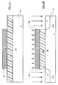
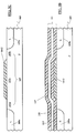
- FIGS. 1A to 1E are cross-sectional views showing the main steps of a fabrication process of a dual charge-storage location memory cell according to an embodiment of the present invention.
- a silicon dioxide (SiO 2 ) layer 101 is formed on a surface of a semiconductor layer 103, for example of the P conductivity type with a doping level ranging from 10 15 to 10 18 atoms/cm 3 .
- the silicon dioxide layer 101 is preferably rather thick, having for example a thickness of the order of 10 3 Angstroms.
- the silicon dioxide layer 101 can be formed by thermal oxidation or by chemical vapor deposition (CVD).
- the semiconductor layer 103 can be the substrate of a semiconductor wafer, or a doped semiconductor well formed in the wafer substrate.
- a photoresist layer 105 is deposited over the silicon dioxide layer 101 ; according to conventional photolithographic techniques, the photoresist layer 105 is exposed to a suitable radiation source (e . g ., UV rays) through a mask (not shown), then the photoresist layer is developed and selectively removed. A portion 1051 of the photoresist layer 105 is left on the silicon dioxide layer 101 over a region 107 of the semiconductor layer 103 intended to become a channel region of the memory cell.
- a suitable radiation source e . g ., UV rays
- the silicon dioxide layer 101 is then selectively removed from over the semiconductor layer 103 , by means of a selective etch process.
- the photoresist layer portion 1051 acts as an etch mask for the underlying silicon dioxide layer 101 , preventing it from being removed.
- a portion 1011 of the silicon dioxide layer 101 is thus left over the region 107 of the semiconductor layer 103 (FIG. 1B ).
- An N-type dopant is then introduced into the semiconductor layer 103 at the sides of the region 107 , so as to form source/drain regions 109a, 109b of the memory cells (FIG. 1B ).
- arsenic ions are implanted into the semiconductor layer 103 in a dose of the order of 10 15 atoms/cm 2 .
- the source/drain regions 109a, 109b result aligned with the edges of the silicon dioxide layer portion 1011.
- the photoresist layer 105 is then removed.
- the silicon dioxide layer portion 1011 is subjected to an isotropic etch, for example a wet etching, causing a substantial reduction of the thickness thereof.
- an isotropic etch for example a wet etching, causing a substantial reduction of the thickness thereof.
- a silicon dioxide film 1012 of, e.g. , 50 to 90 ⁇ is left over the semiconductor layer 103 .
- the etch rate is higher at the sides of the silicon dioxide layer portion 1011 than at the centre thereof, because the silicon dioxide layer portion 1011 is etched from more directions at the side than at the centre.
- the isotropic etch thus causes not only a thinning, but also a reduction of the lateral extension of the silicon dioxide layer portion 1011 , thereby the remaining silicon dioxide film 1012 is spaced apart from the source/drain regions 109a, 109b.
- Three sub-regions 107a , 107b and 107c can thus be identified in the semiconductor layer region 107 : two sub-regions 107a and 107b extend from the edge of the source/drain regions 109a and 109b, respectively, to the edge of the silicon dioxide film 1012 , and a sub-region 107c is located under the silicon dioxide film 1012 (FIG. 1C ).
- a stack 111 of three layers is then formed on the top surface of the structure.
- the stack of layers 111 comprises a bottom layer 113 of silicon dioxide, an intermediate layer 115 of silicon nitride and a top layer 117 of silicon dioxide.
- the oxide-nitride-oxide (ONO) stack of layers 111 can be formed by thermal growth or CVD, and has for example an overall thickness of 90 to 100 ⁇ .
- the nitride layer 115 will form the charge-storage element of the memory cell (FIG. 1D).
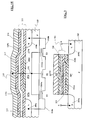
- a layer of polysilicon 119 is then formed over the ONO stack 111 (FIG. 1E ).
- the polysilicon layer 119 is preferably doped to increase the conductivity thereof.
- a layer of titanium or tungsten silicide is formed on the polysilicon layer, for further increasing the conductivity.
- the memory cell is functionally equivalent to three MOS transistors T1, T2, T3 connected in series between the two source/drain regions 109a , 109b .
- the lateral transistors T1 and T3 are each one adjacent a respective source/drain region 109a, 109b , and have each a control gate, formed by the polysilicon layer 119, and a charge-storage element, formed by a respective portion 115a, 115b of the nitride layer 111 above the semiconductor layer sub-region 107a, 107b with the interposition of the silicon dioxide layer 113 .
- Charges can be injected and become trapped into either one or both of the nitride layer portions 115a, 115b, thereby affecting the formation of an inversion layer in the respective underlying sub-region 107a , 107b of the semiconductor layer 103 .
- the central transistor T2 represented by the symbol of a normal MOSFET, has a gate formed by the polysilicon layer 119 and a gate dielectric formed by the superposition of the ONO stack 111 and the silicon dioxide film 1012.
- the memory cell thus have two source/drain electrodes S/Da, S/Db, formed by the source/drain regions 109a and 109b , a control gate CG formed by the polysilicon layer 119 , and two charge-storage elements CHSa and CHSb formed by the nitride layer portions 115a and 115b, respectively.
- the source/drain electrode S/Db opposite thereto acts as a memory cell source electrode in the programming phase of the transistor T1
- the source/drain electrode S/Da acts as a memory cell drain electrode, or programming electrode, in the programming phase of the transistor T1
- the control gate CG is raised to approximately 9 V. In this way, a current is made to flow from the source/drain electrode S/Da, while the control gate CG is raised to approximately 9 V. In this way, a current is made to flow from the source/drain electrode S/Da, while the control gate CG is raised to approximately 9 V. In this way, a current is made to flow from the source
- Electrons can be removed from the charge storage element CHSa by applying a sufficiently high positive voltage (e.g., 8 V) to the adjacent source/drain electrode S/Da, while keeping the control gate CG grounded and leaving the opposite source/drain electrode S/Db floating.
- a sufficiently high positive voltage e.g. 8 V
- the control gate CG is biased to a negative voltage (e . g ., -3 V) and the source/drain electrode S/Da is biased to a positive voltage (e.g., 5 V), while the opposite source/drain electrode S/Db is still left floating.
- the programming state of the left-hand lateral transistor T1 can be sensed by keeping the adjacent source/drain electrode S/Da (acting as the memory cell source electrode in the reading phase of the transistor T1 ) at the reference voltage, while applying positive voltages (lower than those used for programming, for example 1 or 2 V and 5 V, respectively) to the opposite source/drain electrode S/Db (acting as the memory cell drain electrode in reading the transistor T1) and to the control gate CG.
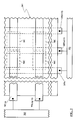
- FIG. 2 a portion of an array 201 of dual charge-storage location memory cells MC of the type described above is schematically depicted in top-plan view.
- the memory cells MC are conventionally arranged in rows and columns.
- the memory cells MC in each row have the respective control gates CG connected to a same word line, such as the two word lines WLm, WL(m+1) shown in the drawing.
- the word lines are polysilicon strips extending across the array in a first direction; referring back to FIG. 1E and assuming that this drawing is a cross-section of a memory cell MC of the array 201, the polysilicon layer 119 is an array word line in cross-section.
- the word lines are driven by a per-se known word line selector 203.
- the array 201 shown in FIG. 2 has the so-called contact-less structure, in which no electrical contacts to the source/drain regions of the memory cells are provided within the array.
- Elongated doped semiconductor regions 109n, 109(n+1), 109(n+2) extends across the array transversally to the word lines and forms array bit lines.
- the source/drain regions 109a, 109b of the memory cell are two array bit lines in cross-section. Outside the array 201, the bit lines 109n, 109(n+1), 109(n+2) are contacted by metal lines driven by a per-se known column selector 205.
- the memory cell according the above-described embodiment of the present invention can be used to build memory cell arrays of different structure, such as the traditional one with metal bit lines and contacts to the memory cells source/drain regions inside the array.
- the dielectric layer that separates the nitride layer 115 from the underlying semiconductor layer region 107 does not have a uniform thickness, and has instead different thickness in different sub-regions of the channel region.
- the thickness of the dielectric layer is lower over the lateral sub-regions 107a , 107b of the memory cell channel region 107 , near the source/drain regions 109a, 109b; the dielectric layer is thicker over the central sub-region 107c of the memory cell channel region 107 .
- This non-uniform thickness of the dielectric layer affects the vertical electric field along the memory cell's channel region.
- the vertical electric field along the memory cell channel region is kept rather low, except in the sub-region 107a or 107b under the nitride layer portion 115a or 115b (the memory cell's charge storage element CHSa or CHSb) into or from which electrons are to be injected or extracted.
- the injection and the extraction of electrons into and from either one of the two charge storage elements CHSa , CHSb are consequently strongly localised.
- the non-uniform thickness of the dielectric layer determines a vertical electric field distribution along the channel region that strongly disfavours the injection and trapping of electrons into the portion of the nitride layer 115 over the central sub-region 107c of the channel region 107, as well as any charge redistribution phenomenon.
- the charges injected into and trapped in the nitride layer 115 are therefore strongly localized at the nitride layer portions 115a, 115b, adjacent the memory cell source/drain regions 109a, 109b, where they can be relatively easily removed during the erase operation.
- the memory cell according to the above-described embodiment of the present invention is thus not subjected to a fast aging caused by the presence of charges trapped in central portion of the nitride layer, where they can hardly be removed.
- the memory cell can withstand a high number of program/erase cycles.
- the distributions of threshold voltage values are rather narrow: a lower threshold voltage shift is thus sufficient to guarantee the discrimination between an erased and a written bit. Thanks to this, small amount of charges need to be injected to achieve the desired threshold voltage shift, which reduces the memory cell aging.
- the strong localisation of the charges in the two charge-storage elements strongly reduces the influence of the charges injected into one charge-storage element on the other one.
- the memory cell operating area in terms of threshold voltage values, is consequently increased. In conjunction with the fact that even a small threshold voltage shift can be discriminated, this allows allocating more than two threshold voltage levels, thus making it possible to implement multi-level approaches.
- a thinner dielectric layer near the source/drain regions also allows reducing the current that needs to be made to flow through the memory cell in the programming phase.
- a rather high current is normally needed to produce channel hot electrons of sufficiently high energy, capable of overcoming the potential barrier between the channel region and the charge storage elements.
- a lower dielectric thickness reduces the electric potential barrier that the electrons need to overcome to be injected into the charge storage elements; consequently, channel hot electrons of lower energy can overcome said potential barrier.
- a reduced programming current allows increasing the degree of parallelism of the memory in programming, and thus reduces the programming time.
- FIG. 3 shows in a simplified cross-sectional view an electrically-programmable memory cell according to another embodiment of the present invention.
- the memory cell comprises N-type source 309a and drain 309b regions formed in a P-type semiconductor layer 303 .
- the source and drain regions 309a and 309b respectively forming a source electrode S and a drain electrode D , are spaced apart and define a channel region 307 there between.
- a dielectric layer 321 is placed over the channel region 307 .
- the dielectric layer 321 for example of silicon dioxide, comprises a first portion 321a and a second portion 321b , the second portion 321b being adjacent the drain region 309b and having a lower thickness than the first portion 321a .
- a conductive layer 323 for example of polysilicon, is placed over the dielectric layer 321 .
- the conductive layer 323 forms a floating gate, and is separated by an overlying conductive layer 319 forming a control gate CG by an ONO stack 311 .
- the memory cell of FIG. 3 is programmed by applying sufficiently high positive potentials to the control gate CG and to the drain D (acting as a programming electrode), while keeping the source grounded.
- the provision of the dielectric portion 321b of reduced thickness near the drain electrode facilitates injection of channel hot electrons into the floating gate, thereby allowing to reduce the programming current.
- the programming current is also expected to be further reduced due to the contribution of an electron tunnelling mechanism, consequence of the reduced thickness of the dielectric portion 321b .
- the memory cell of FIG. 3 can be fabricated by a process providing for a selectively etching the dielectric layer 321 to reduce the thickness thereof in the portion 321b .
- the dielectric layer 321 may also include a second portion of reduced thickness near the source region 309a. This allows extracting charges from the floating gate by means of a Fowler-Nordheim tunnelling mechanism at the memory cell source S.
- This memory cell can be fabricated by a process similar to the one previously described.
- the fabrication process previously described merely exemplifies an embodiment, albeit preferred, of the invention.
- Alternative ways of forming a silicon dioxide layer having differentiated thickness can be envisaged.
- a selective silicon dioxide growth over the central portion 107c of the channel regions can be carried out.
- the process previously described allows forming a symmetric structure.
- the silicon nitride layer may be substituted for by a different charge-trapping dielectric material.
- the silicon dioxide layers forming the bottom and top layers of the ONO stack of layers may be substituted for by different dielectrics, particularly high-k ( i . e ., high dielectric constant) dielectrics such as the promising ZrO 2 and HfO 2 .
- the present invention can be applied in general to the fabrication of any type of electrically modifiable non-volatile memory programmable by hot-electron injection, such as the EPROMs and the Flash EPROMs.
Landscapes
- Engineering & Computer Science (AREA)
- Microelectronics & Electronic Packaging (AREA)
- Computer Hardware Design (AREA)
- Non-Volatile Memory (AREA)
- Semiconductor Memories (AREA)
Abstract
Description
Summarising, the process comprises:
Claims (13)
- An electrically-programmable memory cell programmed by means of injection of channel hot electrons into a charge-storage element (115a,115b;323) capacitively coupled to a memory cell channel (107;307) for modulating a conductivity thereof depending on a stored amount of charge, comprising:characterised in thata first and a second spaced-apart electrode regions (109a,109b;309a,309b) formed in a semiconductor layer (103;303) and defining a channel region (107;307) there between, at least one (109A,109B;309B) of the first and second electrode regions acting as a programming electrode of the memory cell;a control electrode (CG) capacitively coupled to the charge-storage element,the charge-storage element being placed over the channel to substantially extend from the first to the second electrode regions, and being separated from the channel region by a dielectric layer (1012,113;321),the dielectric layer has a reduced thickness in a portion (113;321b) thereof near the at least one programming electrode.
- The memory cell according to claim 1, in which the charge-storage element comprises a charge-trapping layer (115) having a first and a second charge-storage locations (115a,115b) near the first and second electrode regions, respectively, the first and second electrode regions alternatively acting as programming electrodes,the dielectric layer having a lower thickness near the first and second electrode regions and a greater thickness over a central portion (107c) of the channel region.
- The memory cell according to claim 2, in which the dielectric layer comprises a first dielectric layer (1012) placed over the central portion of the channel region, and a second dielectric layer (113) placed over the whole channel region, the second dielectric layer being superimposed on the first dielectric layer over the central portion of the channel region.
- The memory cell according to claim 3, in which the first dielectric layer is a layer of silicon dioxide.
- The memory cell according to claim 3 or 4, in which the second dielectric layer is a layer of silicon dioxide.
- The memory cell according to any one of the preceding claims, in which the charge-trapping layer is a layer of silicon nitride.
- The memory cell according to claim 1, in which the charge-storage element is a conductive layer, particularly a polysilicon layer.
- A process for fabricating an electrically-programmable memory cell programmed by means of injection of channel hot electrons into a charge-storage element (115a,115b;323) capacitively coupled to a memory cell channel (107;307) for modulating a conductivity thereof depending on a stored amount of charge, comprising:characterised by comprisingforming a first and a second spaced-apart electrode regions (109a,109b;309a,309b) in a semiconductor layer (103;303), the first and second electrode regions defining a channel region (107;307) there between, at least one (109a,109b;309b) of the first and second electrode regions designed to act as a programming electrode of the memory cell;placing a charge-storage layer (115;323) over the channel region with interposition of a dielectric layer (1012,113;321), the charge-storage layer substantially extending from the first to the second electrode regions;forming a control electrode (CG) capacitively coupled to the charge-storage layer,forming the dielectric layer with a reduced thickness (113;321b) in a portion thereof near the at least one programming electrode.
- The process according to claim 8, comprising:placing a charge-trapping layer (115) over the channel region (107) with interposition of the dielectric layer (111,1012);forming the dielectric layer with a lower thickness (113) near the first and second electrode regions (109a,109b) and a greater thickness over a central portion (107c) of the channel region.
- The process according to claim 9, in which said forming the dielectric layer comprises:forming a first dielectric layer (113) over the whole channel region;selectively forming a second dielectric layer (1012) only over the central portion (107c) of the channel region.
- The process according to claim 10, in which said selectively forming the second dielectric layer comprises:forming a thick dielectric layer (1011) over the whole channel region, the thick dielectric layer having a thickness greater than the second dielectric layer;isotropically etching the thick dielectric layer to reduce the thickness of the thick dielectric layer to a prescribed thickness and remove the thick dielectric layer from over lateral portions (107a,107b) of the channel region between the first and second electrode regions and the central channel portion.
- The process according to claim 11, in which said forming the first and second electrode regions comprises introducing dopants into the semiconductor layer in alignment with the thick dielectric layer.
- The process according to any one of claims 8 to 12, in which the dielectric layer is made of silicon dioxide, and the charge-trapping layer is a layer of silicon nitride.
Priority Applications (3)
| Application Number | Priority Date | Filing Date | Title |
|---|---|---|---|
| DE60226571T DE60226571D1 (en) | 2002-02-20 | 2002-02-20 | Electrically programmable non-volatile memory cell |
| EP02425085A EP1339068B1 (en) | 2002-02-20 | 2002-02-20 | Electrically programmable non-volatile memory cell |
| US10/372,044 US6882001B2 (en) | 2002-02-20 | 2003-02-20 | Electrically-programmable non-volatile memory cell |
Applications Claiming Priority (1)
| Application Number | Priority Date | Filing Date | Title |
|---|---|---|---|
| EP02425085A EP1339068B1 (en) | 2002-02-20 | 2002-02-20 | Electrically programmable non-volatile memory cell |
Publications (2)
| Publication Number | Publication Date |
|---|---|
| EP1339068A1 true EP1339068A1 (en) | 2003-08-27 |
| EP1339068B1 EP1339068B1 (en) | 2008-05-14 |
Family
ID=27635927
Family Applications (1)
| Application Number | Title | Priority Date | Filing Date |
|---|---|---|---|
| EP02425085A Expired - Lifetime EP1339068B1 (en) | 2002-02-20 | 2002-02-20 | Electrically programmable non-volatile memory cell |
Country Status (3)
| Country | Link |
|---|---|
| US (1) | US6882001B2 (en) |
| EP (1) | EP1339068B1 (en) |
| DE (1) | DE60226571D1 (en) |
Cited By (1)
| Publication number | Priority date | Publication date | Assignee | Title |
|---|---|---|---|---|
| EP1717815A1 (en) * | 2005-04-29 | 2006-11-02 | Macronix International Co., Ltd. | Inversion bit line, charge trapping non-volatile memory and method of operating same |
Families Citing this family (2)
| Publication number | Priority date | Publication date | Assignee | Title |
|---|---|---|---|---|
| US7388252B2 (en) * | 2005-09-23 | 2008-06-17 | Macronix International Co., Ltd. | Two-bits per cell not-and-gate (NAND) nitride trap memory |
| US8139418B2 (en) * | 2009-04-27 | 2012-03-20 | Micron Technology, Inc. | Techniques for controlling a direct injection semiconductor memory device |
Citations (4)
| Publication number | Priority date | Publication date | Assignee | Title |
|---|---|---|---|---|
| US4586065A (en) * | 1982-02-25 | 1986-04-29 | U.S. Philips Corporation | MNOS memory cell without sidewalk |
| EP0778581A2 (en) * | 1995-12-07 | 1997-06-11 | Samsung Electronics Co., Ltd. | Nonvolatile memory device |
| US5739568A (en) * | 1994-11-28 | 1998-04-14 | Motorola, Inc. | Non-volatile memory having a cell applying to multi-bit data by double layered floating gate architecture and programming method for the same |
| US6243300B1 (en) * | 2000-02-16 | 2001-06-05 | Advanced Micro Devices, Inc. | Substrate hole injection for neutralizing spillover charge generated during programming of a non-volatile memory cell |
Family Cites Families (9)
| Publication number | Priority date | Publication date | Assignee | Title |
|---|---|---|---|---|
| JPH021988A (en) * | 1987-12-03 | 1990-01-08 | Texas Instr Inc <Ti> | Electrically programmable memory cell |
| US5156991A (en) * | 1988-02-05 | 1992-10-20 | Texas Instruments Incorporated | Fabricating an electrically-erasable, electrically-programmable read-only memory having a tunnel window insulator and thick oxide isolation between wordlines |
| US5444279A (en) * | 1993-08-11 | 1995-08-22 | Micron Semiconductor, Inc. | Floating gate memory device having discontinuous gate oxide thickness over the channel region |
| WO1996013863A2 (en) * | 1994-10-28 | 1996-05-09 | Philips Electronics N.V. | Field effect device |
| US5844271A (en) * | 1995-08-21 | 1998-12-01 | Cypress Semiconductor Corp. | Single layer polycrystalline silicon split-gate EEPROM cell having a buried control gate |
| TW332344B (en) * | 1997-02-27 | 1998-05-21 | Philips Electronics Nv | Semiconductor device with a programmable semiconductor element |
| US5889700A (en) * | 1997-05-05 | 1999-03-30 | National Semiconductor Corporation | High density EEPROM array using self-aligned control gate and floating gate for both access transistor and memory cell and method of operating same |
| US6242773B1 (en) * | 1998-09-30 | 2001-06-05 | Advanced Micro Devices, Inc. | Self-aligning poly 1 ono dielectric for non-volatile memory |
| US6734491B1 (en) * | 2002-12-30 | 2004-05-11 | Texas Instruments Deutschland Gmbh | EEPROM with reduced manufacturing complexity |
-
2002
- 2002-02-20 EP EP02425085A patent/EP1339068B1/en not_active Expired - Lifetime
- 2002-02-20 DE DE60226571T patent/DE60226571D1/en not_active Expired - Lifetime
-
2003
- 2003-02-20 US US10/372,044 patent/US6882001B2/en not_active Expired - Fee Related
Patent Citations (4)
| Publication number | Priority date | Publication date | Assignee | Title |
|---|---|---|---|---|
| US4586065A (en) * | 1982-02-25 | 1986-04-29 | U.S. Philips Corporation | MNOS memory cell without sidewalk |
| US5739568A (en) * | 1994-11-28 | 1998-04-14 | Motorola, Inc. | Non-volatile memory having a cell applying to multi-bit data by double layered floating gate architecture and programming method for the same |
| EP0778581A2 (en) * | 1995-12-07 | 1997-06-11 | Samsung Electronics Co., Ltd. | Nonvolatile memory device |
| US6243300B1 (en) * | 2000-02-16 | 2001-06-05 | Advanced Micro Devices, Inc. | Substrate hole injection for neutralizing spillover charge generated during programming of a non-volatile memory cell |
Cited By (1)
| Publication number | Priority date | Publication date | Assignee | Title |
|---|---|---|---|---|
| EP1717815A1 (en) * | 2005-04-29 | 2006-11-02 | Macronix International Co., Ltd. | Inversion bit line, charge trapping non-volatile memory and method of operating same |
Also Published As
| Publication number | Publication date |
|---|---|
| US20030197217A1 (en) | 2003-10-23 |
| US6882001B2 (en) | 2005-04-19 |
| EP1339068B1 (en) | 2008-05-14 |
| DE60226571D1 (en) | 2008-06-26 |
Similar Documents
| Publication | Publication Date | Title |
|---|---|---|
| US6784476B2 (en) | Semiconductor device having a flash memory cell and fabrication method thereof | |
| US7115472B2 (en) | Process for manufacturing a dual charge storage location memory cell | |
| US5494838A (en) | Process of making EEPROM memory device having a sidewall spacer floating gate electrode | |
| US6844588B2 (en) | Non-volatile memory | |
| US9847343B2 (en) | Charge trapping nonvolatile memory devices, methods of fabricating the same, and methods of operating the same | |
| US7382662B2 (en) | Twin insulator charge storage device operation and its fabrication method | |
| KR20030024878A (en) | Non-volatile memory, method of manufacture and programming | |
| KR20020033792A (en) | Semiconductor non-volatile memory device | |
| US10217759B2 (en) | Semiconductor device | |
| KR20060021054A (en) | Nonvolatile memory device, method for manufacturing same and method for operating same | |
| US7411247B2 (en) | Twin insulator charge storage device operation and its fabrication method | |
| JP2004214365A (en) | Nonvolatile semiconductor memory device and method of operating the same | |
| US6958510B2 (en) | Process for fabricating a dual charge storage location memory cell | |
| US6987048B1 (en) | Memory device having silicided bitlines and method of forming the same | |
| US20060180847A1 (en) | Two-bit non-volatile memory devices including independently-controllable gate electrodes and methods for fabricating the same | |
| US7391653B2 (en) | Twin insulator charge storage device operation and its fabrication method | |
| EP1339068B1 (en) | Electrically programmable non-volatile memory cell | |
| US6839278B1 (en) | Highly-integrated flash memory and mask ROM array architecture |
Legal Events
| Date | Code | Title | Description |
|---|---|---|---|
| PUAI | Public reference made under article 153(3) epc to a published international application that has entered the european phase |
Free format text: ORIGINAL CODE: 0009012 |
|
| AK | Designated contracting states |
Designated state(s): AT BE CH CY DE DK ES FI FR GB GR IE IT LI LU MC NL PT SE TR |
|
| AX | Request for extension of the european patent |
Extension state: AL LT LV MK RO SI |
|
| 17P | Request for examination filed |
Effective date: 20030822 |
|
| 17Q | First examination report despatched |
Effective date: 20030930 |
|
| AKX | Designation fees paid |
Designated state(s): DE FR GB IT |
|
| GRAP | Despatch of communication of intention to grant a patent |
Free format text: ORIGINAL CODE: EPIDOSNIGR1 |
|
| GRAS | Grant fee paid |
Free format text: ORIGINAL CODE: EPIDOSNIGR3 |
|
| GRAA | (expected) grant |
Free format text: ORIGINAL CODE: 0009210 |
|
| AK | Designated contracting states |
Kind code of ref document: B1 Designated state(s): DE FR GB IT |
|
| REG | Reference to a national code |
Ref country code: GB Ref legal event code: FG4D |
|
| REF | Corresponds to: |
Ref document number: 60226571 Country of ref document: DE Date of ref document: 20080626 Kind code of ref document: P |
|
| PLBE | No opposition filed within time limit |
Free format text: ORIGINAL CODE: 0009261 |
|
| STAA | Information on the status of an ep patent application or granted ep patent |
Free format text: STATUS: NO OPPOSITION FILED WITHIN TIME LIMIT |
|
| 26N | No opposition filed |
Effective date: 20090217 |
|
| PGFP | Annual fee paid to national office [announced via postgrant information from national office to epo] |
Ref country code: GB Payment date: 20090128 Year of fee payment: 8 |
|
| PG25 | Lapsed in a contracting state [announced via postgrant information from national office to epo] |
Ref country code: IT Free format text: LAPSE BECAUSE OF FAILURE TO SUBMIT A TRANSLATION OF THE DESCRIPTION OR TO PAY THE FEE WITHIN THE PRESCRIBED TIME-LIMIT Effective date: 20080514 |
|
| REG | Reference to a national code |
Ref country code: FR Ref legal event code: ST Effective date: 20091030 |
|
| PG25 | Lapsed in a contracting state [announced via postgrant information from national office to epo] |
Ref country code: FR Free format text: LAPSE BECAUSE OF NON-PAYMENT OF DUE FEES Effective date: 20090302 |
|
| GBPC | Gb: european patent ceased through non-payment of renewal fee |
Effective date: 20100220 |
|
| PG25 | Lapsed in a contracting state [announced via postgrant information from national office to epo] |
Ref country code: GB Free format text: LAPSE BECAUSE OF NON-PAYMENT OF DUE FEES Effective date: 20100220 |
|
| PGFP | Annual fee paid to national office [announced via postgrant information from national office to epo] |
Ref country code: DE Payment date: 20120215 Year of fee payment: 11 |
|
| REG | Reference to a national code |
Ref country code: DE Ref legal event code: R119 Ref document number: 60226571 Country of ref document: DE Effective date: 20130903 |
|
| PG25 | Lapsed in a contracting state [announced via postgrant information from national office to epo] |
Ref country code: DE Free format text: LAPSE BECAUSE OF NON-PAYMENT OF DUE FEES Effective date: 20130903 |