EP1339059A2 - Method of producing master information carrier for magnetic transfer - Google Patents
Method of producing master information carrier for magnetic transfer Download PDFInfo
- Publication number
- EP1339059A2 EP1339059A2 EP03004212A EP03004212A EP1339059A2 EP 1339059 A2 EP1339059 A2 EP 1339059A2 EP 03004212 A EP03004212 A EP 03004212A EP 03004212 A EP03004212 A EP 03004212A EP 1339059 A2 EP1339059 A2 EP 1339059A2
- Authority
- EP
- European Patent Office
- Prior art keywords
- electron beam
- substrate
- master information
- information carrier
- pattern
- Prior art date
- Legal status (The legal status is an assumption and is not a legal conclusion. Google has not performed a legal analysis and makes no representation as to the accuracy of the status listed.)
- Withdrawn
Links
- 238000000034 method Methods 0.000 title claims description 29
- 239000000758 substrate Substances 0.000 claims abstract description 54
- 238000010894 electron beam technology Methods 0.000 claims abstract description 53
- 239000011295 pitch Substances 0.000 claims description 2
- 239000002184 metal Substances 0.000 description 14
- 229910052751 metal Inorganic materials 0.000 description 14
- 239000011347 resin Substances 0.000 description 10
- 229920005989 resin Polymers 0.000 description 10
- 230000005415 magnetization Effects 0.000 description 7
- 239000000696 magnetic material Substances 0.000 description 4
- 239000000463 material Substances 0.000 description 4
- 238000007747 plating Methods 0.000 description 4
- 229910002546 FeCo Inorganic materials 0.000 description 3
- 229910002545 FeCoNi Inorganic materials 0.000 description 3
- 239000011521 glass Substances 0.000 description 3
- 238000004528 spin coating Methods 0.000 description 3
- 229910000531 Co alloy Inorganic materials 0.000 description 2
- 229910002441 CoNi Inorganic materials 0.000 description 2
- 229910000684 Cobalt-chrome Inorganic materials 0.000 description 2
- 229910000640 Fe alloy Inorganic materials 0.000 description 2
- 229910000990 Ni alloy Inorganic materials 0.000 description 2
- 239000000969 carrier Substances 0.000 description 2
- 239000011248 coating agent Substances 0.000 description 2
- 238000000576 coating method Methods 0.000 description 2
- 239000010952 cobalt-chrome Substances 0.000 description 2
- 238000001723 curing Methods 0.000 description 2
- 238000005323 electroforming Methods 0.000 description 2
- 238000007733 ion plating Methods 0.000 description 2
- 229920000515 polycarbonate Polymers 0.000 description 2
- 239000004417 polycarbonate Substances 0.000 description 2
- 239000010453 quartz Substances 0.000 description 2
- VYPSYNLAJGMNEJ-UHFFFAOYSA-N silicon dioxide Inorganic materials O=[Si]=O VYPSYNLAJGMNEJ-UHFFFAOYSA-N 0.000 description 2
- 238000004544 sputter deposition Methods 0.000 description 2
- 239000006188 syrup Substances 0.000 description 2
- 235000020357 syrup Nutrition 0.000 description 2
- 229910001149 41xx steel Inorganic materials 0.000 description 1
- 239000004925 Acrylic resin Substances 0.000 description 1
- 229920000178 Acrylic resin Polymers 0.000 description 1
- -1 CoPtCr Inorganic materials 0.000 description 1
- 229910015372 FeAl Inorganic materials 0.000 description 1
- 229910005335 FePt Inorganic materials 0.000 description 1
- 229910005435 FeTaN Inorganic materials 0.000 description 1
- 229910001030 Iron–nickel alloy Inorganic materials 0.000 description 1
- 229910000943 NiAl Inorganic materials 0.000 description 1
- NPXOKRUENSOPAO-UHFFFAOYSA-N Raney nickel Chemical compound [Al].[Ni] NPXOKRUENSOPAO-UHFFFAOYSA-N 0.000 description 1
- BZHJMEDXRYGGRV-UHFFFAOYSA-N Vinyl chloride Chemical compound ClC=C BZHJMEDXRYGGRV-UHFFFAOYSA-N 0.000 description 1
- 229920001577 copolymer Polymers 0.000 description 1
- 230000003247 decreasing effect Effects 0.000 description 1
- 238000007772 electroless plating Methods 0.000 description 1
- 238000001227 electron beam curing Methods 0.000 description 1
- 239000003822 epoxy resin Substances 0.000 description 1
- 238000005530 etching Methods 0.000 description 1
- 230000004907 flux Effects 0.000 description 1
- LNEPOXFFQSENCJ-UHFFFAOYSA-N haloperidol Chemical compound C1CC(O)(C=2C=CC(Cl)=CC=2)CCN1CCCC(=O)C1=CC=C(F)C=C1 LNEPOXFFQSENCJ-UHFFFAOYSA-N 0.000 description 1
- 238000004519 manufacturing process Methods 0.000 description 1
- 239000003960 organic solvent Substances 0.000 description 1
- 230000035699 permeability Effects 0.000 description 1
- 238000005498 polishing Methods 0.000 description 1
- 229920003229 poly(methyl methacrylate) Polymers 0.000 description 1
- 229920000647 polyepoxide Polymers 0.000 description 1
- 229920000728 polyester Polymers 0.000 description 1
- 239000004926 polymethyl methacrylate Substances 0.000 description 1
- 229920000098 polyolefin Polymers 0.000 description 1
- 239000004800 polyvinyl chloride Substances 0.000 description 1
- 229920000915 polyvinyl chloride Polymers 0.000 description 1
- 238000003825 pressing Methods 0.000 description 1
- 230000035945 sensitivity Effects 0.000 description 1
- 229910052710 silicon Inorganic materials 0.000 description 1
- 239000010703 silicon Substances 0.000 description 1
- 238000004804 winding Methods 0.000 description 1
Images


Classifications
-
- G—PHYSICS
- G11—INFORMATION STORAGE
- G11B—INFORMATION STORAGE BASED ON RELATIVE MOVEMENT BETWEEN RECORD CARRIER AND TRANSDUCER
- G11B5/00—Recording by magnetisation or demagnetisation of a record carrier; Reproducing by magnetic means; Record carriers therefor
- G11B5/48—Disposition or mounting of heads or head supports relative to record carriers ; arrangements of heads, e.g. for scanning the record carrier to increase the relative speed
- G11B5/58—Disposition or mounting of heads or head supports relative to record carriers ; arrangements of heads, e.g. for scanning the record carrier to increase the relative speed with provision for moving the head for the purpose of maintaining alignment of the head relative to the record carrier during transducing operation, e.g. to compensate for surface irregularities of the latter or for track following
- G11B5/596—Disposition or mounting of heads or head supports relative to record carriers ; arrangements of heads, e.g. for scanning the record carrier to increase the relative speed with provision for moving the head for the purpose of maintaining alignment of the head relative to the record carrier during transducing operation, e.g. to compensate for surface irregularities of the latter or for track following for track following on disks
- G11B5/59633—Servo formatting
-
- G—PHYSICS
- G11—INFORMATION STORAGE
- G11B—INFORMATION STORAGE BASED ON RELATIVE MOVEMENT BETWEEN RECORD CARRIER AND TRANSDUCER
- G11B5/00—Recording by magnetisation or demagnetisation of a record carrier; Reproducing by magnetic means; Record carriers therefor
- G11B5/86—Re-recording, i.e. transcribing information from one magnetisable record carrier on to one or more similar or dissimilar record carriers
-
- G—PHYSICS
- G11—INFORMATION STORAGE
- G11B—INFORMATION STORAGE BASED ON RELATIVE MOVEMENT BETWEEN RECORD CARRIER AND TRANSDUCER
- G11B5/00—Recording by magnetisation or demagnetisation of a record carrier; Reproducing by magnetic means; Record carriers therefor
- G11B5/74—Record carriers characterised by the form, e.g. sheet shaped to wrap around a drum
- G11B5/82—Disk carriers
Definitions
- This invention relates to a method of producing a master information carrier for magnetic transfer provided with an irregularity pattern (a pattern of protruding portions and recessed portions) representing information to be transferred to a magnetic recording medium, and more particularly to a method of producing an original for duplicating such master information carriers where the irregularity pattern is a phase servo pattern at an angle to the recording tracks and the phase servo pattern is drawn with an electron beam.
- an irregularity pattern a pattern of protruding portions and recessed portions
- areas for recording servo information including, for instance, a servo signal for locating a recording track, an address signal representing the address of the recording track and a reproduction clock signal are provided at predetermined angular intervals.
- a method of recording a servo signal on the magnetic recording medium magnetic transfer has been wide used.
- the surface of a master information carrier having thereon an irregularity pattern (a pattern of protruding portions and recessed portions) of magnetic material representing information to be transferred is brought into close contact with a surface of a magnetic recording medium (a slave medium) having a magnetic layer and a transfer magnetic field is applied to the slave medium and the master information carrier in this state, thereby recording on the slave medium a magnetization pattern representing the information (e.g., a servo signal) on the master information carrier.
- the master information carrier is produced on the basis of an original carrying thereon an irregularity pattern of resist (servo pattern) representing the information to be recorded on the slave medium.
- the irregularity pattern is formed by uniformly coating resist on a disc-like substrate of, for instance, glass, for instance, by spin coating, projecting onto the resist a laser beam or an electron beam modulated according to the information to be recorded on the slave medium, and developing the resist.
- a laser beam prevails over use of an electron beam at present, as the track width and the pattern width are narrowed to meet demand for a higher recording density, a laser beam will become too large in beam diameter.
- This problem may be overcome by drawing the irregularity pattern on the resist by an electron beam having a smaller beam diameter than a laser beam by turning on and off the electron beam while rotating the substrate and exposing each element of the pattern at one time or more times.
- this approach is disadvantageous in that it is difficult to accurately locate the fine electron beam spot in the next position and to accurately control the exposing time for the pattern width of a sub-micron order, which causes non-uniformity in exposure in one element and makes it impossible to form a clear pattern.
- the primary object of the present invention is to provide a method of accurately drawing a phase servo pattern at an angle to the recording tracks with an electron beam.
- a method of producing a master information carrier from an original on which a phase servo pattern is drawn by scanning the original with an electron beam wherein the improvement comprises that the phase servo pattern is drawn element by element by causing the electron beam having a beam diameter not larger than the minimum width of the element to scan a disc-like substrate of the original, which has been provided with a resist layer for electron beam drawing, in a diametrical direction of the disc-like substrate while rotating the substrate in one direction at a constant speed.
- a diametrical direction of the disc-like substrate should be broadly interpreted here to include, as well as a diametrical direction of the disc-like substrate in the strict sense of the word, directions where the angle ⁇ (°) between the direction and a radial direction is 0 ⁇ 90.
- an oblique side of an element is zigzagged and the pattern cannot be excellent in shape.
- an element of the pattern is continuously drawn by an electron beam whose beam diameter is equal to the width of the element.
- an oblique side of the element can be substantially linear and the pattern can be excellent in shape.
- an electron beam whose beam diameter is smaller than the width of the element is caused to scan at fine pitches to completely cover an element. In this case, each element is uniformly covered with the electron beam and non-uniformity in exposure in one element is not caused, whereby an excellent pattern can be obtained.
- the electron gun since the electron gun has only to be one-dimensionally controlled, the electron gun can be accurately controlled and an excellent pattern high in reproducibility can be formed.
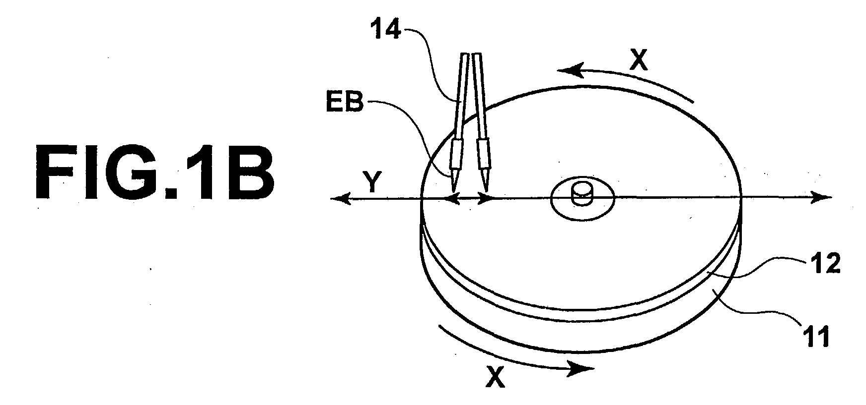
- Figures 1A to 1C are views for illustrating steps of producing an original from which a master information carrier is duplicated.
- a resist solution 12' comprising a positive-type electron beam drawing resist 12 dissolved in an organic solvent, is applied to a disc-like substrate 11 of glass or quartz by spin coating from a nozzle 13 while rotating the disc-like substrate 11 in one direction and then the substrate 11 is baked.
- an electron beam EB modulated according to a servo signal is caused to finely scan the disc-like substrate 11, carrying thereon the resist 12, in a direction of arrow Y (a diametrical direction of the disc-like substrate 11) while rotating the substrate in the direction of arrow X, to expose an area corresponding to the servo signal element by element.
- the electron beam EB is converged to a beam diameter not larger than the minimum width of the element by a known electron gun 14.
- the positive electron beam drawing resist 12 is developed and a substrate 11 on which the phase servo pattern 15 to be transferred is recorded is obtained.
- This substrate 11 is an original from which a master information carrier is duplicated.
- the phase servo pattern 15 thus recorded comprises a plurality of elements 12a at an angle of ⁇ to a diametrical direction of the substrate 11 (the direction of arrow Y) . That is, the resist 12 is removed from the areas exposed to the electron beam (hatched portions in Figure 2) upon development of the resist 12 with protrusions of the resist 12 left at predetermined intervals.
- a positive-type electron beam drawing resist is employed in this particular embodiment, a negative-type electron beam drawing resist can also be employed.
- the disc-like substrate 11 may be formed, for instance, of, silicon, glass or quartz.
- the servo pattern shown in Figure 3 comprises a plurality of elements 12a which are (1 long and are at an angle of ⁇ 1 to a diametrical direction of the substrate 11 (the direction of arrow Y) .
- the elements 12a are drawn, for instance, by swinging an electron gun 14 emitting an electron beam EB having a beam diameter d equal to the width of the element 12a so that the electron beam EB scans positive electron beam drawing resist 12 on a disc-like substrate 11 in a diametrical direction of the substrate 11 from Y1 to Y2 while rotating the substrate 11 in the direction of arrow X. That is, the electron beam EB first obliquely scans the resist 12 from point Y11 to point Y21 to draw the leftmost element 12a. When the electron beam EB reaches the point Y21, the electron gun 14 is turned off and returned to Y1. Since the substrate 11 is rotated, the electron gun 14 is obliquely brought to point Y12. Then the electron gun 14 is turned on again and the electron beam EB is caused to scan from Y1 to Y2 (Y12 to Y22), whereby the second leftmost element 12a is drawn. In the similar manner, the other elements are drawn.
- the servo pattern shown in Figure 4 comprises a plurality of elements 12a which are l2 long and are at an angle of ⁇ 2 to a diametrical direction of the substrate 11 (the direction of arrow Y) .
- the elements 12a are drawn, for instance, by swinging an electron gun 14 emitting an electron beam EB having a beam diameter d equal to the width of the element 12a so that the electron beam EB scans positive electron beam drawing resist 12 on a disc-like substrate 11 in a diametrical direction of the substrate 11 from Y1 to Y2 while rotating the substrate 11 in the direction of arrow X. That is, the electron beam EB first obliquely scans the resist 12 from point Y11 to point Y21 to draw the leftmost element 12a. When the electron beam EB reaches the point Y21, the electron gun 14 is turned off and returned to Y1.
- the electron gun 14 cannot be returned to the starting point Y12 of the second leftmost element 12a due to the swinging speed of the electron gun 14 with respect to the rotating speed of the substrate 11.
- elements which cannot be drawn from their starting points are not drawn in the first rotation of the substrate 11, and are drawn in the second or following other rotation of the substrate 11. Then elements which can be drawn from their starting points are only drawn in the first rotation of the substrate 11. That is, the substrate 11 is kept rotated until all the elements in one recording track are drawn.
- phase servo pattern can be drawn easily in a short time since the pattern is drawn by an electron beam whose beam diameter is equal to the width of the element but are disadvantageous in that the edges are rounded since it is impossible to expose the resist up to just edges of the pattern.
- the servo pattern shown in Figure 5 comprises a plurality of elements 12a which are l3 long and are at an angle of ⁇ 3 to a diametrical direction of the substrate 11 (the direction of arrow Y).
- the elements 12a are drawn, for instance, by repeatedly swinging an electron gun 14 emitting an electron beam EB having a beam diameter sufficiently smaller than the width of the element 12a while moving the gun 14 from Y1 to Y2 and rotating the substrate 11 in the direction of arrow X so that the electron beam EB scans positive electron beam drawing resist 12 on a disc-like substrate 11 in a diametrical direction of the substrate 11 by an increasing distance as the electron gun 14 moves away from Y1 to a predetermined distance therefrom, by a constant distance as the electron gun 14 moves from the predetermined distance from Y1 to a predetermined distance from Y2 and by a decreasing distance as the electron gun 14 moves from the predetermined distance from Y2 to Y2.
- the electron gun 14 When the electron beam EB reaches the point Y21, the electron gun 14 is turned off and returned to Y1. Since the substrate 11 is rotated, the electron gun 14 is obliquely brought to point Y12. Then the electron gun 14 is turned on again and the electron beam EB is caused to scan from Y1 to Y2 (Y12 to Y22), whereby the second leftmost element 12a is drawn. In the similar manner, the other elements are drawn.
- the electron beam output and the beam diameter be adjusted taking into account the shape of the phase servo pattern and the sensitivity of the electron beam drawing resist.
- phase servo pattern need not be limited to those accommodated within one track width but even those extending from one track to other one or more tracks may be drawn in a similar manner.
- a phase servo pattern is drawn on a positive-type electron beam drawing resist 12 by projecting an electron beam EB in the manner described above and the resist 12 in the area 12a exposed to the electron beam EB is removed by developing the resist, whereby an original carrying thereon a servo pattern of the resist 12 is obtained.
- the metal disc 31 may be used as a master information carrier, or the metal disc 31 provided with a soft magnetic layer 32 on the surface of irregularity pattern as shown in Figure 6D may be used as a master information carrier.
- the original may be plated to form a second original and the second original may be plated to form a metal disc having a negative irregularity pattern.
- a third original may be formed by plating the second original or pressing a resin syrup against the surface of the second original and curing the resin syrup, and a metal disc having a positive irregularity pattern may be formed by plating the third original.
- the disc-like substrate 11 selectively covered with the resist 12 left thereon may be etched and an original may be obtained by removing the resist 12 after etching. Thereafter, a metal disc 31 can be obtained from the original in the same manner as described above.
- the metal disc 31 may be formed of Ni or Ni alloys.
- the metal disc 31 may be formed by plating such as various metal film forming techniques including electroless plating, electroforming, sputtering, and ion plating.
- the depth of the irregularity pattern (the height of the protrusions) of the metal disc 31 is preferably 80nm to 800nm, and more preferably 150nm to 600nm.
- the soft magnetic layer 32 is formed by forming film of a magnetic material by, for instance, by vacuum film forming techniques such as sputtering or ion plating or plating.
- a magnetic material Co, Co alloys (e.g., CoNi, CoNiZr, or CoNbTaZr), Fe, Fe alloys (e.g., FeCo, FeCoNi, FeNiMo, FeAlSi, FeAl, or FeTaN), Ni or Ni alloys (e.g., NiFe) can be employed.
- FeCo and FeCoNi are especially preferred.
- the thickness of the soft magnetic layer 32 is preferably 50nm to 500nm, and more preferably 100nm to 400nm.
- a master information carrier may be formed by forming a resin substrate by the use of the original produced in the manner described above and providing a magnetic layer on the surface of the resin substrate.
- acrylic resins such as polycarbonate or polymethyl methacrylate
- vinyl chloride resins such as polyvinyl chloride, or vinyl chloride copolymer
- epoxy resins amorphous polyolefins, polyesters or the like
- polycarbonate is preferred in view of the humidity resistance, dimensional stability, cost and/or the like. Flash on the product should be removed by varnishing or polishing.
- ultraviolet curing resin or electron beam curing resin may be coated on the original, for instance, by spin coating or bar coating.
- the height of the protrusion on the resin substrate is preferably 50 to 1000nm and more preferably 100 to 500nm.
- a soft magnetic layer is provided over the fine pattern on the surface of the resin substrate, thereby obtaining a master information carrier.
- An initial DC magnetic field Hin is first applied to the slave medium 2 in one direction parallel to the recording tracks thereof, thereby magnetizing the magnetic layer of the slave medium 2 in an initial DC magnetization (DC erasure) as shown in Figure 7A. Thereafter, the protrusions 32a of the substrate 31 of the master information carrier 3 covered with the soft magnetic layer 32 is brought into close contact with the magnetic layer of the slave medium 2. In this state, a transfer magnetic field Hdu is applied in the direction opposite to the initial DC magnetic field Hin as shown in Figure 7B, thereby magnetically transferring the information on the master information carrier 3 to the slave medium 2.
- the transfer magnetic field Hdu is absorbed in the soft magnetic layer 32 on the protruding portion 32 on the master information carrier 3 in close contact with the slave medium 2, and the initial magnetization of the part of the slave medium 2 in contact with the protruding portion of the master information carrier 3 is not reversed but the initial magnetization of the other part of the slave medium 2 is reversed, whereby a magnetization pattern corresponding to the irregularity pattern on the master information carrier 3 is recorded on (or transferred to) the tracks of the slave medium 2.
- the master information carrier 3 is like a disc, and a fine irregularity pattern of the soft magnetic layer 32 representing a servo signal is formed on one side of the master information carrier 3.
- the master information carrier 3 is brought into close contact with the slave medium 2 with the other side held by a holder (not shown).
- the information represented by the irregularity patterns on a pair of master information carriers 3 may be transferred to opposite sides of the slave medium 2 either simultaneously or in sequence.
- the intensities of the initial magnetic field and the transfer magnetic field should be determined taking into account the coercive force of the slave medium 2, the specific permeabilities of the magnetic layers of the master information carrier 3 and the slave medium 2.
- a master information carrier 3 substantially the same as that employed in in-plane recording is employed.
- the magnetic layer of the slave medium 2 is magnetized in advance in a perpendicular direction and a transfer magnetic field is applied to the slave medium 2 and the master information carrier 3 in close contact with each other, whereby the initial magnetization of the part of the slave medium 2 in contact with the protruding portion 32a of the master information carrier 3 is reversed and the initial magnetization of the other part of the slave medium 2 is not reversed, and the magnetic layer of the slave medium 2 is magnetized in a pattern corresponding to the irregularity pattern on the master information carrier 3.
- a magnetic recording disc such as a hard disc or a high-density flexible disc provided with a magnetic layer on one side or each side thereof is generally employed as the slave medium 2.
- the magnetic layer thereof is generally of a coated magnetic material or a metal film.
- the material of the magnetic layer may be Co, Co alloy (e.g., CoPtCr, CoCr, CoPtCrTa, CoPtCrNbTa, CoCrB, CoNi, Co/Pd), Fe or Fe alloy (e.g., FeCo, FePt, FeCoNi) . These materials are preferred in view of obtaining clearer magnetic transfer since the magnetic layer of these materials is higher in magnetic flux density.
- the magnetic layer of the slave medium 2 be provided with a non-magnetic primer layer on the base sheet side thereof in order to give the magnetic layer a necessary magnetic anisotropy.
- the primer layer should match to the magnetic layer in crystallographic structure and lattice constant.
- Cr, CrTi, CoCr, CrTa, CrMo, NiAl, Ru or the like may be employed as the non-magnetic primer layer.
- the magnetic field generation means for applying the initial magnetic field and the transfer magnetic field comprises a pair of ring type electromagnets each disposed on one side of the slave medium 2 and the master information carrier 3 in a close contact with each other.
- Each of the electromagnets comprises a core having a gap extending in a radial direction of the slave medium 2 and a winding wound around the core.
- the ring type electromagnets on opposite sides of the slave medium 2 and the master information carrier 3 in a close contact with each other applies magnetic fields in the same direction in parallel to the tracks.
- the magnetic field generation means applies a magnetic field to the slave medium 2 and the master information carrier 3 while rotating a holder which holds the slave medium 2 and the master information carrier 3 in a close contact with each other. Instead of rotating the holder, the magnetic field generation means may be rotated.
- a ring type electromagnet may be disposed on one side of the slave medium 2 and the master information carrier 3 or on each side of the same.
- a permanent magnet may be employed in place of the electromagnets.
- a pair of electromagnets or a permanent magnets different in polarity are disposed on opposite sides of the holder and a magnetic field is generated in perpendicular to the tracks.
- the magnetic field generation means is of a type which applies a magnetic field only a part of the slave medium 2 and the master information carrier 3, the holder and the magnetic field are moved with respect to each other so that a magnetic field is applied to the slave medium 2 and the master information carrier 3 over the entire area thereof.
Landscapes
- Manufacturing Of Magnetic Record Carriers (AREA)
- Magnetic Record Carriers (AREA)
Abstract
Description
the phase servo pattern is drawn element by element by causing the electron beam having a beam diameter not larger than the minimum width of the element to scan a disc-like substrate of the original, which has been provided with a resist layer for electron beam drawing, in a diametrical direction of the disc-like substrate while rotating the substrate in one direction at a constant speed.
Claims (3)
- A method of producing a master information carrier from an original on which a phase servo pattern is drawn by scanning the original with an electron beam, wherein the improvement comprises that
the phase servo pattern is drawn element by element by causing the electron beam having a beam diameter not larger than the minimum width of the element to scan a disc-like substrate of the original, which has been provided with a resist layer for electron beam drawing, in a diametrical direction of the disc-like substrate while rotating the substrate in one direction at a constant speed. - A method as defined in Claim 1 in which an element of the pattern is continuously drawn by an electron beam whose beam diameter is equal to the width of the element.
- A method as defined in Claim 1 in which an electron beam whose beam diameter is smaller than the width of the element is caused to scan at fine pitches to completely cover an element of the pattern.
Applications Claiming Priority (2)
| Application Number | Priority Date | Filing Date | Title |
|---|---|---|---|
| JP2002049413A JP2003248923A (en) | 2002-02-26 | 2002-02-26 | Master substrate for magnetic transfer and its manufacturing method |
| JP2002049413 | 2002-02-26 |
Publications (2)
| Publication Number | Publication Date |
|---|---|
| EP1339059A2 true EP1339059A2 (en) | 2003-08-27 |
| EP1339059A3 EP1339059A3 (en) | 2006-01-18 |
Family
ID=27655479
Family Applications (1)
| Application Number | Title | Priority Date | Filing Date |
|---|---|---|---|
| EP03004212A Withdrawn EP1339059A3 (en) | 2002-02-26 | 2003-02-25 | Method of producing master information carrier for magnetic transfer |
Country Status (6)
| Country | Link |
|---|---|
| US (1) | US20030161222A1 (en) |
| EP (1) | EP1339059A3 (en) |
| JP (1) | JP2003248923A (en) |
| KR (1) | KR20030070832A (en) |
| CN (1) | CN1245708C (en) |
| SG (1) | SG110024A1 (en) |
Cited By (3)
| Publication number | Priority date | Publication date | Assignee | Title |
|---|---|---|---|---|
| EP1612839A3 (en) * | 2004-06-30 | 2006-07-26 | Fuji Photo Film Co., Ltd | Electron beam lithography method |
| WO2008011903A1 (en) * | 2006-07-28 | 2008-01-31 | Avago Technologies Wireless Ip (Singapore) Pte. Ltd. | Apparatus and method for processing a wafer |
| EP1729291A4 (en) * | 2004-03-26 | 2008-05-07 | Pioneer Corp | Electron beam recording device |
Families Citing this family (3)
| Publication number | Priority date | Publication date | Assignee | Title |
|---|---|---|---|---|
| JP4286672B2 (en) | 2004-01-13 | 2009-07-01 | Tdk株式会社 | Pattern drawing apparatus, pattern drawing method, information recording medium manufacturing master manufacturing method, and information recording medium manufacturing method |
| JP2006114173A (en) * | 2004-10-18 | 2006-04-27 | Fuji Photo Film Co Ltd | Magnetic transfer patterned master carrier, magnetic recording medium and magnetic recording and reproducing device |
| JP2009245536A (en) * | 2008-03-31 | 2009-10-22 | Fujifilm Corp | Method for recording and reproducing optical recording disc, method for manufacturing optical disc on which information is recorded, and apparatus for recording optical recording disc |
Family Cites Families (25)
| Publication number | Priority date | Publication date | Assignee | Title |
|---|---|---|---|---|
| US3983328A (en) * | 1975-03-07 | 1976-09-28 | Westinghouse Electric Corporation | Television system for the display of visuals with high resolution |
| US5030836A (en) * | 1988-08-05 | 1991-07-09 | Toshiba Machine Co., Ltd. | Method and apparatus for drawing patterns using an energy beam |
| TW342495B (en) * | 1996-07-22 | 1998-10-11 | Matsushita Electric Industrial Co Ltd | Master information carrier, method of producing the same, and method for recording master information signal on magnetic recording medium |
| DE19642116C2 (en) * | 1996-10-12 | 2000-12-07 | Fraunhofer Ges Forschung | Process for structured energy transfer with electron beams |
| US6107636A (en) * | 1997-02-07 | 2000-08-22 | Canon Kabushiki Kaisha | Electron beam exposure apparatus and its control method |
| JP3361740B2 (en) * | 1998-03-23 | 2003-01-07 | 松下電器産業株式会社 | Master information magnetic recording device and method of manufacturing magnetic recording medium |
| JP4196425B2 (en) * | 1998-03-31 | 2008-12-17 | ソニー株式会社 | Disc master production device |
| JP2000207738A (en) * | 1999-01-12 | 2000-07-28 | Matsushita Electric Ind Co Ltd | Manufacturing method of information carrier |
| JP2000251426A (en) * | 1999-02-23 | 2000-09-14 | Matsushita Electric Ind Co Ltd | Magnetic disk drive and master information disk |
| JP2000260686A (en) * | 1999-03-08 | 2000-09-22 | Toshiba Corp | Exposure method and exposure apparatus |
| US6558774B1 (en) * | 1999-08-17 | 2003-05-06 | Quantum Corporation | Multiple-layer backcoating for magnetic tape |
| US6731446B2 (en) * | 2000-02-03 | 2004-05-04 | Matsushita Electric Industrial Co., Ltd. | Method for forming a magnetic pattern in a magnetic recording medium, method for producing a magnetic recording medium, magnetic pattern forming device, magnetic recording medium and magnetic recording device |
| MY124923A (en) * | 2000-03-10 | 2006-07-31 | Fuji Photo Film Co Ltd | Master medium for magnetic transfer including metal disk with relief or recess pattern |
| US6898031B1 (en) * | 2000-04-19 | 2005-05-24 | Seagate Technology Llc | Method for replicating magnetic patterns on hard disk media |
| JP2002006509A (en) * | 2000-06-27 | 2002-01-09 | Sony Corp | Exposure method and method for manufacturing optical disk master |
| JP2002063719A (en) * | 2000-08-18 | 2002-02-28 | Fujitsu Ltd | Magnetic recording medium, method of manufacturing the same, and mold |
| JP3424077B2 (en) * | 2000-10-25 | 2003-07-07 | 松下電器産業株式会社 | Master information carrier and method of manufacturing information recording medium using master information carrier |
| MY134132A (en) * | 2001-02-01 | 2007-11-30 | Fuji Photo Film Co Ltd | Magnetic transfer method and apparatus |
| JP3861197B2 (en) * | 2001-03-22 | 2006-12-20 | 株式会社東芝 | Manufacturing method of recording medium |
| EP1267340A3 (en) * | 2001-06-11 | 2006-12-06 | Pioneer Corporation | Information recording apparatus and method for recording information and information recording medium |
| JP2003203836A (en) * | 2001-12-28 | 2003-07-18 | Canon Inc | Exposure apparatus, control method therefor, and device manufacturing method |
| US6859339B2 (en) * | 2002-01-31 | 2005-02-22 | Matsushita Electric Industrial Co., Ltd. | Master information magnetic recording apparatus and method for manufacturing magnetic recording medium in which information is recorded by using this |
| JP2003317263A (en) * | 2002-04-15 | 2003-11-07 | Pioneer Electronic Corp | Recording disk, recorder, and method for recording |
| US20040057158A1 (en) * | 2002-09-19 | 2004-03-25 | Fuji Photo Film Co., Ltd. | Method of depicting a pattern with electron beam and method of producing disc-like substrate carrying thereon a pattern depicted with electron beam |
| KR20040034407A (en) * | 2002-10-15 | 2004-04-28 | 후지 샤신 필름 가부시기가이샤 | Method of electron beam lithography, disk-shaped carrier for high density recording and magnetic disk medium |
-
2002
- 2002-02-26 JP JP2002049413A patent/JP2003248923A/en active Pending
-
2003
- 2003-02-24 US US10/370,447 patent/US20030161222A1/en not_active Abandoned
- 2003-02-24 KR KR10-2003-0011350A patent/KR20030070832A/en not_active Ceased
- 2003-02-25 SG SG200300791A patent/SG110024A1/en unknown
- 2003-02-25 EP EP03004212A patent/EP1339059A3/en not_active Withdrawn
- 2003-02-26 CN CNB031064612A patent/CN1245708C/en not_active Expired - Fee Related
Cited By (4)
| Publication number | Priority date | Publication date | Assignee | Title |
|---|---|---|---|---|
| EP1729291A4 (en) * | 2004-03-26 | 2008-05-07 | Pioneer Corp | Electron beam recording device |
| EP1612839A3 (en) * | 2004-06-30 | 2006-07-26 | Fuji Photo Film Co., Ltd | Electron beam lithography method |
| US7141356B2 (en) | 2004-06-30 | 2006-11-28 | Fuji Photo Film Co., Ltd. | Electron beam lithography method |
| WO2008011903A1 (en) * | 2006-07-28 | 2008-01-31 | Avago Technologies Wireless Ip (Singapore) Pte. Ltd. | Apparatus and method for processing a wafer |
Also Published As
| Publication number | Publication date |
|---|---|
| CN1245708C (en) | 2006-03-15 |
| US20030161222A1 (en) | 2003-08-28 |
| SG110024A1 (en) | 2005-04-28 |
| JP2003248923A (en) | 2003-09-05 |
| KR20030070832A (en) | 2003-09-02 |
| EP1339059A3 (en) | 2006-01-18 |
| CN1441409A (en) | 2003-09-10 |
Similar Documents
| Publication | Publication Date | Title |
|---|---|---|
| JP3999436B2 (en) | Master carrier for magnetic transfer | |
| EP1420399B1 (en) | Method of writing a servo pattern on a magnetic recording medium with an electron beam | |
| US20040057158A1 (en) | Method of depicting a pattern with electron beam and method of producing disc-like substrate carrying thereon a pattern depicted with electron beam | |
| EP1339059A2 (en) | Method of producing master information carrier for magnetic transfer | |
| JP4076056B2 (en) | Magnetic transfer method | |
| US6921499B2 (en) | Master carrier for magnetic transfer | |
| US7139140B2 (en) | Method and apparatus of magnetically transferring information signal from master medium to slave medium | |
| US7641822B2 (en) | Master information carrier for magnetic transfer and a method for producing the carrier | |
| JP2003091806A (en) | Master carrier for magnetic transfer | |
| US7110196B2 (en) | Magnetic transfer method and apparatus | |
| EP1691351A2 (en) | Disk-shaped magnetic recording medium | |
| JP2004164856A (en) | Electron beam drawing method and disk carrier for high density recording | |
| JP2007335001A (en) | Magnetic transfer method, magnetic transfer apparatus, magnetic recording medium, magnetic recording / reproducing apparatus | |
| JP2003022530A (en) | Magnetic transfer method | |
| JP3964452B2 (en) | Master carrier for magnetic transfer | |
| JP2003248918A (en) | Substrate of magnetic transfer master | |
| JP2004178736A (en) | Electron beam drawing method and disk carrier for high density recording | |
| JP2002251724A (en) | Method and device for magnetic transfer | |
| JP2004110948A (en) | Method for producing magnetic transfer master carrier | |
| JP2004110949A (en) | Manufacturing method of master carrier for magnetic transfer | |
| JP2006114104A (en) | Magnetic transfer method, magnetic recording medium and magnetic recording device | |
| JP2003187431A (en) | Magnetic transfer device | |
| JP2003187432A (en) | Magnetic transfer device | |
| JP2009252341A (en) | Magnetic transfer master carrier, magnetic transfer method, and vertical magnetic recording medium | |
| JP2006004472A (en) | Magnetic recording medium, its manufacturing method, and magnetic reproducing system |
Legal Events
| Date | Code | Title | Description |
|---|---|---|---|
| PUAI | Public reference made under article 153(3) epc to a published international application that has entered the european phase |
Free format text: ORIGINAL CODE: 0009012 |
|
| AK | Designated contracting states |
Designated state(s): AT BE BG CH CY CZ DE DK EE ES FI FR GB GR HU IE IT LI LU MC NL PT SE SI SK TR |
|
| AX | Request for extension of the european patent |
Extension state: AL LT LV MK RO |
|
| PUAL | Search report despatched |
Free format text: ORIGINAL CODE: 0009013 |
|
| AK | Designated contracting states |
Kind code of ref document: A3 Designated state(s): AT BE BG CH CY CZ DE DK EE ES FI FR GB GR HU IE IT LI LU MC NL PT SE SI SK TR |
|
| AX | Request for extension of the european patent |
Extension state: AL LT LV MK RO |
|
| RIC1 | Information provided on ipc code assigned before grant |
Ipc: G11B 5/596 20060101ALI20051201BHEP Ipc: G11B 23/00 20060101ALI20051201BHEP Ipc: G03F 7/20 20060101ALI20051201BHEP Ipc: G11B 5/82 20060101AFI20051201BHEP |
|
| AKX | Designation fees paid | ||
| STAA | Information on the status of an ep patent application or granted ep patent |
Free format text: STATUS: THE APPLICATION IS DEEMED TO BE WITHDRAWN |
|
| RAP1 | Party data changed (applicant data changed or rights of an application transferred) |
Owner name: FUJIFILM CORPORATION |
|
| 18D | Application deemed to be withdrawn |
Effective date: 20060719 |
|
| REG | Reference to a national code |
Ref country code: DE Ref legal event code: 8566 |