EP1337002A1 - High-frequency filter circuit, monolithic microwave integrated circuit and high-frequency communication apparatus - Google Patents
High-frequency filter circuit, monolithic microwave integrated circuit and high-frequency communication apparatus Download PDFInfo
- Publication number
- EP1337002A1 EP1337002A1 EP03002990A EP03002990A EP1337002A1 EP 1337002 A1 EP1337002 A1 EP 1337002A1 EP 03002990 A EP03002990 A EP 03002990A EP 03002990 A EP03002990 A EP 03002990A EP 1337002 A1 EP1337002 A1 EP 1337002A1
- Authority
- EP
- European Patent Office
- Prior art keywords
- line
- capacitance
- resonator
- circuit
- frequency
- Prior art date
- Legal status (The legal status is an assumption and is not a legal conclusion. Google has not performed a legal analysis and makes no representation as to the accuracy of the status listed.)
- Withdrawn
Links
- 238000004891 communication Methods 0.000 title claims description 13
- 239000000758 substrate Substances 0.000 claims description 12
- 239000004065 semiconductor Substances 0.000 claims description 3
- 230000005540 biological transmission Effects 0.000 abstract description 25
- 230000003071 parasitic effect Effects 0.000 abstract description 9
- 238000010276 construction Methods 0.000 description 12
- 230000008878 coupling Effects 0.000 description 12
- 238000010168 coupling process Methods 0.000 description 12
- 238000005859 coupling reaction Methods 0.000 description 12
- 238000010586 diagram Methods 0.000 description 10
- 238000004088 simulation Methods 0.000 description 10
- 230000004048 modification Effects 0.000 description 7
- 238000012986 modification Methods 0.000 description 7
- 238000000034 method Methods 0.000 description 6
- 230000005672 electromagnetic field Effects 0.000 description 5
- 238000004519 manufacturing process Methods 0.000 description 5
- 230000009467 reduction Effects 0.000 description 5
- 230000004044 response Effects 0.000 description 4
- 239000000523 sample Substances 0.000 description 3
- 230000008054 signal transmission Effects 0.000 description 3
- 230000008901 benefit Effects 0.000 description 2
- 230000015572 biosynthetic process Effects 0.000 description 2
- 230000010354 integration Effects 0.000 description 2
- 230000009191 jumping Effects 0.000 description 2
- 238000005259 measurement Methods 0.000 description 2
- 229920001451 polypropylene glycol Polymers 0.000 description 2
- 230000002195 synergetic effect Effects 0.000 description 2
- 239000013585 weight reducing agent Substances 0.000 description 2
- 230000002238 attenuated effect Effects 0.000 description 1
- 238000004364 calculation method Methods 0.000 description 1
- 239000000919 ceramic Substances 0.000 description 1
- 230000000593 degrading effect Effects 0.000 description 1
- 238000013461 design Methods 0.000 description 1
- 230000000694 effects Effects 0.000 description 1
- 230000010355 oscillation Effects 0.000 description 1
Images




Classifications
-
- H—ELECTRICITY
- H01—ELECTRIC ELEMENTS
- H01P—WAVEGUIDES; RESONATORS, LINES, OR OTHER DEVICES OF THE WAVEGUIDE TYPE
- H01P1/00—Auxiliary devices
- H01P1/20—Frequency-selective devices, e.g. filters
- H01P1/201—Filters for transverse electromagnetic waves
- H01P1/203—Strip line filters
- H01P1/20327—Electromagnetic interstage coupling
- H01P1/20354—Non-comb or non-interdigital filters
- H01P1/20363—Linear resonators
-
- H—ELECTRICITY
- H01—ELECTRIC ELEMENTS
- H01P—WAVEGUIDES; RESONATORS, LINES, OR OTHER DEVICES OF THE WAVEGUIDE TYPE
- H01P1/00—Auxiliary devices
- H01P1/20—Frequency-selective devices, e.g. filters
- H01P1/201—Filters for transverse electromagnetic waves
- H01P1/203—Strip line filters
- H01P1/20327—Electromagnetic interstage coupling
- H01P1/20354—Non-comb or non-interdigital filters
- H01P1/20381—Special shape resonators
Definitions
- the present invention relates to a high-frequency filter circuit that constitutes, for example, a bandpass filter and relates, in particular, to a high-frequency filter circuit, a monolithic microwave integrated circuit and a high-frequency communication apparatus, which constitute a distributed element filter having a high-frequency transmission line such as a microstrip line and a coplanar line for use in a high-frequency band such as a microwave band and a millimeter wave band.
- a high-frequency filter circuit that constitutes, for example, a bandpass filter and relates, in particular, to a high-frequency filter circuit, a monolithic microwave integrated circuit and a high-frequency communication apparatus, which constitute a distributed element filter having a high-frequency transmission line such as a microstrip line and a coplanar line for use in a high-frequency band such as a microwave band and a millimeter wave band.
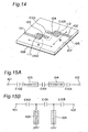
- Fig. 14 is a schematic view of a typical distributed element filter circuit.
- This filter circuit has a microstrip line as a high-frequency transmission line on which the distributed element is based.
- a dielectric substrate 105 that includes a dielectric 107 made of ceramic or the like, a GND pattern 108 on the lower surface of the dielectric substrate 107, an input port 101 and an output port 102.
- resonators 103 and 104 which are so-called the ⁇ /2 open-circuit line type resonators and in which the length of the microstrip line is designed to have a dimension of approximately ⁇ /2 with respect to a wavelength ⁇ of the center frequency of the filter
- a capacitance C101 shown in Fig. 14 is a capacitance component generated by a gap between the resonator 103 and the resonator 104.
- a capacitance C102 is a capacitance component generated by a gap between an input feed line 111 connected to an input port 101 and the ⁇ /2 resonator 103.
- a capacitance C103 is a capacitance component generated by a gap between an output feed line 112 connected to the output port 102 and the ⁇ /2 resonator 104.
- Distributed constant filter circuits as shown in this Fig. 14, which have been able to form a filter circuit of only one-layer printed wiring, easy to manufacture and able to restrain the cost low, have been frequently used in the frequency band of about 5 to 30 GHz. Further, the distributed element filter circuits as described above have recently been found here and there as examples used in the millimeter wave band of 30 to 60 GHz.
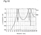
- the filter circuit shown in this Fig. 14 has an equivalent circuit as shown in Fig. 15A. It is further known that its filter characteristics generally become as shown in Fig. 16.
- the equivalent circuit shown in Fig. 15B is obtained by folding double the ⁇ /2 open-circuit line resonators 103 and 104 of the equivalent circuit shown in Fig. 15A taking advantage of the phenomenon that its center has a potential equal to that of the GND (ground) at and around the resonance frequency.
- the characteristics shown in Fig. 16 are the results of designing the equivalent circuit shown in Fig. 15A by means of a circuit simulator on the market with the center frequency set at 12 GHz.
- the characteristics of the high-frequency circuit are usually expressed by S parameters. That is, the characteristics are expressed by a parameter S11 that represents a reflection coefficient and a parameter S21 that represents a transmission coefficient.
- the filter circuit of the prior art shown in Fig. 14 has the following three problems i), ii) and iii).
- the first problem has been the low degree of steepness of the filter characteristics.
- the parameter S21 which represents the transmission coefficient, has no transmission zero and has a gently sloping bandpass characteristic in this filter.
- a parasitic passband is disadvantageously generated at a frequency double that of the proper passband. This also becomes a cause of the aforementioned first problem.
- the characteristics of Fig. 16 are the results of designing with the center frequency set at 12 GHz. As is clear with reference to the transmission coefficient parameter S21, a second passband is generated at and around 24 GHz, or the frequency double this center frequency.
- This second passband is a parasitic passband generated by the secondary resonance of the ⁇ /2 open-circuit line type resonators 103 and 104.
- the transmission coefficient parameter S21 in the frequency band of 12 GHz to 24 GHz increases as a whole due to this parasitic passband, and the attenuation value is degraded particularly at and around the frequencies of 12 GHz and 24GHz.
- the conventional millimeter wave band communication apparatus has been constructed of a local oscillator 201, a balance type mixer 202, an amplifier 203 and an antenna 204, and there has been often employed a balance type image rejection mixer 202 constructed of two mixers 205 and 206 instead of the filter for the purpose of image rejection.
- the reason for the above is the difficulties in achieving a degree of steepness required for the image rejection in the millimeter wave band in the prior art filter circuit that has no transmission zero as shown in Fig. 14.
- the balance type image rejection mixer has generally had a drawback that the bandwidth has been narrow, and it has been difficult to satisfy the demand of the system that has had a bandwidth of, for example, up to 2 to 3 GHz only by the balance type image rejection mixer.
- the balance type image rejection mixer it is usual that the chip area is enlarged double or more in comparison with the normal mixer circuit that is not the balance type. This has disadvantageously caused an increase in the chip unit price and difficulties in integrating any more other circuits (amplifier circuit and the like) on an identical chip.
- a waveguide filter 303 has often been employed as a filter capable of obtaining high performance even in the millimeter wave band for the purpose of image rejection, as shown in Fig. 17B.
- a waveguide filter 303 has often been employed as a filter capable of obtaining high performance even in the millimeter wave band for the purpose of image rejection, as shown in Fig. 17B.
- the drawbacks of difficulties in electrical connection between the waveguide that constitutes the waveguide filter 303 and the MMIC that constitutes the mixer 302 and the amplifier 304 as well as the expensiveness, large size and heavy weight of the waveguide filter 303 itself.
- the object of this invention is to solve the aforementioned problems and provide a compact area-saving easily manufacturable high-frequency filter circuit, monolithic microwave integrated circuit and high-frequency communication apparatus, which is suitable for producing an MMIC and in which the higher region side of the passband is steeply sloped by a transmission zero, generating no parasitic passband at a frequency double that of the passband.
- a high-frequency filter circuit wherein a first resonator and a second resonator are capacitively coupled to each other by a first capacitance, one terminal of the first resonator is capacitively coupled to an input port by a second capacitance, one terminal of the second resonator is capacitively coupled to an output port by a third capacitance, the other terminal of the first resonator is capacitively coupled to the output port by a fourth capacitance, and the other terminal of the second resonator is capacitively coupled to the input port by a fifth capacitance.
- the other terminal of the first resonator is capacitively coupled to the output port by the fourth capacitance, while the other terminal of the second resonator is capacitively coupled to the input port by the fifth capacitance. That is, the fourth capacitance capacitively couples the first resonator to the output port bypassing the first capacitance, the second resonator and the third capacitance.
- the fifth capacitance capacitively couples the second resonator to the input port bypassing the first capacitance, the first resonator and the second capacitance.
- the first resonator is directly capacitively coupled to the output port by the existence of this fourth capacitance, while the second resonator is directly capacitively coupled to the input port by the existence of the fifth capacitance.
- the first resonator is comprised of a first line
- the second resonator is comprised of a second line
- the first resonator and the second resonator are coupled to each other by the first capacitance with the first line facing the second line at a prescribed distance
- the input port is coupled to the first resonator by the second capacitance with a third line that includes the input port facing the first line
- the input port is coupled to the second resonator by the fifth capacitance with the third line facing the second line
- the output port is coupled to the second resonator by the third capacitance with a fourth line that includes the output port facing the second line
- the output port is coupled to the first resonator by the fourth capacitance with the fourth line facing the first line.
- the output port is coupled to the first resonator by the fourth capacitance in a jump coupling manner.
- the third line that includes the input port face the second line that constitutes the second resonator, the input port is coupled to the second resonator by the fifth capacitance in a jump coupling manner.
- the fourth and fifth capacitances for effecting the jump coupling can be constructed of the third and fourth lines that constitute the input and output ports.
- the embodiment is provided by devising the line arrangement in the vicinity of the resonators. Therefore, a bandpass filter circuit, in which the higher region side of the passband is steeply sloped by the transmission zero, can easily be provided by a simple circuit structure.
- a compact, area-saving and easily manufacturable high-frequency filter circuit which can be minimized in size by removing the dead space and is also suitable for producing an MMIC.
- a length of a confronting portion where the first line faces the second line is set within a range of 15% to 20% of a wavelength of a center frequency of a passband.
- the parasitic passband in the frequency band double that of the passband is suppressed. If the length of the confronting portion is out of the above-mentioned range, the parasitic passband cannot be suppressed.
- the high-frequency filter circuit of the present invention is integrally formed on an identical semiconductor substrate together with an amplifier circuit or a mixer circuit.
- a one-chip up-converter MMIC can be provided.
- the cost reduction, downsizing and weight reduction of the single unit of the filter circuit there can also be obtained the synergistic effects of achieving the remarkable simplification of the whole system, the reduction in the number of components and the simplification of the manufacturing processes.
- a high-frequency radio communication apparatus which has the high-frequency filter circuit of the present invention as a spurious rejection filter.
- a high-frequency radio communication apparatus having the spurious rejection filter, which can suppress the parasitic passband in the frequency band double that of the passband.
- Fig. 1 shows an equivalent circuit diagram of the first embodiment of the high-frequency filter circuit of this invention.
- this first embodiment one example of the 12-GHz band high-frequency filter is shown. The principle of the generation of a transmission zero on the higher region side of the passband of this high-frequency filter will be described with reference to the equivalent circuit of this Fig. 1.
- a first resonator 3 and a second resonator 4 are capacitively coupled to each other by a first capacitance C1.
- One terminal 3A of the first resonator 3 is capacitively coupled to an input port 1 via a second capacitance C2.
- One terminal 4A of the second resonator 4 is capacitively coupled to an output port 2 via a third capacitance C3.
- the other terminal 3B of the first resonator 3 is capacitively coupled to the output port 2 via a fourth capacitance C4.
- the other terminal 4B of the second resonator 4 is capacitively coupled to the input port 1 via a fifth capacitance C5.
- the equivalent circuit of this Fig. 1 has a circuit configuration in which jump coupling capacitances C4 and C5 are newly added to the equivalent circuit of Fig. 15A.
- This fourth capacitance C4 is the capacitance for coupling the other terminal 3B of the first resonator 3 to the output port 2 jumping over (bypassing) the first capacitance C1, the second resonator 4 and the third capacitance C3.
- the fifth capacitance C5 is the capacitance for coupling the other terminal 4B of the second resonator 4 to the input port 1 jumping over (bypassing) the first capacitance C1, the first resonator 3 and the second capacitance C2.
- Fig. 2 shows one example of the result of simulating the response of the filter circuit shown in Fig. 1 (transmission coefficient S21 and reflection coefficient S11) performed by a circuit simulator on the market.
- transmission coefficient S21 and reflection coefficient S11 transmission coefficient S21 and reflection coefficient S11
- Fig. 2 shows one example of the result of simulating the response of the filter circuit shown in Fig. 1 (transmission coefficient S21 and reflection coefficient S11) performed by a circuit simulator on the market.
- the first and second resonators 3 and 4 had a characteristic impedance of 10 ⁇ , and the electrical length at a frequency of 12 GHz was set at 167 degrees.
- Fig. 3 shows one example of the actual layout of the equivalent circuit of Fig. 1 as a microstrip line circuit on a 0.47-mm thick PPO (polypropylene oxide) substrate 10.
- the lower surface side of this substrate 10 is entirely a grounding layer (not shown).
- this microstrip line circuit is constructed of a third line 31 that includes the input port 1, a first line 32 that constitutes the first resonator 3, a second line 33 that constitutes the second resonator 4 and a fourth line 34 that includes the output port 2.
- These lines 31, 32, 33 and 34 are entirely strip-shaped lines that have the widths in the Y-direction of Fig. 3 and are extended in the X-direction (lengthwise direction).
- the line 32 is displaced in the X-direction and the Y-direction with respect to the line 31, whereas the line 32 and the line 31 have a section along which the lines face each other in the Y-direction.
- the line 33 is displaced in the X-direction and the reverse Y-direction with respect to the line 32, whereas the line 33 and the line 32 have a section along which the lines face each other in the Y-direction.
- the line 33 and the line 31 do not face each other in the Y-direction but face each other in the X-direction.
- the line 34 is displaced in the X-direction and the Y-direction with respect to the line 33, whereas the line 34 and the line 33 have a section along which the lines face each other in the Y-direction.
- the line 34 and the line 32 do not face each other in the Y-direction but face each other in the X-direction.
- the strip-shaped line 31 is constructed of a portion 31a that constitutes the input port 1 and a portion 31b that constitutes an input feed line 11.
- the width in the Y-direction of the portion 31b of this line 31 is approximately a half smaller than the width in the Y-direction of the portion 31a.
- This portion 31b of this line 31 faces a portion 32a of the line 32 at a prescribed distance in the Y-direction.
- This portion 31b and the portion 32a constitute the second capacitance C2.
- This line 32 constitutes the first resonator 3, which is a ⁇ /2 (1/2 wavelengths) open-circuit line type resonator.
- the portion 32b of this line 32 faces a portion 33a of the line 33 at a prescribed distance.
- An overlap distance over which this portion 33a and the portion 32b face each other is assumed to be L.
- This line 33 constitute the second resonator 4, which is a ⁇ /2 open-circuit line type resonator.
- the portion 33b of this line 33 faces a portion 34a that constitutes the output feed line of the line 34 at a prescribed distance in the Y-direction.
- This portion 33b and the portion 34a constitute the third capacitance C3.
- the portion 34b of this line 34 constitutes the output port 2.
- the width in the Y-direction of the portion 34a is approximately a half of the width in the Y-direction of the portion 34b.
- the portions 31a, 32a, 32b, 33a, 33b and 34b have approximately same widths in the Y-direction.
- an end portion 34a-1 of the portion 34a of this line 34 is adjacent to an end portion 32b-1 of the portion 32b of the line 32 at prescribed distances in the X-direction and the Y-direction.
- This end portion 34a-1 and the end portion 32b-1 constitute the fourth capacitance C4.
- the end portion 33a-1 of the portion 33a of the line 33 is adjacent to the end portion 31b-1 of the portion 31b of the line 31 at prescribed distances in the X-direction and the Y-direction.
- This end portion 33a-1 and the end portion 31b-1 constitute the fifth capacitance C5.
- the fourth capacitance C4 for jump coupling is provided by arranging the open end 32b-1 located on the side opposite to the input port 1 of the line 32 that constitutes the resonator 3 close to the open end 34a-1 of the line 34 that constitutes the output port 2.
- the other capacitance C5 for jump coupling is provided by arranging the open end 33a-1 located on the side opposite to the output port 2 of the line 33 that constitutes the resonator 4 close to the open end 31b-1 of the line 31 that constitutes the input port 1.
- minimum Line/Space (line and space) was set at 200 ⁇ m, and the lengths in the X-direction of the ⁇ /2 resonators 3 and 4 were set at about 4.6 mm.
- the dimension L shown in Fig. 3 is the overlap distance of the arrangement of the two ⁇ /2 resonators 3 and 4, i.e., the dimension L is the length along which the lines 32 and 33 face each other in the Y-direction.
- the length L was a half of the resonator length (dimensions in the X-direction of the lines 32 and 33), i.e., about ⁇ /4 (1/4 wavelengths) in Fig. 3.
- the two resonator lines 32 and 33 and the two input/output lines 31 and 34 are arranged closer to each other than in the conventional structure as shown in Fig. 14, generating almost no dead space. Therefore, area saving can be achieved, and this arrangement is also suitable for use in the case of monolithic integration on a millimeter wave MMIC (monolithic microwave integrated circuit).
- MMIC monolithic microwave integrated circuit
- Fig. 4 shows the result of simulating the circuit of the line layout shown in Fig. 3 by a moment method electromagnetic field simulator on the market.
- transmission zeros p11 and p12 are generated on the higher region side of the passband (12 GHz), and the degree of steepness is improved.
- a parasitic passband P13 is generated at a frequency (24 GHz) double that of the passband (12 GHz), degrading the attenuation value.
- the attenuation value in this band of the doubled frequency can be improved by the method described as follows, if necessary.
- Fig. 5 shows this behavior in the form of a graph based on an electromagnetic field simulation result.
- the horizontal axis represents a value obtained by dividing the overlap distance L in Fig.
- the transmission coefficient S21 in the band of 21 to 24 GHz (at and around 2f 0 ) can be reduced when the distance L is 15 to 20% of the wavelength ⁇ at the center frequency f 0 of the filter.
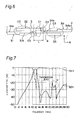
- Fig. 6 shows a line layout, in which the overlap distances L between the resonators is shortened to about ⁇ /6 of the line layout shown in Fig. 3, on the basis of this principle.
- the length along which the line 31 and the line 32 face each other in the Y-direction and the length along which the line 33 and the line 34 face each other in the Y-direction are made longer than those of the layout of Fig. 3 in accordance with the arrangement that the overlap distances L between the resonators is shortened to about ⁇ /6.
- Fig. 7 shows the actual measurement result of a sample of a microstrip line circuit that adopts the line layout of this Fig. 6, the sample being actually produced on an experimental basis.
- the transmission coefficient S21 that represents the attenuation value at the frequency (24-GHz band) double that of the passband (12-GHz band) is improved to about 20 dB at worst.
- a probing pad of GSG ground signal ground (coplanar)
- VAA via
- LRM line reflect match
- Fig. 1 shows the principle of this invention, and this invention can also be applied to a circuit of another high-frequency strip line, such as a concentrated constant circuit and a coplanar line.
- the line widths of the terminal end portions 31b and 34a of the input/output lines 31 and 34 were made thinner in comparison with the portions 31a and 34b. This configuration was adopted for impedance matching.
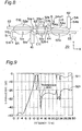
- Fig. 8 shows the second embodiment of the filter circuit of this invention.
- This second embodiment has linear strip lines 52 and 53 and bent strip lines 51 and 54.
- the strip lines 51 and 52 face each other at a prescribed distance in the Y-direction, while the strip lines 52 and 53 face each other at a prescribed distance in the Y-direction.
- the strip lines 53 and 54 face each other at a prescribed distance in the Y-direction.
- This strip line 52 constitutes a first resonator 63, while the strip line 53 constitutes a second resonator 64.
- This first resonator 63 and the second resonator 64 correspond to the first resonator 3 and the second resonator 4, respectively, of the equivalent circuit of Fig. 1.
- the line 51 has a portion 51a that constitutes an input port 61, a portion 51b and a portion 51c that faces a portion 52a of the line 52.
- the portion 51a and the portion 51b extend in the reverse Y-direction from both ends of the portion 51c.
- this portion 51b has its terminal end portion 51b-1 that constitutes an open end 65 bent in the X-direction.
- a basal end 51a-1 of this portion 51a faces a terminal end portion 53a-1 of the portion 53a of the line 53 at a prescribed distance in the X-direction.
- ends 51a-1 and 53a-1 constitute a fifth capacitance C15 that serves as a jump coupling capacitance, while the portion 51c and the portion 52a constitute a second capacitance C12.
- This fifth capacitance C15 and the second capacitance C12 correspond to the capacitances C5 and C2, respectively, of the equivalent circuit of Fig. 1.
- the portion 52b of the line 52 faces the portion 53a of the line 53 at a prescribed distance in the reverse Y-direction, while this portion 52b and the portion 53a constitute a first capacitance C11.
- a portion 53b of the line 53 faces a portion 54c of the lines 54 at a prescribed distance in the Y-direction, while this portion 53b and the portion 54c constitute a third capacitance C13.
- This first capacitance C11 and the third capacitance C13 correspond to the capacitance C1 and the capacitance C3, respectively, of the equivalent circuit of Fig. 1.
- this line 54 has portions 54a and 54b that extend in the Y-direction from both ends of the portion 54c.
- This portion 54a faces an end portion 52b-1 of the portion 52b of the line 52 at a prescribed distance in the reverse X-direction, while this portion 54a and the end portion 52b-1 constitute a fourth capacitance C14.
- This fourth capacitance C14 corresponds to the capacitance C4 of the equivalent circuit of Fig. 1.
- the portion 54b of this line 54 constitutes an output port 62.
- the portion 51a of the line 51 that constitutes the input port 61 is bent approximately perpendicularly to the portion 51c
- the portion 51b of the line 51 is bent approximately perpendicularly from the portion 51c
- the open end 65 is bent approximately perpendicularly from the portion 51b.
- the dimension in the X-direction of the occupation region on a substrate 70 can be reduced. Therefore, this arrangement enables the layout in a free space that has a short dimension in the X-direction on the substrate. Therefore, area saving and downsizing can be achieved by reducing the dead space on the surface of the substrate 70. Therefore, monolithic integration can also be achieved by utilizing a free space on the MMIC of another circuit.
- Fig. 9 shows the electromagnetic field simulation result of the circuit of this second embodiment.
- the attenuation value at the frequency (24-GHz band) double that of the passband (12-GHz band) is improved to about 20 dB at worst, similarly to the frequency characteristic (Fig. 7) of the S parameters of the modification example of the aforementioned first embodiment.
- S11 represents the reflection coefficient.
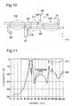
- Fig. 10 shows the third embodiment, which is a modification example of the aforementioned second embodiment.
- This third embodiment differs from the second embodiment in that the strip line 54 of the second embodiment of Fig. 8 is arranged in a state in which it is rotated by 180° around the Y-direction axis that extends through its center of the X-direction. That is, this third embodiment has a strip line 81 obtained by changing the coupling direction of the strip line 54 that constitutes the output line in Fig. 8.
- the dimension in the Y-direction at the end in the X-direction can be made smaller than that of the second embodiment.
- the dimension in the Y-direction at the center portion in the X-direction becomes greater than that of the second embodiment. Therefore, according to this third embodiment, the lines can be arranged in a free space of which the dimension in the Y-direction at both ends in the X-direction is shorter than that of the second embodiment.
- Fig. 11 shows the electromagnetic field simulation result of the circuit of this third embodiment.
- the transmission coefficient S21 that represents the attenuation value at the frequency (24-GHz band) double that of the passband (12-GHz band) is about 10 dB at worst. It is to be noted that S11 represents the reflection coefficient.
- the filter circuit of the first through third embodiments is monolithically integrated on a millimeter wave band MMIC, then the resulting device is suitable for use in performing spurious rejection.
- the high-frequency filter circuit of the aforementioned embodiment as a filter for rejecting, for example, the image signal and the local signal.
- the characteristic impedance of the first resonator 3 and the second resonator 4 were set at 12 ⁇ , and the electrical lengths at a frequency of 60 GHz was set at 162 degrees.
- a bandwidth F1 of about 2.5 GHz was able to be secured in the 60-GHz band, or the passband.
- the filter of this invention a bandwidth of 2 to 3 GHz in the 60-GHz band can easily be secured.
- the filter circuit itself is small, it is easy to further integrate another circuit (amplifier circuit or the like) on an identical chip.
- the filter of this invention can easily be monolithically integrated with the amplifier circuit and the mixer circuit located before and behind it on an MMIC, and the filter itself is low-cost, microminiature and ultralight.
- Fig. 13 shows the construction of a monolithic. microwave integrated circuit of the fourth embodiment of this invention.
- This fourth embodiment is provided with the filter circuit of the aforementioned modification example (Fig. 6) of the first embodiment as an image rejection filter circuit 84.
- This fourth embodiment constitutes the aforementioned multi-channel TV signal transmission system.
- a TV signal inputted to a mixer circuit 82 is mixed with a local oscillation signal from a local oscillator 83, and a signal from this mixer circuit 82 is inputted to an amplifier circuit 85 via the filter circuit 84, amplified and transmitted from an antenna 86.
- this fourth embodiment is the so-called "one-chip up-converter MMIC" in which the mixer circuit 82, the filter circuit 84, the amplifier circuit 85 and the local oscillator circuit 83 are all formed on an identical chip 81.
- the chip 81 may be divided into about two MMIC chips according to the convenience of manufacturing and design.
- the filter circuit of the aforementioned first, second or third embodiment the system can be entirely formed of an MMIC. Accordingly, in addition to the cost reduction, downsizing and weight reduction of the single unit of the filter circuit, there can also be obtained the synergistic effects of achieving the remarkable simplification of the whole system, the reduction in the number of components and the simplification of the manufacturing processes.
- Fig. 1 shows the principle of this invention, and this invention can alsp be applied to a circuit of other high-frequency lines, such as a concentrated constant circuit and a coplanar line.
Landscapes
- Physics & Mathematics (AREA)
- Electromagnetism (AREA)
- Control Of Motors That Do Not Use Commutators (AREA)
- Waveguides (AREA)
Abstract
In this high-frequency filter circuit, a fourth
capacitance C4 capacitively couples a first resonator 3 to
an output port 2 bypassing a first capacitance C1, a second
resonator 4 and a third capacitance C3, while a fifth
capacitance C5 capacitively couples a second resonator 4 to
an input port 1 bypassing the first capacitance C1, the
first resonator 3 and a second capacitance C2. According
to this filter circuit, the first resonator 3 is directly
capacitively coupled to the output port 2 by the existence
of this fourth capacitance C4, while the second resonator 4
is directly capacitively coupled to the input port 1 by the
existence of the fifth capacitance C5. According to the
above-mentioned high-frequency filter circuit, there can
easily be manufactured a high-frequency filter circuit,
which is able to achieve downsizing and area saving and
suitable for producing an MMIC and in which the higher
region side of the passband is steeply sloped by a
transmission zero, generating no parasitic passband at a
frequency double that of the passband.
Description
The present invention relates to a high-frequency
filter circuit that constitutes, for example, a bandpass
filter and relates, in particular, to a high-frequency
filter circuit, a monolithic microwave integrated circuit
and a high-frequency communication apparatus, which
constitute a distributed element filter having a high-frequency
transmission line such as a microstrip line and a
coplanar line for use in a high-frequency band such as a
microwave band and a millimeter wave band.
Fig. 14 is a schematic view of a typical
distributed element filter circuit. This filter circuit
has a microstrip line as a high-frequency transmission line
on which the distributed element is based. In Fig. 14 are
shown a dielectric substrate 105 that includes a dielectric
107 made of ceramic or the like, a GND pattern 108 on the
lower surface of the dielectric substrate 107, an input
port 101 and an output port 102. There are further
provided resonators 103 and 104, which are so-called the
λ/2 open-circuit line type resonators and in which the
length of the microstrip line is designed to have a
dimension of approximately λ/2 with respect to a wavelength
λ of the center frequency of the filter
Both ends of these resonators 103 and 104 are
open ends. A capacitance C101 shown in Fig. 14 is a
capacitance component generated by a gap between the
resonator 103 and the resonator 104. A capacitance C102 is
a capacitance component generated by a gap between an input
feed line 111 connected to an input port 101 and the λ/2
resonator 103. A capacitance C103 is a capacitance
component generated by a gap between an output feed line
112 connected to the output port 102 and the λ/2 resonator
104.
Distributed constant filter circuits, as shown in
this Fig. 14, which have been able to form a filter circuit
of only one-layer printed wiring, easy to manufacture and
able to restrain the cost low, have been frequently used in
the frequency band of about 5 to 30 GHz. Further, the
distributed element filter circuits as described above have
recently been found here and there as examples used in the
millimeter wave band of 30 to 60 GHz.
The filter circuit shown in this Fig. 14 has an
equivalent circuit as shown in Fig. 15A. It is further
known that its filter characteristics generally become as
shown in Fig. 16. The equivalent circuit shown in Fig. 15B
is obtained by folding double the λ/2 open- circuit line
resonators 103 and 104 of the equivalent circuit shown in
Fig. 15A taking advantage of the phenomenon that its center
has a potential equal to that of the GND (ground) at and
around the resonance frequency.
The characteristics shown in Fig. 16 are the
results of designing the equivalent circuit shown in Fig.
15A by means of a circuit simulator on the market with the
center frequency set at 12 GHz. The characteristics shown
in this Fig. 16 are the results of simulation when the
capacitance C101 = 0.17145 pF, the capacitance C102 = C103
= 0.29200 pF, the characteristic impedance of the
resonators 103 and 104 is 10 Ω and the electrical length
at 12 GHz is 172 degrees.
As shown in Fig. 16, the characteristics of the
high-frequency circuit are usually expressed by S
parameters. That is, the characteristics are expressed by
a parameter S11 that represents a reflection coefficient
and a parameter S21 that represents a transmission
coefficient.
The filter circuit of the prior art shown in Fig.
14 has the following three problems i), ii) and iii).
That is, i) the first problem has been the low
degree of steepness of the filter characteristics. As is
apparent with reference to Fig. 16, the parameter S21,
which represents the transmission coefficient, has no
transmission zero and has a gently sloping bandpass
characteristic in this filter. In particular, it is more
difficult to achieve a steep attenuation characteristic on
the higher region side of the passband due to the second
problem described next.
ii) As the second problem, there is the problem
that a parasitic passband is disadvantageously generated at
a frequency double that of the proper passband. This also
becomes a cause of the aforementioned first problem. The
characteristics of Fig. 16 are the results of designing
with the center frequency set at 12 GHz. As is clear with
reference to the transmission coefficient parameter S21, a
second passband is generated at and around 24 GHz, or the
frequency double this center frequency.
This second passband is a parasitic passband
generated by the secondary resonance of the λ/2 open-circuit
line type resonators 103 and 104. There is a
tendency that the transmission coefficient parameter S21 in
the frequency band of 12 GHz to 24 GHz increases as a whole
due to this parasitic passband, and the attenuation value
is degraded particularly at and around the frequencies of
12 GHz and 24GHz.
iii) As the third problem, there has been the
problem of a large circuit area. Particularly when
producing a narrow-band bandpass filter, it is required to
reduce the degree of coupling (capacitance C101) by
expanding the gap between the resonators 103 and 104 in
Fig. 14, and a dead space is generated in the direction
indicated by arrow B in Fig. 14, causing an increased
dimension.
On the other hand, it is known that reducing the
number of components and the inter-circuit connecting
portions by integrating a plurality of circuits in a one-chip
form on an MMIC (monolithic microwave integrated
circuit) is a very effective technique in terms of
improving both the electrical performance and the
manufacturing cost in an ultra-high-frequency band such as
the millimeter wave band. This can also be said for the
filter circuit, and there is an intense demand for
integrating the filter circuit with an amplifier circuit
and a mixer circuit, which are connected before and behind
the filter circuit, in a one-chip form on the MMIC. In
particular, for the reduction in the chip cost of the MMIC,
it is required to reduce the circuit area as far as
possible by removing the dead space in the layout stage.
In contrast to this, it is difficult for the
prior art filter shown in Fig. 14 to reduce the chip cost
due to the obstacle of the large dead space in the
direction of arrow B in Fig. 14.
Therefore, as shown in Fig. 17A, for example, the
conventional millimeter wave band communication apparatus
has been constructed of a local oscillator 201, a balance
type mixer 202, an amplifier 203 and an antenna 204, and
there has been often employed a balance type image
rejection mixer 202 constructed of two mixers 205 and 206
instead of the filter for the purpose of image rejection.
The reason for the above is the difficulties in achieving a
degree of steepness required for the image rejection in the
millimeter wave band in the prior art filter circuit that
has no transmission zero as shown in Fig. 14. However, the
balance type image rejection mixer has generally had a
drawback that the bandwidth has been narrow, and it has
been difficult to satisfy the demand of the system that has
had a bandwidth of, for example, up to 2 to 3 GHz only by
the balance type image rejection mixer. Moreover, when the
balance type image rejection mixer is employed, it is usual
that the chip area is enlarged double or more in comparison
with the normal mixer circuit that is not the balance type.
This has disadvantageously caused an increase in the chip
unit price and difficulties in integrating any more other
circuits (amplifier circuit and the like) on an identical
chip.
In another case, a waveguide filter 303 has often
been employed as a filter capable of obtaining high
performance even in the millimeter wave band for the
purpose of image rejection, as shown in Fig. 17B. However,
in this case, there have been the drawbacks of difficulties
in electrical connection between the waveguide that
constitutes the waveguide filter 303 and the MMIC that
constitutes the mixer 302 and the amplifier 304, as well as
the expensiveness, large size and heavy weight of the
waveguide filter 303 itself.
Accordingly, the object of this invention is to
solve the aforementioned problems and provide a compact
area-saving easily manufacturable high-frequency filter
circuit, monolithic microwave integrated circuit and high-frequency
communication apparatus, which is suitable for
producing an MMIC and in which the higher region side of
the passband is steeply sloped by a transmission zero,
generating no parasitic passband at a frequency double that
of the passband.
In order to achieve the above object, there is
provided a high-frequency filter circuit wherein
a first resonator and a second resonator are capacitively coupled to each other by a first capacitance,
one terminal of the first resonator is capacitively coupled to an input port by a second capacitance,
one terminal of the second resonator is capacitively coupled to an output port by a third capacitance,
the other terminal of the first resonator is capacitively coupled to the output port by a fourth capacitance, and
the other terminal of the second resonator is capacitively coupled to the input port by a fifth capacitance.
a first resonator and a second resonator are capacitively coupled to each other by a first capacitance,
one terminal of the first resonator is capacitively coupled to an input port by a second capacitance,
one terminal of the second resonator is capacitively coupled to an output port by a third capacitance,
the other terminal of the first resonator is capacitively coupled to the output port by a fourth capacitance, and
the other terminal of the second resonator is capacitively coupled to the input port by a fifth capacitance.
In this invention, the other terminal of the
first resonator is capacitively coupled to the output port
by the fourth capacitance, while the other terminal of the
second resonator is capacitively coupled to the input port
by the fifth capacitance. That is, the fourth capacitance
capacitively couples the first resonator to the output port
bypassing the first capacitance, the second resonator and
the third capacitance. The fifth capacitance capacitively
couples the second resonator to the input port bypassing
the first capacitance, the first resonator and the second
capacitance.
As described above, according to this invention,
the first resonator is directly capacitively coupled to the
output port by the existence of this fourth capacitance,
while the second resonator is directly capacitively coupled
to the input port by the existence of the fifth
capacitance. By the so-called jump coupling as described
above, a transmission zero was able to be formed in the
frequency characteristic curve of the transmission
coefficient S21 of the S parameters, and the degree of
steepness of this frequency characteristic curve was able
to be increased, allowing the filter characteristics to be
improved.
In one embodiment of the present invention, the
first resonator is comprised of a first line, the second
resonator is comprised of a second line,
the first resonator and the second resonator are coupled to each other by the first capacitance with the first line facing the second line at a prescribed distance,
the input port is coupled to the first resonator by the second capacitance with a third line that includes the input port facing the first line,
the input port is coupled to the second resonator by the fifth capacitance with the third line facing the second line,
the output port is coupled to the second resonator by the third capacitance with a fourth line that includes the output port facing the second line, and
the output port is coupled to the first resonator by the fourth capacitance with the fourth line facing the first line.
the first resonator and the second resonator are coupled to each other by the first capacitance with the first line facing the second line at a prescribed distance,
the input port is coupled to the first resonator by the second capacitance with a third line that includes the input port facing the first line,
the input port is coupled to the second resonator by the fifth capacitance with the third line facing the second line,
the output port is coupled to the second resonator by the third capacitance with a fourth line that includes the output port facing the second line, and
the output port is coupled to the first resonator by the fourth capacitance with the fourth line facing the first line.
In this embodiment, by making the fourth line
that includes the output port face the first line that
constitutes the first resonator, the output port is coupled
to the first resonator by the fourth capacitance in a jump
coupling manner. Moreover, by making the third line that
includes the input port face the second line that
constitutes the second resonator, the input port is coupled
to the second resonator by the fifth capacitance in a jump
coupling manner.
As described above, in this embodiment, the
fourth and fifth capacitances for effecting the jump
coupling can be constructed of the third and fourth lines
that constitute the input and output ports. Without newly
adding any component, the embodiment is provided by
devising the line arrangement in the vicinity of the
resonators. Therefore, a bandpass filter circuit, in which
the higher region side of the passband is steeply sloped by
the transmission zero, can easily be provided by a simple
circuit structure. Moreover, with the above-mentioned line
arrangement, there can be provided a compact, area-saving
and easily manufacturable high-frequency filter circuit,
which can be minimized in size by removing the dead space
and is also suitable for producing an MMIC.
In one embodiment of the present invention, a
length of a confronting portion where the first line faces
the second line is set within a range of 15% to 20% of a
wavelength of a center frequency of a passband.
In the high-frequency filter circuit of this
embodiment, by setting the length of the confronting
portion where the first line that constitutes the first
resonator face the second line that constitutes the second
resonator within the range of 15% to 20% of the wavelength
of the center frequency of the passband, the parasitic
passband in the frequency band double that of the passband
is suppressed. If the length of the confronting portion is
out of the above-mentioned range, the parasitic passband
cannot be suppressed.
In one embodiment of the present invention, the
high-frequency filter circuit of the present invention is
integrally formed on an identical semiconductor substrate
together with an amplifier circuit or a mixer circuit.
According to the monolithic microwave integrated
circuit of this embodiment, by integrally forming the high-frequency
filter circuit on an identical semiconductor
substrate together with an amplifier circuit or a mixer
circuit, a one-chip up-converter MMIC can be provided. In
addition to the cost reduction, downsizing and weight
reduction of the single unit of the filter circuit, there
can also be obtained the synergistic effects of achieving
the remarkable simplification of the whole system, the
reduction in the number of components and the
simplification of the manufacturing processes.
In one embodiment of the present invention, a
high-frequency radio communication apparatus, which has the
high-frequency filter circuit of the present invention as a
spurious rejection filter.
According to this embodiment, there can be
provided a high-frequency radio communication apparatus
having the spurious rejection filter, which can suppress
the parasitic passband in the frequency band double that of
the passband.
The present invention will become more fully
understood from the detailed description given hereinbelow
and the accompanying drawings which are given by way of
illustration only, and thus are not limitative of the
present invention, and wherein:
The embodiments of this invention will be
described more concretely in detail below with reference to
the drawings.
Fig. 1 shows an equivalent circuit diagram of the
first embodiment of the high-frequency filter circuit of
this invention. In this first embodiment, one example of
the 12-GHz band high-frequency filter is shown. The
principle of the generation of a transmission zero on the
higher region side of the passband of this high-frequency
filter will be described with reference to the equivalent
circuit of this Fig. 1.
In the equivalent circuit of this first
embodiment, a first resonator 3 and a second resonator 4
are capacitively coupled to each other by a first
capacitance C1. One terminal 3A of the first resonator 3
is capacitively coupled to an input port 1 via a second
capacitance C2. One terminal 4A of the second resonator 4
is capacitively coupled to an output port 2 via a third
capacitance C3.
The other terminal 3B of the first resonator 3 is
capacitively coupled to the output port 2 via a fourth
capacitance C4. The other terminal 4B of the second
resonator 4 is capacitively coupled to the input port 1 via
a fifth capacitance C5.
Neither the fourth capacitance C4 nor the fifth
capacitance C5 exists in the equivalent circuit of the
prior art of Fig. 15A. That is, the equivalent circuit of
this Fig. 1 has a circuit configuration in which jump
coupling capacitances C4 and C5 are newly added to the
equivalent circuit of Fig. 15A. This fourth capacitance C4
is the capacitance for coupling the other terminal 3B of
the first resonator 3 to the output port 2 jumping over
(bypassing) the first capacitance C1, the second resonator
4 and the third capacitance C3. The fifth capacitance C5
is the capacitance for coupling the other terminal 4B of
the second resonator 4 to the input port 1 jumping over
(bypassing) the first capacitance C1, the first resonator 3
and the second capacitance C2.
Next, Fig. 2 shows one example of the result of
simulating the response of the filter circuit shown in Fig.
1 (transmission coefficient S21 and reflection coefficient
S11) performed by a circuit simulator on the market.
Referring to the response characteristic of this Fig. 2,
dissimilarly to the response characteristic of the prior
art shown in Fig. 16, it can be understood that
transmission zeros p1 and p2 are generated on the higher
region side of the passband (11.5 to 12 GHz) and the degree
of steepness is greatly improved. The simulation result
shown in Fig. 2 was calculated on the following parameter
conditions. The conditions were: C1 (first capacitance) =
0.22843 pF, C2 (second capacitance) = C3 (third
capacitance) = 0.33561 pF, and C4 (fourth capacitance) = C5
(fifth capacitance) = 0.05821 pF. The first and second
resonators 3 and 4 had a characteristic impedance of 10 Ω,
and the electrical length at a frequency of 12 GHz was set
at 167 degrees.
In this first embodiment, as is apparent from the
response characteristic simulation result of Fig. 2, the
problem that the degree of steepness on the higher region
side is low, or the first problem out of the aforementioned
three problems of the prior art, can be solved. This fact
can be explained by the equivalent circuit shown in Fig. 1.
Next, the second and third problems of the prior
art are closely related to the line layout that constitutes
the high-frequency filter circuit. Therefore, it is
difficult to provide an explanation with the abstract
equivalent circuit.
Therefore, the explanation is continued by means
of characteristic charts (Figs. 4 and 5) that show the
calculation results of an electromagnetic field simulator
on the market by the moment method as follows. A
characteristic chart (Fig. 7) is not a simulation result
but an actual measurement result.
Fig. 3 shows one example of the actual layout of
the equivalent circuit of Fig. 1 as a microstrip line
circuit on a 0.47-mm thick PPO (polypropylene oxide)
substrate 10. The lower surface side of this substrate 10
is entirely a grounding layer (not shown). In Fig. 3, only
the electrode pattern on the upper surface side of the
substrate 10 is shown. As shown in Fig. 3, this microstrip
line circuit is constructed of a third line 31 that
includes the input port 1, a first line 32 that constitutes
the first resonator 3, a second line 33 that constitutes
the second resonator 4 and a fourth line 34 that includes
the output port 2. These lines 31, 32, 33 and 34 are
entirely strip-shaped lines that have the widths in the Y-direction
of Fig. 3 and are extended in the X-direction
(lengthwise direction).
As shown in Fig. 3, the line 32 is displaced in
the X-direction and the Y-direction with respect to the
line 31, whereas the line 32 and the line 31 have a section
along which the lines face each other in the Y-direction.
The line 33 is displaced in the X-direction and the reverse
Y-direction with respect to the line 32, whereas the line
33 and the line 32 have a section along which the lines
face each other in the Y-direction. The line 33 and the
line 31 do not face each other in the Y-direction but face
each other in the X-direction. The line 34 is displaced in
the X-direction and the Y-direction with respect to the
line 33, whereas the line 34 and the line 33 have a section
along which the lines face each other in the Y-direction.
The line 34 and the line 32 do not face each other in the
Y-direction but face each other in the X-direction.
The strip-shaped line 31 is constructed of a
portion 31a that constitutes the input port 1 and a portion
31b that constitutes an input feed line 11. The width in
the Y-direction of the portion 31b of this line 31 is
approximately a half smaller than the width in the Y-direction
of the portion 31a.
The portion 31b of this line 31 faces a portion
32a of the line 32 at a prescribed distance in the Y-direction.
This portion 31b and the portion 32a constitute
the second capacitance C2. This line 32 constitutes the
first resonator 3, which is a λ/2 (1/2 wavelengths) open-circuit
line type resonator.
Moreover, the portion 32b of this line 32 faces a
portion 33a of the line 33 at a prescribed distance. An
overlap distance over which this portion 33a and the
portion 32b face each other is assumed to be L. This line
33 constitute the second resonator 4, which is a λ/2 open-circuit
line type resonator. Moreover, the portion 33b of
this line 33 faces a portion 34a that constitutes the
output feed line of the line 34 at a prescribed distance in
the Y-direction. This portion 33b and the portion 34a
constitute the third capacitance C3. Moreover, the portion
34b of this line 34 constitutes the output port 2. The
width in the Y-direction of the portion 34a is
approximately a half of the width in the Y-direction of the
portion 34b. Moreover, the portions 31a, 32a, 32b, 33a,
33b and 34b have approximately same widths in the Y-direction.
Further, an end portion 34a-1 of the portion 34a
of this line 34 is adjacent to an end portion 32b-1 of the
portion 32b of the line 32 at prescribed distances in the
X-direction and the Y-direction. This end portion 34a-1
and the end portion 32b-1 constitute the fourth capacitance
C4. Further, the end portion 33a-1 of the portion 33a of
the line 33 is adjacent to the end portion 31b-1 of the
portion 31b of the line 31 at prescribed distances in the
X-direction and the Y-direction. This end portion 33a-1
and the end portion 31b-1 constitute the fifth capacitance
C5.
That is, the fourth capacitance C4 for jump
coupling is provided by arranging the open end 32b-1
located on the side opposite to the input port 1 of the
line 32 that constitutes the resonator 3 close to the open
end 34a-1 of the line 34 that constitutes the output port
2. Moreover, the other capacitance C5 for jump coupling is
provided by arranging the open end 33a-1 located on the
side opposite to the output port 2 of the line 33 that
constitutes the resonator 4 close to the open end 31b-1 of
the line 31 that constitutes the input port 1.
In this one example, minimum Line/Space (line and
space) was set at 200 µm, and the lengths in the X-direction
of the λ/2 resonators 3 and 4 were set at about
4.6 mm. The dimension L shown in Fig. 3 is the overlap
distance of the arrangement of the two λ/2 resonators 3 and
4, i.e., the dimension L is the length along which the
lines 32 and 33 face each other in the Y-direction. In
Fig. 3, the length L was a half of the resonator length
(dimensions in the X-direction of the lines 32 and 33),
i.e., about λ/4 (1/4 wavelengths) in Fig. 3.
As described above, in the filter circuit of this
first embodiment, the two resonator lines 32 and 33 and the
two input/ output lines 31 and 34 are arranged closer to
each other than in the conventional structure as shown in
Fig. 14, generating almost no dead space. Therefore, area
saving can be achieved, and this arrangement is also
suitable for use in the case of monolithic integration on a
millimeter wave MMIC (monolithic microwave integrated
circuit).
Next, Fig. 4 shows the result of simulating the
circuit of the line layout shown in Fig. 3 by a moment
method electromagnetic field simulator on the market.
Referring to Fig. 4, similarly to the equivalent circuit
simulation result shown in Fig. 2, transmission zeros p11
and p12 are generated on the higher region side of the
passband (12 GHz), and the degree of steepness is improved.
Also, according to the characteristic of this Fig. 4,
similarly to the equivalent circuit simulation result shown
in Fig. 2, a parasitic passband P13 is generated at a
frequency (24 GHz) double that of the passband (12 GHz),
degrading the attenuation value.
Accordingly, in the filter circuit of this
embodiment, the attenuation value in this band of the
doubled frequency can be improved by the method described
as follows, if necessary.
That is, by adjusting the overlap distance L
between the two λ/2 resonators 3 and 4 (distance between
the lines 32 and 33 facing each other in the Y-direction)
in the circuit of the construction shown in Fig. 3, the
attenuation value in the band of the doubled frequency of
the filter characteristic shown in Fig. 4 (region P13 in
Fig. 4) changes. Fig. 5 shows this behavior in the form of
a graph based on an electromagnetic field simulation
result. In this Fig. 5, the horizontal axis represents a
value obtained by dividing the overlap distance L in Fig. 3
by a wavelength λ at a center frequency f0 of the passband,
while the vertical axis represents the worst value (maximum
value) of the transmission coefficient S21 in the band of
21 to 24 GHz. It can be understood that the transmission
coefficient S21 in the band of 21 to 24 GHz (at and around
2f0) can be reduced when the distance L is 15 to 20% of the
wavelength λ at the center frequency f0 of the filter.
Fig. 6 shows a line layout, in which the overlap
distances L between the resonators is shortened to about
λ/6 of the line layout shown in Fig. 3, on the basis of
this principle.
In the line layout shown in this Fig. 6, the
overlap distances L between the resonators (distance
between the lines 32 and 33 facing each other in the Y-direction),
is shortened to about λ/6 in comparison with
the line layout of Fig. 3. However, the distance between
the line 32 and the line 33 in the Y-direction is same.
Moreover, according to the layout of Fig. 6, the positional
relation between the line 31 and the line 33 and the
positional relation between the line 32 and the line 34 are
not changed from the layout of Fig. 3. Moreover, according
to the layout of Fig. 6, the length along which the line 31
and the line 32 face each other in the Y-direction and the
length along which the line 33 and the line 34 face each
other in the Y-direction are made longer than those of the
layout of Fig. 3 in accordance with the arrangement that
the overlap distances L between the resonators is shortened
to about λ/6.
Fig. 7 shows the actual measurement result of a
sample of a microstrip line circuit that adopts the line
layout of this Fig. 6, the sample being actually produced
on an experimental basis. Referring to the region P
encircled by the dashed line in Fig. 7, it can be
understood that the transmission coefficient S21 that
represents the attenuation value at the frequency (24-GHz
band) double that of the passband (12-GHz band) is improved
to about 20 dB at worst. According to the measuring
method, a probing pad of GSG (ground signal ground
(coplanar)) obtained by adding a via (VIA) hole to the
terminal end portion of the input/output microstrip line of
the substrate produced on an experimental basis was
provided, and the S parameters were measured by a network
analyzer with a coplanar high-frequency probe, which had
undergone LRM (line reflect match) calibration, applied to
the probing pad.
In this embodiment, the example of the microstrip
line circuit of the distributed element type has been
described. However, the equivalent circuit of Fig. 1 shows
the principle of this invention, and this invention can
also be applied to a circuit of another high-frequency
strip line, such as a concentrated constant circuit and a
coplanar line.
According to the layouts shown in Figs. 3 and 6,
the line widths of the terminal end portions 31b and 34a of
the input/ output lines 31 and 34 were made thinner in
comparison with the portions 31a and 34b. This
configuration was adopted for impedance matching.
Next, Fig. 8 shows the second embodiment of the
filter circuit of this invention. This second embodiment
has linear strip lines 52 and 53 and bent strip lines 51
and 54. The strip lines 51 and 52 face each other at a
prescribed distance in the Y-direction, while the strip
lines 52 and 53 face each other at a prescribed distance in
the Y-direction. Moreover, the strip lines 53 and 54 face
each other at a prescribed distance in the Y-direction.
This strip line 52 constitutes a first resonator
63, while the strip line 53 constitutes a second resonator
64. This first resonator 63 and the second resonator 64
correspond to the first resonator 3 and the second
resonator 4, respectively, of the equivalent circuit of
Fig. 1.
In this second embodiment, the line 51 has a
portion 51a that constitutes an input port 61, a portion
51b and a portion 51c that faces a portion 52a of the line
52. The portion 51a and the portion 51b extend in the
reverse Y-direction from both ends of the portion 51c.
Moreover, this portion 51b has its terminal end portion
51b-1 that constitutes an open end 65 bent in the X-direction.
Moreover, a basal end 51a-1 of this portion 51a
faces a terminal end portion 53a-1 of the portion 53a of
the line 53 at a prescribed distance in the X-direction.
These ends 51a-1 and 53a-1 constitute a fifth
capacitance C15 that serves as a jump coupling capacitance,
while the portion 51c and the portion 52a constitute a
second capacitance C12. This fifth capacitance C15 and the
second capacitance C12 correspond to the capacitances C5
and C2, respectively, of the equivalent circuit of Fig. 1.
Moreover, the portion 52b of the line 52 faces
the portion 53a of the line 53 at a prescribed distance in
the reverse Y-direction, while this portion 52b and the
portion 53a constitute a first capacitance C11. Moreover,
a portion 53b of the line 53 faces a portion 54c of the
lines 54 at a prescribed distance in the Y-direction, while
this portion 53b and the portion 54c constitute a third
capacitance C13. This first capacitance C11 and the third
capacitance C13 correspond to the capacitance C1 and the
capacitance C3, respectively, of the equivalent circuit of
Fig. 1.
Moreover, this line 54 has portions 54a and 54b
that extend in the Y-direction from both ends of the
portion 54c. This portion 54a faces an end portion 52b-1
of the portion 52b of the line 52 at a prescribed distance
in the reverse X-direction, while this portion 54a and the
end portion 52b-1 constitute a fourth capacitance C14.
This fourth capacitance C14 corresponds to the capacitance
C4 of the equivalent circuit of Fig. 1. Moreover, the
portion 54b of this line 54 constitutes an output port 62.
According to this second embodiment, the portion
51a of the line 51 that constitutes the input port 61 is
bent approximately perpendicularly to the portion 51c, the
portion 51b of the line 51 is bent approximately
perpendicularly from the portion 51c, and the open end 65
is bent approximately perpendicularly from the portion 51b.
According to this embodiment, the dimension in the X-direction
of the occupation region on a substrate 70 can be
reduced. Therefore, this arrangement enables the layout in
a free space that has a short dimension in the X-direction
on the substrate. Therefore, area saving and downsizing
can be achieved by reducing the dead space on the surface
of the substrate 70. Therefore, monolithic integration can
also be achieved by utilizing a free space on the MMIC of
another circuit.
Fig. 9 shows the electromagnetic field simulation
result of the circuit of this second embodiment. Referring
to Fig. 9, it can be understood that the attenuation value
at the frequency (24-GHz band) double that of the passband
(12-GHz band) is improved to about 20 dB at worst,
similarly to the frequency characteristic (Fig. 7) of the S
parameters of the modification example of the
aforementioned first embodiment. It is to be noted that
S11 represents the reflection coefficient.
Next, Fig. 10 shows the third embodiment, which
is a modification example of the aforementioned second
embodiment. This third embodiment differs from the second
embodiment in that the strip line 54 of the second
embodiment of Fig. 8 is arranged in a state in which it is
rotated by 180° around the Y-direction axis that extends
through its center of the X-direction. That is, this third
embodiment has a strip line 81 obtained by changing the
coupling direction of the strip line 54 that constitutes
the output line in Fig. 8.
According to this third embodiment, the dimension
in the Y-direction at the end in the X-direction can be
made smaller than that of the second embodiment. On the
other hand, the dimension in the Y-direction at the center
portion in the X-direction becomes greater than that of the
second embodiment. Therefore, according to this third
embodiment, the lines can be arranged in a free space of
which the dimension in the Y-direction at both ends in the
X-direction is shorter than that of the second embodiment.
Fig. 11 shows the electromagnetic field
simulation result of the circuit of this third embodiment.
Referring to Fig. 11, the transmission coefficient S21 that
represents the attenuation value at the frequency (24-GHz
band) double that of the passband (12-GHz band) is about 10
dB at worst. It is to be noted that S11 represents the
reflection coefficient.
As described in connection with the
aforementioned first embodiment and its modification
example as well as the second embodiment and the third
embodiment, according to the filter technique of this
invention, there is little dead space, and area saving and
downsizing can be achieved. Therefore, if the filter
circuit of the first through third embodiments is
monolithically integrated on a millimeter wave band MMIC,
then the resulting device is suitable for use in performing
spurious rejection.
In this case, paying attention to the objective
spurious signal to be rejected and to the features that the
attenuation value at the frequency double that of the
passband is improved as shown in the frequency
characteristic of Fig. 7 and constructing a high-frequency
radio communication apparatus that employs the high-frequency
filter circuit of the a forementioned embodiment
as a filter for rejecting the higher harmonic spurious, a
low-noise communication apparatus can be provided.
Moreover, paying attention to the point that the
degree of steepness is improved in the vicinity of the
higher region side of the passband by the transmission
zero, as shown in the frequency characteristic (Fig. 2)
according to the circuit simulation of the equivalent
circuit shown in Fig. 1, it is appropriate to employ the
high-frequency filter circuit of the aforementioned
embodiment as a filter for rejecting, for example, the
image signal and the local signal.
In this fourth embodiment, the advantage exerted
on the entire communication system when the filter circuit
of the aforementioned embodiment of this invention is
monolithically integrated on a millimeter wave band MMIC as
an image rejection filter will be described.
First of all, in the equivalent circuit shown in
Fig. 1, the passband was set at 60 GHz, and in order to
achieve a frequency characteristic as shown in Fig. 12,
there were the settings of first capacitance C1 = 0.02411
pF and second capacitance C2 = third capacitance C3 =
0.03949 pF. There were the further settings of fourth
capacitance C4 = fifth capacitance C5 = 8.40370 pF. The
characteristic impedance of the first resonator 3 and the
second resonator 4 were set at 12 Ω, and the electrical
lengths at a frequency of 60 GHz was set at 162 degrees.
According to the aforementioned circuit
construction, as shown in the characteristic of Fig. 12, a
bandwidth F1 of about 2.5 GHz was able to be secured in the
60-GHz band, or the passband. At the same time, there was
successful formation of a steeply attenuated region in the
image band F2, which is separated from the bandwidth F1
about 2.5 GHz, by virtue of the effect of the transmission
zero P of the transmission coefficient S21. That is,
according to the filter of this invention, a bandwidth of 2
to 3 GHz in the 60-GHz band can easily be secured.
Moreover, since the filter circuit itself is small, it is
easy to further integrate another circuit (amplifier
circuit or the like) on an identical chip. Furthermore,
the filter of this invention can easily be monolithically
integrated with the amplifier circuit and the mixer circuit
located before and behind it on an MMIC, and the filter
itself is low-cost, microminiature and ultralight.
The above-mentioned characteristics are suitable
for a multi-channel TV signal transmission system as
reported by, for example, the reference document of K.
Hamaguchi et al., "A Wireless Video Home-Link Using 60GHz
Band: A Concept of Developed System", Proc. of EuMC, vol.1,
pp.293-296, 2000.
Fig. 13 shows the construction of a monolithic.
microwave integrated circuit of the fourth embodiment of
this invention. This fourth embodiment is provided with
the filter circuit of the aforementioned modification
example (Fig. 6) of the first embodiment as an image
rejection filter circuit 84. This fourth embodiment
constitutes the aforementioned multi-channel TV signal
transmission system.
In this TV signal transmission system, a TV
signal inputted to a mixer circuit 82 is mixed with a local
oscillation signal from a local oscillator 83, and a signal
from this mixer circuit 82 is inputted to an amplifier
circuit 85 via the filter circuit 84, amplified and
transmitted from an antenna 86.
As shown in Fig. 13, this fourth embodiment is
the so-called "one-chip up-converter MMIC" in which the
mixer circuit 82, the filter circuit 84, the amplifier
circuit 85 and the local oscillator circuit 83 are all
formed on an identical chip 81. It is to be noted that the
chip 81 may be divided into about two MMIC chips according
to the convenience of manufacturing and design. As
described above, by adopting the filter circuit of the
aforementioned first, second or third embodiment, the
system can be entirely formed of an MMIC. Accordingly, in
addition to the cost reduction, downsizing and weight
reduction of the single unit of the filter circuit, there
can also be obtained the synergistic effects of achieving
the remarkable simplification of the whole system, the
reduction in the number of components and the
simplification of the manufacturing processes.
In this embodiment, the example of the microstrip
line circuit of the distributed element type has been
described. However, the equivalent circuit of Fig. 1 shows
the principle of this invention, and this invention can
alsp be applied to a circuit of other high-frequency lines,
such as a concentrated constant circuit and a coplanar
line.
The invention being thus described, it will be
obvious that the same may be varied in many ways. Such
variations are not to be regarded as a departure from the
spirit and scope of the invention, and all such
modifications as would be obvious to one skilled in the art
are intended to be included within the scope of the
following claims.
Claims (5)
- A high-frequency filter circuit wherein
a first resonator (3) and a second resonator (4) are capacitively coupled to each other by a first capacitance (C1),
one terminal (3A) of the first resonator (3) is capacitively coupled to an input port (2) by a second capacitance (C2),
one terminal (4A) of the second resonator (4) is capacitively coupled to an output port (2) by a third capacitance (C3),
the other terminal (3B) of the first resonator (3) is capacitively coupled to the output port (2) by a fourth capacitance (C4), and
the other terminal (4B) of the second resonator (4) is capacitively coupled to the input port (1) by a fifth capacitance (C5). - The high-frequency filter circuit as claimed in claim 1, wherein
the first resonator (3) is comprised of a first line (32), the second resonator (4) is comprised of a second line (33),
the first resonator (3) and the second resonator (4) are coupled to each other by the first capacitance (C1) with the first line (32) facing the second line (33) at a prescribed distance,
the input port (1) is coupled to the first resonator (3) by the second capacitance (C2) with a third line (31) that includes the input port (1) facing the first line (32),
the input port (1) is coupled to the second resonator (4) by the fifth capacitance (C5) with the third line (31) facing the second line (32),
the output port (2) is coupled to the second resonator (4) by the third capacitance (C3) with a fourth line (34) that includes the output port (2) facing the second line (33), and
the output port (2) is coupled to the first resonator (3) by the fourth capacitance (C4) with the fourth line (34) facing the first line (32). - The high-frequency filter circuit as claimed in claim 2, wherein
a length (L) of a confronting portion where the first line (32) faces the second line (33) is set within a range of 15% to 20% of a wavelength of a center frequency of a passband. - A monolithic microwave integrated circuit in which the high-frequency filter circuit (84) claimed in claim 1 is integrally formed on an identical semiconductor substrate (81) together with an amplifier circuit (85) or a mixer circuit (82).
- A high-frequency radio communication apparatus, which has the high-frequency filter circuit claimed in claim 3 as a spurious rejection filter.
Applications Claiming Priority (2)
| Application Number | Priority Date | Filing Date | Title |
|---|---|---|---|
| JP2002038425A JP2003243904A (en) | 2002-02-15 | 2002-02-15 | High frequency filter circuit, microwave monolithic integrated circuit, high frequency communication device |
| JP2002038425 | 2002-02-15 |
Publications (1)
| Publication Number | Publication Date |
|---|---|
| EP1337002A1 true EP1337002A1 (en) | 2003-08-20 |
Family
ID=27621452
Family Applications (1)
| Application Number | Title | Priority Date | Filing Date |
|---|---|---|---|
| EP03002990A Withdrawn EP1337002A1 (en) | 2002-02-15 | 2003-02-11 | High-frequency filter circuit, monolithic microwave integrated circuit and high-frequency communication apparatus |
Country Status (2)
| Country | Link |
|---|---|
| EP (1) | EP1337002A1 (en) |
| JP (1) | JP2003243904A (en) |
Cited By (2)
| Publication number | Priority date | Publication date | Assignee | Title |
|---|---|---|---|---|
| FR2897987A1 (en) * | 2006-02-28 | 2007-08-31 | Thales Sa | MICROWAVE FREQUENCY BAND FILTER |
| WO2024212497A1 (en) * | 2023-04-13 | 2024-10-17 | 安徽安努奇科技有限公司 | Filter circuit and filter |
Families Citing this family (1)
| Publication number | Priority date | Publication date | Assignee | Title |
|---|---|---|---|---|
| JP5152192B2 (en) * | 2007-11-05 | 2013-02-27 | 株式会社村田製作所 | Chip type filter parts |
Citations (3)
| Publication number | Priority date | Publication date | Assignee | Title |
|---|---|---|---|---|
| US3605045A (en) * | 1969-01-15 | 1971-09-14 | Us Navy | Wide-band strip line frequency-selective circuit |
| JPH04115602A (en) * | 1990-08-31 | 1992-04-16 | Matsushita Electric Ind Co Ltd | filter circuit |
| US5412358A (en) * | 1992-02-28 | 1995-05-02 | Ngk Insulators, Ltd. | Layered stripline filter |
-
2002
- 2002-02-15 JP JP2002038425A patent/JP2003243904A/en active Pending
-
2003
- 2003-02-11 EP EP03002990A patent/EP1337002A1/en not_active Withdrawn
Patent Citations (3)
| Publication number | Priority date | Publication date | Assignee | Title |
|---|---|---|---|---|
| US3605045A (en) * | 1969-01-15 | 1971-09-14 | Us Navy | Wide-band strip line frequency-selective circuit |
| JPH04115602A (en) * | 1990-08-31 | 1992-04-16 | Matsushita Electric Ind Co Ltd | filter circuit |
| US5412358A (en) * | 1992-02-28 | 1995-05-02 | Ngk Insulators, Ltd. | Layered stripline filter |
Non-Patent Citations (2)
| Title |
|---|
| PATENT ABSTRACTS OF JAPAN vol. 016, no. 364 (E - 1244) 6 August 1992 (1992-08-06) * |
| VYACHESLAV OSIPENKOV ET AL: "MICROWAVE FILTERS OF PARALLEL-CASCADE STRUCTURE", IEEE TRANSACTIONS ON MICROWAVE THEORY AND TECHNIQUES, IEEE INC. NEW YORK, US, vol. 42, no. 7, PART 2, 1 July 1994 (1994-07-01), pages 1360 - 1367, XP000457504, ISSN: 0018-9480 * |
Cited By (3)
| Publication number | Priority date | Publication date | Assignee | Title |
|---|---|---|---|---|
| FR2897987A1 (en) * | 2006-02-28 | 2007-08-31 | Thales Sa | MICROWAVE FREQUENCY BAND FILTER |
| WO2007099063A1 (en) * | 2006-02-28 | 2007-09-07 | Thales | Microwave band-pass filter |
| WO2024212497A1 (en) * | 2023-04-13 | 2024-10-17 | 安徽安努奇科技有限公司 | Filter circuit and filter |
Also Published As
| Publication number | Publication date |
|---|---|
| JP2003243904A (en) | 2003-08-29 |
Similar Documents
| Publication | Publication Date | Title |
|---|---|---|
| CN100382384C (en) | Low Pass Filter and Cell Phone with Directional Coupler | |
| US7710338B2 (en) | Slot antenna apparatus eliminating unstable radiation due to grounding structure | |
| EP0938153B1 (en) | Bandpass filter, duplexer, high-frequency module and communications device | |
| US11509031B2 (en) | Substrate-integrated waveguide filtering crossover having a dual mode rectangular cavity coupled to eight single mode square cavities | |
| US7183882B2 (en) | Microstrip band pass filter using end-coupled SIRs | |
| CN111259612B (en) | Reconfigurable band-pass filter chip based on semi-lumped topology and design method thereof | |
| EP1505683A1 (en) | High frequency switch module and multi-layer substrate for high frequency switch module | |
| US12438249B2 (en) | Dyadic radial coupler | |
| US6876276B2 (en) | Filter circuit and high frequency communication circuit using the same | |
| US7336144B2 (en) | Compact multilayer band-pass filter and method using interdigital capacitor | |
| CN110932693A (en) | Wideband Differential Input Matching Network Design Method and LC Balun Circuit Mismatch Method | |
| US6989726B2 (en) | High-frequency filter circuit and high-frequency communication device | |
| CN210926268U (en) | Compact multi-line Marchand plane balun device | |
| US11742557B2 (en) | Dielectric waveguide filter | |
| CN110729544A (en) | Compact multi-line Marchand plane balun device | |
| US7495531B2 (en) | Filter and radio communication apparatus using the same | |
| US7142836B2 (en) | Microwave filter distributed on circuit board of wireless communication product | |
| JP2003243904A (en) | High frequency filter circuit, microwave monolithic integrated circuit, high frequency communication device | |
| US6535078B1 (en) | Dielectric filter, dielectric duplexer, and communication system | |
| US12548872B2 (en) | Balanced bandpass filters for millimeter-wave applications | |
| JP2000252705A (en) | Bandpass filter, duplexer using the same, high-frequency module using the same, and communication device using the same | |
| Person et al. | Multi-layer thick-film technology: A convenient way to design compact and efficient microwave components | |
| Paillot et al. | A novel compact coplanar filter | |
| JP2000357902A (en) | Planar filter, duplexer using the same, high-frequency module using the same, and communication device using the same | |
| Lou et al. | Design of a Compact On-chip Dual-band Band-pass Filter in 65-nm CMOS Technology |
Legal Events
| Date | Code | Title | Description |
|---|---|---|---|
| PUAI | Public reference made under article 153(3) epc to a published international application that has entered the european phase |
Free format text: ORIGINAL CODE: 0009012 |
|
| AK | Designated contracting states |
Designated state(s): AT BE BG CH CY CZ DE DK EE ES FI FR GB GR HU IE IT LI LU MC NL PT SE SI SK TR |
|
| AX | Request for extension of the european patent |
Extension state: AL LT LV MK RO |
|
| 17P | Request for examination filed |
Effective date: 20031009 |
|
| AKX | Designation fees paid |
Designated state(s): DE FR |
|
| 17Q | First examination report despatched |
Effective date: 20060623 |
|
| STAA | Information on the status of an ep patent application or granted ep patent |
Free format text: STATUS: THE APPLICATION IS DEEMED TO BE WITHDRAWN |
|
| 18D | Application deemed to be withdrawn |
Effective date: 20061104 |