EP1335640A2 - Plasma-type X-ray source encased in vacuum chamber exhibiting reduced heating of interior components, and microlithography systems comprising same - Google Patents
Plasma-type X-ray source encased in vacuum chamber exhibiting reduced heating of interior components, and microlithography systems comprising same Download PDFInfo
- Publication number
- EP1335640A2 EP1335640A2 EP03002336A EP03002336A EP1335640A2 EP 1335640 A2 EP1335640 A2 EP 1335640A2 EP 03002336 A EP03002336 A EP 03002336A EP 03002336 A EP03002336 A EP 03002336A EP 1335640 A2 EP1335640 A2 EP 1335640A2
- Authority
- EP
- European Patent Office
- Prior art keywords
- plasma
- ray
- ray generator
- vacuum chamber
- generator according
- Prior art date
- Legal status (The legal status is an assumption and is not a legal conclusion. Google has not performed a legal analysis and makes no representation as to the accuracy of the status listed.)
- Withdrawn
Links
- 238000001393 microlithography Methods 0.000 title claims description 13
- 238000010438 heat treatment Methods 0.000 title abstract description 7
- 230000002829 reductive effect Effects 0.000 title abstract description 4
- 230000001747 exhibiting effect Effects 0.000 title description 3
- 230000005855 radiation Effects 0.000 claims abstract description 23
- 230000005670 electromagnetic radiation Effects 0.000 claims abstract description 17
- 239000006229 carbon black Substances 0.000 claims abstract description 10
- OKTJSMMVPCPJKN-UHFFFAOYSA-N Carbon Chemical compound [C] OKTJSMMVPCPJKN-UHFFFAOYSA-N 0.000 claims description 20
- 239000000463 material Substances 0.000 claims description 20
- 239000013077 target material Substances 0.000 claims description 16
- UHOVQNZJYSORNB-UHFFFAOYSA-N Benzene Chemical compound C1=CC=CC=C1 UHOVQNZJYSORNB-UHFFFAOYSA-N 0.000 claims description 15
- 239000000758 substrate Substances 0.000 claims description 13
- VYPSYNLAJGMNEJ-UHFFFAOYSA-N Silicium dioxide Chemical compound O=[Si]=O VYPSYNLAJGMNEJ-UHFFFAOYSA-N 0.000 claims description 10
- 239000011148 porous material Substances 0.000 claims description 10
- 239000011521 glass Substances 0.000 claims description 9
- 238000005286 illumination Methods 0.000 claims description 8
- 229910052799 carbon Inorganic materials 0.000 claims description 7
- 229910052782 aluminium Inorganic materials 0.000 claims description 6
- XAGFODPZIPBFFR-UHFFFAOYSA-N aluminium Chemical compound [Al] XAGFODPZIPBFFR-UHFFFAOYSA-N 0.000 claims description 6
- 229910052751 metal Inorganic materials 0.000 claims description 6
- 239000002184 metal Substances 0.000 claims description 6
- 229910052710 silicon Inorganic materials 0.000 claims description 5
- 239000004071 soot Substances 0.000 claims description 5
- 238000001816 cooling Methods 0.000 claims description 4
- 239000006117 anti-reflective coating Substances 0.000 claims description 3
- WUKWITHWXAAZEY-UHFFFAOYSA-L calcium difluoride Chemical compound [F-].[F-].[Ca+2] WUKWITHWXAAZEY-UHFFFAOYSA-L 0.000 claims description 3
- 239000002041 carbon nanotube Substances 0.000 claims description 3
- 229910021393 carbon nanotube Inorganic materials 0.000 claims description 3
- 239000003365 glass fiber Substances 0.000 claims description 3
- 229910002804 graphite Inorganic materials 0.000 claims description 3
- 239000010439 graphite Substances 0.000 claims description 3
- 229910021426 porous silicon Inorganic materials 0.000 claims description 3
- 239000000725 suspension Substances 0.000 claims description 3
- XMWRBQBLMFGWIX-UHFFFAOYSA-N C60 fullerene Chemical compound C12=C3C(C4=C56)=C7C8=C5C5=C9C%10=C6C6=C4C1=C1C4=C6C6=C%10C%10=C9C9=C%11C5=C8C5=C8C7=C3C3=C7C2=C1C1=C2C4=C6C4=C%10C6=C9C9=C%11C5=C5C8=C3C3=C7C1=C1C2=C4C6=C2C9=C5C3=C12 XMWRBQBLMFGWIX-UHFFFAOYSA-N 0.000 claims description 2
- XUIMIQQOPSSXEZ-UHFFFAOYSA-N Silicon Chemical compound [Si] XUIMIQQOPSSXEZ-UHFFFAOYSA-N 0.000 claims description 2
- 229910001634 calcium fluoride Inorganic materials 0.000 claims description 2
- 229910003472 fullerene Inorganic materials 0.000 claims description 2
- 229910001635 magnesium fluoride Inorganic materials 0.000 claims description 2
- 230000007246 mechanism Effects 0.000 claims description 2
- 239000010703 silicon Substances 0.000 claims description 2
- 238000002310 reflectometry Methods 0.000 description 6
- 239000011248 coating agent Substances 0.000 description 4
- 238000000576 coating method Methods 0.000 description 4
- 238000009792 diffusion process Methods 0.000 description 4
- 239000007888 film coating Substances 0.000 description 4
- 238000009501 film coating Methods 0.000 description 4
- 230000000670 limiting effect Effects 0.000 description 4
- 238000010521 absorption reaction Methods 0.000 description 3
- 230000007423 decrease Effects 0.000 description 3
- 239000000835 fiber Substances 0.000 description 3
- 238000004519 manufacturing process Methods 0.000 description 3
- 230000003287 optical effect Effects 0.000 description 3
- 230000001902 propagating effect Effects 0.000 description 3
- 239000007787 solid Substances 0.000 description 3
- 229920000049 Carbon (fiber) Polymers 0.000 description 2
- 238000005452 bending Methods 0.000 description 2
- 239000004917 carbon fiber Substances 0.000 description 2
- 238000006243 chemical reaction Methods 0.000 description 2
- 238000011161 development Methods 0.000 description 2
- 230000018109 developmental process Effects 0.000 description 2
- ORUIBWPALBXDOA-UHFFFAOYSA-L magnesium fluoride Chemical compound [F-].[F-].[Mg+2] ORUIBWPALBXDOA-UHFFFAOYSA-L 0.000 description 2
- 238000000034 method Methods 0.000 description 2
- 230000009467 reduction Effects 0.000 description 2
- 239000004065 semiconductor Substances 0.000 description 2
- 229910001220 stainless steel Inorganic materials 0.000 description 2
- 239000010935 stainless steel Substances 0.000 description 2
- 239000000126 substance Substances 0.000 description 2
- 238000012546 transfer Methods 0.000 description 2
- BLRPTPMANUNPDV-UHFFFAOYSA-N Silane Chemical compound [SiH4] BLRPTPMANUNPDV-UHFFFAOYSA-N 0.000 description 1
- 238000002441 X-ray diffraction Methods 0.000 description 1
- 230000002411 adverse Effects 0.000 description 1
- 238000007743 anodising Methods 0.000 description 1
- 238000013459 approach Methods 0.000 description 1
- 230000002238 attenuated effect Effects 0.000 description 1
- 230000000903 blocking effect Effects 0.000 description 1
- 230000003247 decreasing effect Effects 0.000 description 1
- 238000010586 diagram Methods 0.000 description 1
- 238000007599 discharging Methods 0.000 description 1
- 238000005516 engineering process Methods 0.000 description 1
- -1 fullerenc Substances 0.000 description 1
- 238000003384 imaging method Methods 0.000 description 1
- 239000007788 liquid Substances 0.000 description 1
- 238000001459 lithography Methods 0.000 description 1
- 239000002932 luster Substances 0.000 description 1
- 238000002844 melting Methods 0.000 description 1
- 230000008018 melting Effects 0.000 description 1
- 150000002739 metals Chemical class 0.000 description 1
- 238000004377 microelectronic Methods 0.000 description 1
- 238000012986 modification Methods 0.000 description 1
- 230000004048 modification Effects 0.000 description 1
- 239000011368 organic material Substances 0.000 description 1
- 229920000620 organic polymer Polymers 0.000 description 1
- 238000005498 polishing Methods 0.000 description 1
- 230000008569 process Effects 0.000 description 1
- 239000010453 quartz Substances 0.000 description 1
- 229910052703 rhodium Inorganic materials 0.000 description 1
- 229910052707 ruthenium Inorganic materials 0.000 description 1
- 229910000077 silane Inorganic materials 0.000 description 1
- 229920005573 silicon-containing polymer Polymers 0.000 description 1
- 230000007704 transition Effects 0.000 description 1
Images
Classifications
-
- H—ELECTRICITY
- H05—ELECTRIC TECHNIQUES NOT OTHERWISE PROVIDED FOR
- H05G—X-RAY TECHNIQUE
- H05G2/00—Apparatus or processes specially adapted for producing X-rays, not involving X-ray tubes, e.g. involving generation of a plasma
- H05G2/001—Production of X-ray radiation generated from plasma
- H05G2/009—Auxiliary arrangements not involved in the plasma generation
- H05G2/0092—Housing of the apparatus for producing X-rays; Environment inside the housing
-
- G—PHYSICS
- G03—PHOTOGRAPHY; CINEMATOGRAPHY; ANALOGOUS TECHNIQUES USING WAVES OTHER THAN OPTICAL WAVES; ELECTROGRAPHY; HOLOGRAPHY
- G03F—PHOTOMECHANICAL PRODUCTION OF TEXTURED OR PATTERNED SURFACES, e.g. FOR PRINTING, FOR PROCESSING OF SEMICONDUCTOR DEVICES; MATERIALS THEREFOR; ORIGINALS THEREFOR; APPARATUS SPECIALLY ADAPTED THEREFOR
- G03F7/00—Photomechanical, e.g. photolithographic, production of textured or patterned surfaces, e.g. printing surfaces; Materials therefor, e.g. comprising photoresists; Apparatus specially adapted therefor
- G03F7/70—Microphotolithographic exposure; Apparatus therefor
- G03F7/70058—Mask illumination systems
- G03F7/70191—Optical correction elements, filters or phase plates for controlling intensity, wavelength, polarisation, phase or the like
-
- G—PHYSICS
- G03—PHOTOGRAPHY; CINEMATOGRAPHY; ANALOGOUS TECHNIQUES USING WAVES OTHER THAN OPTICAL WAVES; ELECTROGRAPHY; HOLOGRAPHY
- G03F—PHOTOMECHANICAL PRODUCTION OF TEXTURED OR PATTERNED SURFACES, e.g. FOR PRINTING, FOR PROCESSING OF SEMICONDUCTOR DEVICES; MATERIALS THEREFOR; ORIGINALS THEREFOR; APPARATUS SPECIALLY ADAPTED THEREFOR
- G03F7/00—Photomechanical, e.g. photolithographic, production of textured or patterned surfaces, e.g. printing surfaces; Materials therefor, e.g. comprising photoresists; Apparatus specially adapted therefor
- G03F7/70—Microphotolithographic exposure; Apparatus therefor
- G03F7/70483—Information management; Active and passive control; Testing; Wafer monitoring, e.g. pattern monitoring
- G03F7/7055—Exposure light control in all parts of the microlithographic apparatus, e.g. pulse length control or light interruption
- G03F7/70575—Wavelength control, e.g. control of bandwidth, multiple wavelength, selection of wavelength or matching of optical components to wavelength
Definitions
- This disclosure pertains to X-ray generators suitable for use as exposure-light sources in, for example, X-ray microlithography systems, and to X-ray microlithography systems comprising the same. More specifically, the disclosure pertains to X-ray generators that produce X-rays from a plasma and that exhibit decreased reflection and scattering from the inner walls of a chamber containing the plasma, thereby reducing temperature increases of components contained in the chamber.
- X-ray sources Two types of X-ray sources that show exceptional promise are the so-called “laser-plasma” sources and “discharge-plasma” sources. These sources are especially useful not only for EUV microlithography systems and other EUV-exposure systems, but also in various X-ray-analysis devices.
- a laser-plasma X-ray (“LPX”) source a plasma is generated by directing a focused pulsed laser light on a target material inside a vacuum chamber. The target material is highly excited by the pulsed laser light, and X-rays are emitted from the plasma as atoms in the plasma transition to lower energy states.
- LPX sources are compact and produce X-rays having a brightness rivaling the brightness of X-rays produced by an undulator (synchrotron).
- DPX Discharge-plasma X-ray
- sources produce an X-ray-generating plasma by an electrical discharge in the presence of a target material.
- These sources include "dense plasma focus” (DPF) sources, in which a high-voltage pulse is impressed on electrodes to produce an electrical discharge. The discharge ionizes a working gas (constituting the target material) and generates therefrom a plasma that emits X-rays.
- DPX sources are compact and low-cost, and produce a high emission yield of X-rays.
- Other types of DPX sources include hollow-cathode and capillary sources.
- LPX and DPX sources have found particular utility recently as EUV-light sources as used in "reducing" (demagnifying) projection-microlithography systems, especially such systems utilizing a 13-nm EUV beam as the lithographic energy beam.
- EUV microlithography is a most promising NGL technology on the threshold of reaching practicality for use in the fabrication of microelectronic devices such as semiconductor integrated circuits, memory devices, and displays.
- EUV-optical systems must be constructed of reflective optical elements, notably multilayer-film mirrors that exhibit high (currently approximately 70%) reflectivity of incident EUV radiation at perpendicular incidence.
- a suitable multilayer film comprises multiple Mo/Si layer pairs (e.g. , 45 layer pairs), in which multilayer film the Mo layers are laminated in an alternating manner with the Si layers.
- the reflection bandwidth (BW) of this type of mirror is approximately ⁇ 1 %; hence, assuming a median wavelength of 13.5 nm, the bandwidth of reflected EUV light from the multilayer-film mirror is 13.365 nm to 13.635 nm. With this mirror EUV light outside this reflection bandwidth does not contribute to lithographic imaging (pattern-transfer).
- the various plasma X-ray sources discussed above do not exhibit a high conversion efficiency of EUV light relative to input power, especially with respect to the reflection bandwidth of multilayer-film mirrors.
- the conversion efficiency with which 13-nm EUV light (at 2% BW, emitted at a solid angle of 2 ⁇ sr) is produced is approximately 0.6 %.
- a target-material-discharge member e.g. , a gas-jet nozzle in the case of a Xe-gas-jet LPX
- discharge electrodes for DPX sources
- filters are used for blocking downstream propagation of infrared, visible, and UV light and transmitting EUV radiation emitted from the plasma. If these wavelengths were not blocked, they would interfere downstream with the transfer-exposure of fine pattern elements. Hence, the filters transmit only the required wavelength range of EUV light. Since common materials readily absorb EUV light, the filters typically are extremely thin, e.g. , approximately 150 nm thick. Such thin filters are prone to fracture if an excessive thermal load is imposed on the filter.
- the present invention provides, inter alia , X-ray generators exhibiting reduced reflection and scattering of radiation from the inner walls of a chamber containing the plasma, thereby reducing the operational temperature of components located inside the chamber, and lengthening the useful life of the components.
- the portion of the inner surfaces can be coated with carbon.
- the carbon can be selected from the group consisting of carbon black, benzene soot, fullerene, carbon nanotubes, and dried suspensions of colloidal graphite.
- the portion of the inner surfaces can comprise a porous material, such as activated charcoal or porous silicon.
- the portion of the inner surfaces can be anodized or comprise a unit of anodized aluminum.
- the portion of the inner surfaces can comprise a "brushy" layer comprising, e.g. , multiple needle-shaped members, bristle-shaped members, or blade-shaped members. Desirably, these members extend from the inner wall toward the plasma.
- the needles desirably have respective tapered tips extending toward the plasma.
- the brushy layer Is configured as a "carpet" of glass fibers or bristles, carbon fibers or bristles, metal fibers or bristles, or silicon fibers or bristles, or combinations thereof.
- An X-ray generator comprises an X-ray source as summarized above and a vacuum chamber defined by walls and containing the X-ray source. At least a portion of the walls is made of a material that is transmissive to incident electromagnetic radiation, from the plasma, in a wavelength range from infrared to ultraviolet. The portion represents a location from which the electromagnetic radiation otherwise would reflect back into the vacuum chamber and heat a component situated inside the vacuum chamber.
- the portion can be made of a glass material such as, but not necessarily limited to, conventional glass, quartz glass. MgF 2 , and CaF 2 .
- the portion can include an anti-reflective coating applied to the glass material.
- X-ray microlithography systems are provided.
- An embodiment of such a system comprises any of the X-ray generators summarized above.
- the system also includes an illumination-optical system situated and configured to direct an X-ray illumination beam from the X-ray generator onto a pattern-defining reticle, thereby forming a patterned beam carrying an aerial image of the pattern.
- the system also includes a projection-optical system situated and configured to project the patterned beam from the reticle to form an image on a sensitive substrate.
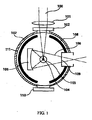
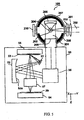
- FIG. 1 A first representative embodiment of an X-ray generator is depicted in FIG. 1.
- the X-ray generator comprises a vacuum chamber 107 that is connected in a conventional manner to a vacuum pump (not shown) that evacuates the atmosphere inside the vacuum chamber 107 to a vacuum level of several Torr or less.
- a vacuum pump not shown
- pulsed laser light 100 can propagate to the target material without being absorbed and/or attenuated by air, and X-ray radiation produced by the plasma 104 will not be damped significantly by absorption.
- a multilayer-film, ellipsoidal focusing mirror 105 is disposed near the plasma 104.
- the reflective surface of the focusing mirror 105 is coated with multiple alternating layers of Mo and Si to form a multilayer-film interference coating.
- the period length of the multilayer film is changed as required over the reflective surface so as to achieve maximal EUV reflectivity at all points on the reflective surface.
- the rear of the focusing mirror 105 is cooled by a cooling mechanism (not shown but well understood in the art).
- EUV light 106 reflected by the mirror 105 passes through a filter 109 that blocks infrared, visible, and ultraviolet light and transmits EUV radiation of a particular wavelength.
- EUV radiation passing through the filter enters a downstream illumination-optical system (not shown, but see FIG. 5, discussed later below).
- the infrared, visible, and ultraviolet wavelengths that are blocked by the filter 109 are generated by the plasma 104 but otherwise would adversely affect the resolution of fine pattern elements.
- the filter 109 only transmits the required wavelength of EUV light.
- the inner walls of the vacuum chamber 107 are lined with a film 108 of carbon black.
- Carbon black is highly absorptive to electromagnetic radiation in the range from infrared to X-ray. "Highly absorptive" in this context means that the subject material absorbs at least 90% of the incident radiation in the range of infrared through ultraviolet. (Absorption of untreated metals to these wavelengths typically is less than several percent.) Consequently, the carbon black film 108 prevents components such as the mirror 105 from being heated by reflected and/or scattered infrared to X-ray radiation from the inner walls of the vacuum chamber 107.
- a cooling jacket 111 can be fitted to the exterior, for example, of the vacuum chamber 107.
- Various materials, other than carbon black, that are highly absorptive to electromagnetic radiation ranging from infrared to X-ray alternatively can be used.
- Exemplary alternative materials include benzene soot, fullerenc, carbon nanotubes, and Aquadag® (an aqueous colloidal suspension of graphite made by, e.g. , Macalaster Bicknell).
- Benzene soot is a soot produced by burning benzene.
- any of various porous materials may be used for absorbing incident electromagnetic radiation ranging from infrared to X-ray. Porous materials have innumerable microscopic holes in their surfaces.
- the carbon black coating 108 can be formed by applying carbon black to the inner walls of the vacuum chamber 107.
- the inner walls themselves can be modified (without application of a substance to them) so as to confer to the inner walls a high absorptivity to electromagnetic radiation ranging from infrared to X-ray.
- the inner walls of an aluminum vacuum chamber 107 can be blackened by anodizing or attaching a unit of anodized aluminum.
- plates or sheets of a material that is highly absorptive to electromagnetic radiation ranging from infrared to X-ray can be adhered to the inner walls of the vacuum chamber 107.
- plates or sheets of carbon (as a representative black material) or plates or sheets of porous silicon (as a representative porous material) may be adhered conformably to the inner walls of the vacuum chamber 107.
- a porous material is used for lining the inner walls, as discussed above, a high vacuum inside the vacuum chamber 107 probably will not be attainable. However, no problem is posed by an inability to achieve high vacuum so long as the actually attainable vacuum level is sufficient for generating a plasma in the X-ray source and for propagating the EUV light 106 produced by the source.
- a vacuum level suitable for meeting these criteria is several tenths of a Torr to several Torr. This range is achievable in a chamber lined with a porous material.
- Porous material can be applied or adhered to the entire surfaces of the inner walls of the vacuum chamber. Alternatively, the material can be applied or adhered only to those portions of the inner walls at which radiation from the plasma 104 will be incident, or from which heat-producing reflection will occur.
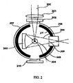
- FIG. 2 A second representative embodiment of an X-ray generator is depicted in FIG. 2.
- the depicted X-ray generator comprises a vacuum chamber 207, a lens 201 and first window 202 that pass a beam 200 of pulsed laser light, a gas-jet nozzle 203 at which a plasma 204 is formed, an ellipsoidal mirror 205 that produces a reflected beam 206, a filter 209 through which the reflected beam 206 passes, and a second window 210.
- These components are similar to corresponding components in the embodiment of FIG. 1.
- the X-ray generator of FIG. 2 differs from the embodiment of FIG. 1 mainly in that the embodiment of FIG.
- the 2 comprises a brushy layer 208 of multiple needle-shaped members 211, rather than the film 108 in the FIG.-1 embodiment, disposed on the inside wall of the vacuum chamber 207.
- the tips of the needle-shaped members 211 desirably are oriented toward the plasma 204
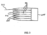
- FIG. 3 Enlarged detail of several needle-shaped members 211 is shown in FIG. 3.
- Light 212 radiating from the plasma 204 is incident on respective tapered surfaces 213 of tips 214 of the needle-shaped members 208, from which tapered surfaces the incident light is reflected multiple times toward the bulk mass of the brushy layer 208.
- the incident light ultimately is absorbed by the brushy layer 208, which can absorb light in a broad wavelength band ranging from infrared to X-ray.
- the brushy layer 208 behaves as a nearly ideal black body.
- the material used for fabricating the brushy layer 208 can be metal ( e.g. , stainless steel or aluminum), glass, carbon, organic material ( e.g. , organic polymer), or silane material ( e.g. , silicone polymer).
- the needle-shaped members 211 in FIGS. 2 and 3 appear in the figures as having sharp tips 214. This depicted configuration is not intended to be limiting because the tips of individual needle-shaped members 211 need not be “sharp” so long as the brushy layer 208 functions in the manner described above.
- the members 211 can be bristle-shaped or blade-shaped.
- the brushy layer 208 can be a "carpet" of glass fibers, carbon fibers, metal fibers or bristles, or an array of blade-shaped members.
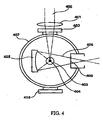
- the vacuum chamber 407 can be made of a material, other than quartz glass, exhibiting high transmissivity to light in the range of infrared to ultraviolet.
- Exemplary materials in this regard are conventional glass, magnesium fluoride (MgF 2 ), and calcium fluoride (CaF 2 ).
- the inner walls and/or the outer walls of the vacuum chamber 407 may be coated with an antireflective coating. Such a coating further decreases the amount of light 406 reflected from the walls of the chamber.
- the vacuum chamber 407 may be made entirely of quartz glass. Alternatively, portions of the chamber requiring greater mechanical strength than provided by quartz glass may be formed of metal bonded to the quartz glass used for making the rest of the chamber.
- the respective X-ray generators were described as comprising laser-plasma X-ray (LPX) sources. It will be understood that individual X-ray generators alternatively can be another type of plasma X-ray source, such as a discharge-plasma X-ray source.
- LPX laser-plasma X-ray
- FIG. 5 An embodiment of a microlithography system incorporating an X-ray generator 199 as described above is shown in FIG. 5.
- the X-ray generator 199 included with the depicted system is configured according to the embodiment shown in FIG. 2.
- the X-ray generator 199 is disposed on "top" of an exposure chamber 50.
- the exposure chamber 50 contains an illumination-optical system 56 that receives an EUV beam 206 reflected from the mirror 205 of the X-ray generator 199.
- the illumination-optical system 56 comprises one or more condenser mirrors and at least one fly-eye optical system (or analogous feature).
- the beam of EUV light reflected from the mirror 205 is directed as an "illumination beam" to the left (in the figure) by the illumination-optical system 56.
- FIG. 5 only parallel rays of light propagating to the illumination-optical system 56 are shown.
- a vertically mounted reflective mirror 52 receives the illumination beam from the illumination-optical system 56.
- the mirror 52 is circular with a concave reflective surface 52a facing right in FIG. 5.
- Light of the illumination beam reflected from the mirror 52 is reflected by a light-path-bending mirror 51 toward a reflective reticle 53.
- the reticle 53 is horizontally mounted with its EUV-reflective surface facing downward in FIG. 5.
- the mirror 52 focuses the illumination beam, propagating from the illumination-optical system 56 and reflected by the mirror 51, onto the reflective surface of the reticle 53.
- Each of the mirrors 51, 52 is made from a respective mirror substrate (e.g. , quartz) that has been finely machined to form an extremely accurate reflection surface (e.g. , item 52a in FIG. 5).
- a respective multilayer-film coating e.g. , a Mo/Si multilayer-film coating for reflecting EUV radiation of approximately 13-nm wavelength
- the multilayer-film can be formed of other substances such as Ru or Rh as the "high-Z” layer and Si, Be, or B 4 C as the "low-Z” layer.
- a multilayer-film coating also is formed on the reflective surface of the reticle 53.
- Formed on the multilayer film of the reticle 53 is an "absorbing-body" layer that is patterned into individual absorbing bodies that, together with spaces between the absorbing bodies, define a reticle pattern to be transfer-exposed from the reticle 53 to a lithographic substrate 59 ( e.g. , resist-coated semiconductor wafer).
- the reticle 53 is mounted to a reticle stage 55 that is movable in at least the Y direction.
- the illumination beam, shaped by the illumination-optical system 56 and reflected by the bending mirror 51, is illuminated on successive regions of the reticle 53 in a sequential manner, as effected by movements of the reticle stage 55.
- EUV light reflected from the reticle 53 constitutes a "patterned beam” that carries an aerial image of the pattern portion in the respective illuminated portion of the reticle 53.
- the exposure chamber 50 also contains a projection-optical system 57 and the substrate 59 situated downstream of the reticle 53.
- the projection-optical system 57 comprises multiple mirrors that demagnify the aerial image carried by the patterned beam by a specified "reduction" factor (e.g. , 1/4) and form the corresponding actual image on the substrate 59.
- the substrate 59 is mounted to a substrate stage 54 that is movable in the X, Y, and Z directions.
- the illumination beam is directed by the illumination-optical system 56 onto the reflective surface of the reticle 53.
- the reticle 53 and substrate 59 are synchronously moved in a scanning manner relative to each other and with respect to the projection-optical system 57 at a specified velocity ratio determined by the reduction factor of the projection-optical system.
- the pattern defined on the reticle 53 is transferred to one or more respective dies on the substrate 59.
- Individual dies ("chips”) on the substrate 59 have dimensions of, for example, 25 mm ⁇ 25 mm, and the pattern is formed on the substrate 59 with a line-and-space (L/S) resolution of at least 0.07 ⁇ m.
- L/S line-and-space
Landscapes
- Physics & Mathematics (AREA)
- General Physics & Mathematics (AREA)
- Engineering & Computer Science (AREA)
- Optics & Photonics (AREA)
- Plasma & Fusion (AREA)
- Exposure Of Semiconductors, Excluding Electron Or Ion Beam Exposure (AREA)
- Exposure And Positioning Against Photoresist Photosensitive Materials (AREA)
- X-Ray Techniques (AREA)
Abstract
Description
Claims (19)
- An X-ray generator, comprising:an X-ray source in which a plasma is produced from a target material and X-rays are emitted from the plasma; anda vacuum chamber defined by walls and containing the X-ray source, the walls including respective inner surfaces configured so that at least a portion of the inner surfaces absorbs incident electromagnetic radiation, produced by the plasma, in a wavelength range from infrared to X-ray radiation, the portion representing a location from which the electromagnetic radiation otherwise would reflect back into the vacuum chamber and heat a component situated inside the vacuum chamber.
- An X-ray generator according to Claim 1, wherein the X-ray source is a laser-plasma X-ray source.
- An X-ray generator according to Claim 1, wherein the X-ray source is a discharge-plasma X-ray source.
- An X-ray generator according to any preceding claim, wherein the portion of the inner surfaces is coated with carbon.
- An X-ray generator according to Claim 4, wherein the carbon is selected from the group consisting of carbon black, benzene soot, fullerene, carbon nanotubes, and dried suspensions of colloidal graphite
- An X-ray generator according to any one of Claims 1 to 3, wherein the portion of the inner surfaces comprises a porous material.
- An X-ray generator according to Claim 6, wherein the porous material is selected from the group consisting of activated charcoal and porous silicon.
- An X-ray generator according to any one of Claims 1 to 3, wherein the portion of the inner surfaces comprises anodized aluminum.
- An X-ray generator, wherein the portion of the inner surfaces comprises a brushy layer.
- An X-ray generator according to Claim 9, wherein the brushy layer comprises multiple needle-shaped members extending from the inner wall toward the plasma.
- An X-ray generator according to Claim 10, wherein the needles have respective tapered tips extending toward the plasma.
- An X-ray generator according to Claim 9, wherein the brushy layer comprises multiple bristle-shaped or blade-shaped members.
- An X-ray generator according to Claim 9, wherein the brushy layer is a carpet of glass fibres or bristles, carbon fibres or bristles, metal fibres or bristles, or silicon fibres or bristles, or combinations thereof.
- An X-ray generator according to any preceding claim, further comprising a cooling mechanism for cooling the vacuum chamber.
- An X-ray generator, comprising:an X-ray source in which a plasma is produced from a target material and X-rays are emitted from the plasma; anda vacuum chamber defined by walls and containing the X-ray source, at least a portion of the walls being made of a material that is transmissive to incident electromagnetic radiation, from the plasma, in a wavelength range from infrared to ultraviolet, the portion representing a location from which the electromagnetic radiation otherwise would reflect back into the vacuum chamber and heat a component situated inside the vacuum chamber.
- An X-ray generator according to Claim 15, wherein the portion is made of a glass material selected from the group consisting of conventional glass, quartz glass, MgF2, and CaF2.
- An X-ray generator according to Claim 15 or 16, wherein the portion includes an anti-reflective coating applied to the glass material.
- An X-ray generator, comprising:an X-ray source in which a plasma is produced from a target material and X-rays are emitted from the plasma; anda vacuum chamber defined by walls and containing the X-ray source, at least a portion of the walls being made of a material that is substantially ureflective to incident electromagnetic radiation, from the plasma, in a wavelength range from infrared to ultraviolet, the portion representing a location from which the electromagnetic radiation otherwise would reflect back into the vacuum chamber and heat a component situated inside the vacuum chamber.
- An X-ray microlithography system, comprising:an X-ray generator according to any preceding claim;an illumination-optical system situated and configured to direct an X-ray illumination beam from the X-ray generator onto a pattern-defining reticle, thereby forming a patterned beam carrying an aerial image of the pattern; anda projection-optical system situated and configured to project the patterned beam from the reticle to form an image on a sensitive substrate.
Applications Claiming Priority (2)
| Application Number | Priority Date | Filing Date | Title |
|---|---|---|---|
| JP2002026540 | 2002-02-04 | ||
| JP2002026540A JP4320999B2 (en) | 2002-02-04 | 2002-02-04 | X-ray generator and exposure apparatus |
Publications (2)
| Publication Number | Publication Date |
|---|---|
| EP1335640A2 true EP1335640A2 (en) | 2003-08-13 |
| EP1335640A3 EP1335640A3 (en) | 2007-02-21 |
Family
ID=27606472
Family Applications (1)
| Application Number | Title | Priority Date | Filing Date |
|---|---|---|---|
| EP03002336A Withdrawn EP1335640A3 (en) | 2002-02-04 | 2003-02-03 | Plasma-type X-ray source encased in vacuum chamber exhibiting reduced heating of interior components, and microlithography systems comprising same |
Country Status (3)
| Country | Link |
|---|---|
| US (1) | US20030147499A1 (en) |
| EP (1) | EP1335640A3 (en) |
| JP (1) | JP4320999B2 (en) |
Cited By (8)
| Publication number | Priority date | Publication date | Assignee | Title |
|---|---|---|---|---|
| WO2015074859A1 (en) * | 2013-11-25 | 2015-05-28 | Asml Netherlands B.V. | An apparatus, a device and a device manufacturing method |
| WO2015175760A1 (en) * | 2014-05-15 | 2015-11-19 | Excelitas Technologies Corp. | Laser driven sealed beam lamp |
| US9576785B2 (en) | 2015-05-14 | 2017-02-21 | Excelitas Technologies Corp. | Electrodeless single CW laser driven xenon lamp |
| US9741553B2 (en) | 2014-05-15 | 2017-08-22 | Excelitas Technologies Corp. | Elliptical and dual parabolic laser driven sealed beam lamps |
| US10008378B2 (en) | 2015-05-14 | 2018-06-26 | Excelitas Technologies Corp. | Laser driven sealed beam lamp with improved stability |
| US10057973B2 (en) | 2015-05-14 | 2018-08-21 | Excelitas Technologies Corp. | Electrodeless single low power CW laser driven plasma lamp |
| US10109473B1 (en) | 2018-01-26 | 2018-10-23 | Excelitas Technologies Corp. | Mechanically sealed tube for laser sustained plasma lamp and production method for same |
| US10186416B2 (en) | 2014-05-15 | 2019-01-22 | Excelitas Technologies Corp. | Apparatus and a method for operating a variable pressure sealed beam lamp |
Families Citing this family (32)
| Publication number | Priority date | Publication date | Assignee | Title |
|---|---|---|---|---|
| US7087914B2 (en) * | 2004-03-17 | 2006-08-08 | Cymer, Inc | High repetition rate laser produced plasma EUV light source |
| US7250620B2 (en) * | 2005-01-20 | 2007-07-31 | Infineon Technologies Ag | EUV lithography filter |
| ITVE20050037A1 (en) * | 2005-08-04 | 2007-02-05 | Marco Sumini | EQUIPMENT FOR RADIOTHERAPY OF INTERSTIAL AND INTRAOPERATIVE RADIOTHERAPY. |
| JP2007107075A (en) * | 2005-10-17 | 2007-04-26 | Nippon Telegr & Teleph Corp <Ntt> | Manufacturing method of oxide superconductor thin film |
| US8525138B2 (en) | 2006-03-31 | 2013-09-03 | Energetiq Technology, Inc. | Laser-driven light source |
| JP2007294673A (en) * | 2006-04-25 | 2007-11-08 | Nikon Corp | Exposure equipment |
| JP5034362B2 (en) * | 2006-08-08 | 2012-09-26 | ウシオ電機株式会社 | Extreme ultraviolet light source device |
| JP4884152B2 (en) | 2006-09-27 | 2012-02-29 | 株式会社小松製作所 | Extreme ultraviolet light source device |
| US7655925B2 (en) | 2007-08-31 | 2010-02-02 | Cymer, Inc. | Gas management system for a laser-produced-plasma EUV light source |
| EP2169464A1 (en) * | 2008-09-29 | 2010-03-31 | Carl Zeiss SMT AG | Illumination system of a microlithographic projection exposure apparatus |
| JP5314433B2 (en) | 2009-01-06 | 2013-10-16 | ギガフォトン株式会社 | Extreme ultraviolet light source device |
| JP5312959B2 (en) | 2009-01-09 | 2013-10-09 | ギガフォトン株式会社 | Extreme ultraviolet light source device |
| JP5252586B2 (en) | 2009-04-15 | 2013-07-31 | ウシオ電機株式会社 | Laser drive light source |
| DE102009043824A1 (en) * | 2009-08-21 | 2011-02-24 | Asml Netherlands B.V. | Reflective optical element and method for its production |
| US8368039B2 (en) * | 2010-04-05 | 2013-02-05 | Cymer, Inc. | EUV light source glint reduction system |
| EP2533078B1 (en) * | 2011-06-09 | 2014-02-12 | ASML Netherlands BV | Radiation source and lithographic apparatus |
| JP5839672B2 (en) * | 2011-09-28 | 2016-01-06 | 株式会社日立製作所 | Low vacuum soft X-ray experimental equipment |
| JP6189041B2 (en) | 2013-02-06 | 2017-08-30 | ギガフォトン株式会社 | Chamber and extreme ultraviolet light generator |
| US8901523B1 (en) * | 2013-09-04 | 2014-12-02 | Asml Netherlands B.V. | Apparatus for protecting EUV optical elements |
| IL234729B (en) | 2013-09-20 | 2021-02-28 | Asml Netherlands Bv | Laser-operated light source and method including mode scrambler |
| IL234727B (en) | 2013-09-20 | 2020-09-30 | Asml Netherlands Bv | Laser-operated light source in an optical system corrected for aberrations and method of designing the optical system |
| NL2013809A (en) | 2013-12-13 | 2015-06-16 | Asml Netherlands Bv | Radiation source, metrology apparatus, lithographic system and device manufacturing method. |
| WO2015086259A1 (en) | 2013-12-13 | 2015-06-18 | Asml Netherlands B.V. | Radiation source, metrology apparatus, lithographic system and device manufacturing method |
| EP3340856B1 (en) * | 2015-08-24 | 2025-07-30 | The Board of Trustees of the University of Illinois | Pixelated full-field multi-protocol stimulus source apparatus, method and system for probing visual pathway function |
| DE102016213830B3 (en) * | 2016-07-27 | 2017-12-07 | Carl Zeiss Smt Gmbh | Source hollow body and EUV plasma light source with such a hollow source body |
| US11862922B2 (en) * | 2020-12-21 | 2024-01-02 | Energetiq Technology, Inc. | Light emitting sealed body and light source device |
| EP4281824A4 (en) | 2021-01-21 | 2025-01-01 | Hamamatsu Photonics K.K. | Spectrally shaped light source |
| US11587781B2 (en) | 2021-05-24 | 2023-02-21 | Hamamatsu Photonics K.K. | Laser-driven light source with electrodeless ignition |
| US12165856B2 (en) | 2022-02-21 | 2024-12-10 | Hamamatsu Photonics K.K. | Inductively coupled plasma light source |
| US12144072B2 (en) | 2022-03-29 | 2024-11-12 | Hamamatsu Photonics K.K. | All-optical laser-driven light source with electrodeless ignition |
| US12156322B2 (en) | 2022-12-08 | 2024-11-26 | Hamamatsu Photonics K.K. | Inductively coupled plasma light source with switched power supply |
| US12578076B2 (en) | 2023-06-05 | 2026-03-17 | Hamamatsu Photonics K.K. | Dual-output laser-driven light source |
Family Cites Families (12)
| Publication number | Priority date | Publication date | Assignee | Title |
|---|---|---|---|---|
| EP0186491B1 (en) * | 1984-12-26 | 1992-06-17 | Kabushiki Kaisha Toshiba | Apparatus for producing soft x-rays using a high energy beam |
| JP3580879B2 (en) * | 1995-01-19 | 2004-10-27 | 浜松ホトニクス株式会社 | Electron tube device |
| US5963616A (en) * | 1997-03-11 | 1999-10-05 | University Of Central Florida | Configurations, materials and wavelengths for EUV lithium plasma discharge lamps |
| WO1999063790A1 (en) * | 1998-05-29 | 1999-12-09 | Nikon Corporation | Laser-excited plasma light source, exposure apparatus and its manufacturing method, and device manufacturing method |
| US6324255B1 (en) * | 1998-08-13 | 2001-11-27 | Nikon Technologies, Inc. | X-ray irradiation apparatus and x-ray exposure apparatus |
| US6285743B1 (en) * | 1998-09-14 | 2001-09-04 | Nikon Corporation | Method and apparatus for soft X-ray generation |
| JP4374735B2 (en) * | 1999-08-11 | 2009-12-02 | 株式会社ニコン | Reflective soft X-ray microscope, mask inspection apparatus, and reflective mask manufacturing method |
| JP2001110709A (en) * | 1999-10-08 | 2001-04-20 | Nikon Corp | Multilayer reflector, exposure apparatus, and integrated circuit manufacturing method. |
| TW502559B (en) * | 1999-12-24 | 2002-09-11 | Koninkl Philips Electronics Nv | Method of generating extremely short-wave radiation, method of manufacturing a device by means of said radiation, extremely short-wave radiation source unit and lithographic projection apparatus provided with such a radiation source unit |
| US6320937B1 (en) * | 2000-04-24 | 2001-11-20 | Takayasu Mochizuki | Method and apparatus for continuously generating laser plasma X-rays by the use of a cryogenic target |
| DE10048833C2 (en) * | 2000-09-29 | 2002-08-08 | Siemens Ag | Vacuum housing for a vacuum tube with an X-ray window |
| US6654446B2 (en) * | 2001-09-18 | 2003-11-25 | Euv Llc | Capillary discharge source |
-
2002
- 2002-02-04 JP JP2002026540A patent/JP4320999B2/en not_active Expired - Lifetime
-
2003
- 2003-02-03 EP EP03002336A patent/EP1335640A3/en not_active Withdrawn
- 2003-02-03 US US10/357,537 patent/US20030147499A1/en not_active Abandoned
Cited By (16)
| Publication number | Priority date | Publication date | Assignee | Title |
|---|---|---|---|---|
| US9778574B2 (en) | 2013-11-25 | 2017-10-03 | Asml Netherlands B.V. | Apparatus, a device and a device manufacturing method |
| KR102304261B1 (en) | 2013-11-25 | 2021-09-24 | 에이에스엠엘 네델란즈 비.브이. | An apparatus, a device and a device manufacturing method |
| KR20160091979A (en) * | 2013-11-25 | 2016-08-03 | 에이에스엠엘 네델란즈 비.브이. | An apparatus, a device and a device manufacturing method |
| WO2015074859A1 (en) * | 2013-11-25 | 2015-05-28 | Asml Netherlands B.V. | An apparatus, a device and a device manufacturing method |
| US10186414B2 (en) | 2014-05-15 | 2019-01-22 | Excelitas Technologies Corp. | Dual parabolic laser driven sealed beam lamps |
| US9748086B2 (en) | 2014-05-15 | 2017-08-29 | Excelitas Technologies Corp. | Laser driven sealed beam lamp |
| US9741553B2 (en) | 2014-05-15 | 2017-08-22 | Excelitas Technologies Corp. | Elliptical and dual parabolic laser driven sealed beam lamps |
| US9922814B2 (en) | 2014-05-15 | 2018-03-20 | Excelitas Technologies Corp. | Apparatus and a method for operating a sealed beam lamp containing an ionizable medium |
| US10186416B2 (en) | 2014-05-15 | 2019-01-22 | Excelitas Technologies Corp. | Apparatus and a method for operating a variable pressure sealed beam lamp |
| US10504714B2 (en) | 2014-05-15 | 2019-12-10 | Excelitas Technologies Corp. | Dual parabolic laser driven sealed beam lamp |
| WO2015175760A1 (en) * | 2014-05-15 | 2015-11-19 | Excelitas Technologies Corp. | Laser driven sealed beam lamp |
| US10008378B2 (en) | 2015-05-14 | 2018-06-26 | Excelitas Technologies Corp. | Laser driven sealed beam lamp with improved stability |
| US10057973B2 (en) | 2015-05-14 | 2018-08-21 | Excelitas Technologies Corp. | Electrodeless single low power CW laser driven plasma lamp |
| US9576785B2 (en) | 2015-05-14 | 2017-02-21 | Excelitas Technologies Corp. | Electrodeless single CW laser driven xenon lamp |
| US10497555B2 (en) | 2015-05-14 | 2019-12-03 | Excelitas Technologies Corp. | Laser driven sealed beam lamp with improved stability |
| US10109473B1 (en) | 2018-01-26 | 2018-10-23 | Excelitas Technologies Corp. | Mechanically sealed tube for laser sustained plasma lamp and production method for same |
Also Published As
| Publication number | Publication date |
|---|---|
| JP2003229298A (en) | 2003-08-15 |
| US20030147499A1 (en) | 2003-08-07 |
| JP4320999B2 (en) | 2009-08-26 |
| EP1335640A3 (en) | 2007-02-21 |
Similar Documents
| Publication | Publication Date | Title |
|---|---|---|
| US20030147499A1 (en) | Plasma-type X-ray generators encased in vacuum chambers exhibiting reduced heating of interior components, and microlithography systems comprising same | |
| JP5878120B2 (en) | EUV radiation system and lithographic apparatus | |
| KR100588113B1 (en) | Radiation source for use in lithographic projection apparatus | |
| KR101357231B1 (en) | Lpp euv light source and method for producing same | |
| KR101572930B1 (en) | Radiation system, radiation collector, radiation beam conditioning system, spectral purity filter for a radiation system and method of forming a spectral purity filter | |
| RU2249840C2 (en) | Lithographic device | |
| JP5694784B2 (en) | Light source condensing module with GIC mirror and LPP / EUV light source | |
| JP5740106B2 (en) | EUV radiation generator | |
| US8368040B2 (en) | Radiation system and lithographic apparatus | |
| US12167525B2 (en) | EUV light source and apparatus for lithography | |
| US9678432B2 (en) | Optical assembly for increasing the etendue | |
| JP6116128B2 (en) | Lithographic apparatus and method | |
| TW201639417A (en) | Extreme ultraviolet ray source module, extreme ultraviolet lithography system and extreme ultraviolet lithography process method | |
| JP2013538433A (en) | Lithographic apparatus and spectral purity filter | |
| JP2003518729A (en) | Method for generating ultrashort radiation, method for manufacturing an apparatus with said radiation, ultrashort radiation source device and lithographic projection apparatus equipped with such a radiation source device | |
| JP2014510404A (en) | System and method for cleaning an optical system in an EUV light source | |
| WO2011069881A1 (en) | Euv light source for an illumination system of a microlithographic projection exposure apparatus | |
| TW201418903A (en) | Method and apparatus for generating radiation | |
| US20140253894A1 (en) | Radiation Source | |
| TWI510821B (en) | Spectral purity filter | |
| Hansson et al. | Status of the liquid-xenon-jet laser-plasma source for EUV lithography | |
| KR20110026463A (en) | Multilayer Mirror and Lithography Equipment | |
| JP2006140470A (en) | Radiation system, lithography device, manufacturing method for device, and device manufactured by them |
Legal Events
| Date | Code | Title | Description |
|---|---|---|---|
| PUAI | Public reference made under article 153(3) epc to a published international application that has entered the european phase |
Free format text: ORIGINAL CODE: 0009012 |
|
| AK | Designated contracting states |
Designated state(s): AT BE BG CH CY CZ DE DK EE ES FI FR GB GR HU IE IT LI LU MC NL PT SE SI SK TR |
|
| AX | Request for extension of the european patent |
Extension state: AL LT LV MK RO |
|
| RIN1 | Information on inventor provided before grant (corrected) |
Inventor name: KONDO, HIROYUKI,NIKON CORP. IPHQ,FUJI BLDG. 2-3 |
|
| PUAL | Search report despatched |
Free format text: ORIGINAL CODE: 0009013 |
|
| AK | Designated contracting states |
Kind code of ref document: A3 Designated state(s): AT BE BG CH CY CZ DE DK EE ES FI FR GB GR HU IE IT LI LU MC NL PT SE SI SK TR |
|
| AX | Request for extension of the european patent |
Extension state: AL LT LV MK RO |
|
| AKX | Designation fees paid |
Designated state(s): AT BE BG CH CY CZ DE DK EE ES FI FR GB GR HU IE IT LI LU MC NL PT SE SI SK TR |
|
| STAA | Information on the status of an ep patent application or granted ep patent |
Free format text: STATUS: THE APPLICATION IS DEEMED TO BE WITHDRAWN |
|
| 18D | Application deemed to be withdrawn |
Effective date: 20070822 |