EP1335219A1 - Optical waveguide diffraction grating device, method for fabricating optical waveguide diffraction grating device, multiplexing/demultiplexing module, and optical transmission system - Google Patents
Optical waveguide diffraction grating device, method for fabricating optical waveguide diffraction grating device, multiplexing/demultiplexing module, and optical transmission system Download PDFInfo
- Publication number
- EP1335219A1 EP1335219A1 EP01967755A EP01967755A EP1335219A1 EP 1335219 A1 EP1335219 A1 EP 1335219A1 EP 01967755 A EP01967755 A EP 01967755A EP 01967755 A EP01967755 A EP 01967755A EP 1335219 A1 EP1335219 A1 EP 1335219A1
- Authority
- EP
- European Patent Office
- Prior art keywords
- diffraction grating
- grating device
- light
- wavelengths
- reflection band
- Prior art date
- Legal status (The legal status is an assumption and is not a legal conclusion. Google has not performed a legal analysis and makes no representation as to the accuracy of the status listed.)
- Withdrawn
Links
Images



Classifications
-
- G—PHYSICS
- G02—OPTICS
- G02B—OPTICAL ELEMENTS, SYSTEMS OR APPARATUS
- G02B6/00—Light guides; Structural details of arrangements comprising light guides and other optical elements, e.g. couplings
- G02B6/02—Optical fibres with cladding with or without a coating
-
- G—PHYSICS
- G02—OPTICS
- G02B—OPTICAL ELEMENTS, SYSTEMS OR APPARATUS
- G02B6/00—Light guides; Structural details of arrangements comprising light guides and other optical elements, e.g. couplings
- G02B6/24—Coupling light guides
- G02B6/26—Optical coupling means
- G02B6/28—Optical coupling means having data bus means, i.e. plural waveguides interconnected and providing an inherently bidirectional system by mixing and splitting signals
- G02B6/293—Optical coupling means having data bus means, i.e. plural waveguides interconnected and providing an inherently bidirectional system by mixing and splitting signals with wavelength selective means
- G02B6/29304—Optical coupling means having data bus means, i.e. plural waveguides interconnected and providing an inherently bidirectional system by mixing and splitting signals with wavelength selective means operating by diffraction, e.g. grating
- G02B6/29316—Light guides comprising a diffractive element, e.g. grating in or on the light guide such that diffracted light is confined in the light guide
- G02B6/29317—Light guides of the optical fibre type
- G02B6/29319—With a cascade of diffractive elements or of diffraction operations
- G02B6/2932—With a cascade of diffractive elements or of diffraction operations comprising a directional router, e.g. directional coupler, circulator
-
- G—PHYSICS
- G02—OPTICS
- G02B—OPTICAL ELEMENTS, SYSTEMS OR APPARATUS
- G02B6/00—Light guides; Structural details of arrangements comprising light guides and other optical elements, e.g. couplings
- G02B6/02—Optical fibres with cladding with or without a coating
- G02B6/02057—Optical fibres with cladding with or without a coating comprising gratings
- G02B6/02076—Refractive index modulation gratings, e.g. Bragg gratings
- G02B6/02123—Refractive index modulation gratings, e.g. Bragg gratings characterised by the method of manufacture of the grating
- G02B6/02133—Refractive index modulation gratings, e.g. Bragg gratings characterised by the method of manufacture of the grating using beam interference
- G02B6/02138—Refractive index modulation gratings, e.g. Bragg gratings characterised by the method of manufacture of the grating using beam interference based on illuminating a phase mask
-
- G—PHYSICS
- G02—OPTICS
- G02B—OPTICAL ELEMENTS, SYSTEMS OR APPARATUS
- G02B6/00—Light guides; Structural details of arrangements comprising light guides and other optical elements, e.g. couplings
- G02B6/24—Coupling light guides
- G02B6/26—Optical coupling means
- G02B6/28—Optical coupling means having data bus means, i.e. plural waveguides interconnected and providing an inherently bidirectional system by mixing and splitting signals
- G02B6/293—Optical coupling means having data bus means, i.e. plural waveguides interconnected and providing an inherently bidirectional system by mixing and splitting signals with wavelength selective means
- G02B6/29331—Optical coupling means having data bus means, i.e. plural waveguides interconnected and providing an inherently bidirectional system by mixing and splitting signals with wavelength selective means operating by evanescent wave coupling
- G02B6/29332—Wavelength selective couplers, i.e. based on evanescent coupling between light guides, e.g. fused fibre couplers with transverse coupling between fibres having different propagation constant wavelength dependency
- G02B6/29334—Grating-assisted evanescent light guide couplers, i.e. comprising grating at or functionally associated with the coupling region between the light guides, e.g. with a grating positioned where light fields overlap in the coupler
-
- G—PHYSICS
- G02—OPTICS
- G02B—OPTICAL ELEMENTS, SYSTEMS OR APPARATUS
- G02B6/00—Light guides; Structural details of arrangements comprising light guides and other optical elements, e.g. couplings
- G02B6/24—Coupling light guides
- G02B6/26—Optical coupling means
- G02B6/28—Optical coupling means having data bus means, i.e. plural waveguides interconnected and providing an inherently bidirectional system by mixing and splitting signals
- G02B6/293—Optical coupling means having data bus means, i.e. plural waveguides interconnected and providing an inherently bidirectional system by mixing and splitting signals with wavelength selective means
- G02B6/29346—Optical coupling means having data bus means, i.e. plural waveguides interconnected and providing an inherently bidirectional system by mixing and splitting signals with wavelength selective means operating by wave or beam interference
- G02B6/2935—Mach-Zehnder configuration, i.e. comprising separate splitting and combining means
- G02B6/29352—Mach-Zehnder configuration, i.e. comprising separate splitting and combining means in a light guide
- G02B6/29353—Mach-Zehnder configuration, i.e. comprising separate splitting and combining means in a light guide with a wavelength selective element in at least one light guide interferometer arm, e.g. grating, interference filter, resonator
-
- G—PHYSICS
- G02—OPTICS
- G02B—OPTICAL ELEMENTS, SYSTEMS OR APPARATUS
- G02B6/00—Light guides; Structural details of arrangements comprising light guides and other optical elements, e.g. couplings
- G02B6/24—Coupling light guides
- G02B6/26—Optical coupling means
- G02B6/28—Optical coupling means having data bus means, i.e. plural waveguides interconnected and providing an inherently bidirectional system by mixing and splitting signals
- G02B6/293—Optical coupling means having data bus means, i.e. plural waveguides interconnected and providing an inherently bidirectional system by mixing and splitting signals with wavelength selective means
- G02B6/29379—Optical coupling means having data bus means, i.e. plural waveguides interconnected and providing an inherently bidirectional system by mixing and splitting signals with wavelength selective means characterised by the function or use of the complete device
- G02B6/2938—Optical coupling means having data bus means, i.e. plural waveguides interconnected and providing an inherently bidirectional system by mixing and splitting signals with wavelength selective means characterised by the function or use of the complete device for multiplexing or demultiplexing, i.e. combining or separating wavelengths, e.g. 1xN, NxM
-
- G—PHYSICS
- G02—OPTICS
- G02B—OPTICAL ELEMENTS, SYSTEMS OR APPARATUS
- G02B6/00—Light guides; Structural details of arrangements comprising light guides and other optical elements, e.g. couplings
- G02B6/02—Optical fibres with cladding with or without a coating
- G02B6/02057—Optical fibres with cladding with or without a coating comprising gratings
- G02B6/02076—Refractive index modulation gratings, e.g. Bragg gratings
- G02B6/0208—Refractive index modulation gratings, e.g. Bragg gratings characterised by their structure, wavelength response
- G02B6/02085—Refractive index modulation gratings, e.g. Bragg gratings characterised by their structure, wavelength response characterised by the grating profile, e.g. chirped, apodised, tilted, helical
Definitions
- the present invention relates to a diffraction grating device in which a diffraction grating based on perturbation of refractive index is formed through a predetermined range in a light guide direction in an optical waveguide, a method of producing it, a multiplexer/demultiplexer module incorporating the diffraction grating device and configured to multiplex or demultiplex light, and an optical transmission system incorporating the multiplexer/demultiplexer module and configured to perform optical transmission with multi-wavelength signal light.
- a diffraction grating device is a device in which a diffraction grating based on perturbation of refractive index is formed through a predetermined range in a light guide direction in an optical waveguide (e.g., an optical fiber), and is able to selectively reflect light within a predetermined reflection band out of light guided through the optical waveguide, by the diffraction grating.
- a multiplexer/demultiplexer module incorporating this diffraction grating device is able to multiplex' or demultiplex light by selectively reflecting light in the reflection band by the diffraction grating device and is used, for example, in WDM (Wavelength Division Multiplexing) transmission systems configured to perform optical transmission using wavelength-multiplexed signal light of multiple wavelengths.
- WDM Widelength Division Multiplexing
- N is an average effective index of refraction in the index perturbation region of the optical waveguide.
- the diffraction grating device configured to selectively reflect the lightwaves of plural wavelengths is, however, longer in total length and higher in cost, because the plurality of diffraction gratings are formed in the respective, mutually different regions in the light guide direction of the optical waveguide.
- diffraction grating devices in which a diffraction grating based on perturbation of refractive index is formed through a predetermined range in the light guide direction in an optical waveguide and in which the diffraction grating selectively reflects lightwaves of plural wavelengths out of light guided in the optical waveguide.
- Document 1 “M. Ibsen, et al., "Sine-Sampled Fiber Bragg Gratings for Identical Multiple Wavelength Operation," IEEE Photon. Technol. Lett., Vol. 10, No. 6, pp.842-844 (1998)” describes the diffraction grating device in which a profile of the index perturbation in the predetermined range is of a sinc function type.
- a multiplexer/demultiplexer module incorporating such a diffraction grating device when applied to a WDM transmission system, crosstalk can occur between the light of the wavelengths that is to be transmitted and that has actually been transmitted by the diffraction grating device and the light of the wavelengths that is to be reflected but that has been transmitted by the diffraction grating device, in the case of the difference between the wavelengths being small, so as to increase the reception error rate. Since the diffraction grating device transmits part of the light of the wavelengths to be reflected, there are power losses in the light of the wavelengths that is to be reflected and that has actually been reflected by the diffraction grating device. Likewise, since the diffraction grating device reflects part of the light of the wavelengths to be transmitted, there are also power losses in the light of the wavelengths that is to be transmitted and that has actually been transmitted by the diffraction grating device.
- the present invention has been accomplished to solve the above problem and an object of the present invention is to provide a diffraction grating device short in total length, low in cost, and excellent in the reflection and transmission characteristics, and a method of producing the diffraction grating device. Another object of the present invention is to provide a multiplexer/demultiplexer module incorporating the diffraction grating device, and an optical transmission system incorporating the multiplexer/demultiplexer module.
- a diffraction grating device is a diffraction grating device in which a diffraction grating based on perturbation of refractive index is formed through a predetermined range in a light guide direction in an optical waveguide and in which the diffraction grating selectively reflects light in a reflection band out of light guided through the optical waveguide.
- This diffraction grating device is able to lower the maximum reflectance outside the reflection band in a state in which the minimum transmittance is set low in the reflection band. Since the diffraction grating based on the perturbation of refractive index is formed in only one region in the light guide direction in the optical waveguide, the element can be constructed in a shorter total length and at lower cost.
- the standard deviation of not less than 30 nm is suitable for controlling the maximum reflectance outside the reflection band at or below -20 dB in the case of four-wave reflection.
- the standard deviation of not less than 50 nm is suitable for controlling the maximum reflectance outside the reflection band at or below -30 dB in the case of four-wave reflection and for controlling the maximum reflectance outside the reflection band at or below -20 dB in the case of eight-wave reflection.
- the standard deviation of not less than 100 nm is suitable for controlling the maximum reflectance outside the reflection band at or below -30 dB in the case of eight-wave reflection.
- a maximum amplitude of the perturbation ⁇ n all of the diffraction grating in the predetermined range is preferably not more than two thirds of that on the assumption that all the phases ⁇ k are equal.
- This configuration is suitable for controlling the maximum reflectance outside the reflection band at or below -20 dB in a state in which the minimum transmittance in the reflection band is set at or below -20 dB.
- a minimum transmittance in each of the K wavelength bands is not more than -20 dB (preferably, not more than -30 dB), and a maximum reflectance outside the reflection band is not more than -20 dB (preferably, not more than -30 dB).
- This diffraction grating device demonstrates the smaller minimum transmittance inside the reflection band, the smaller maximum reflectance outside the reflection band, and the superior reflection and transmission characteristics, as compared with the conventional diffraction grating devices.
- This production method of the diffraction grating device permits easy production of the diffraction grating device with excellent reflection and transmission characteristics.
- a multiplexer/demultiplexer module according to the present invention comprises the above-stated diffraction grating device according to the present invention, wherein the diffraction grating device selectively reflects light in the reflection band, thereby effecting multiplexing or demultiplexing of light.
- An optical transmission system according to the present invention is an optical transmission system for performing optical transmission using wavelength-multiplexed signal light of multiple wavelengths, which comprises the above-stated multiplexer/demultiplexer module according to the present invention, wherein the multiplexer/demultiplexer module multiplexes or demultiplexes the signal light of the multiple wavelengths.
- the crosstalk is little even in the case of the difference being small between reflected wavelengths and transmitted wavelengths, the reception error rate is low, and the power losses are kept small in the light of the reflected wavelengths.
- a preferred configuration is such that the minimum transmittance in each of the K wavelength bands is not more than -20 dB and the maximum reflectance outside the reflection band is not more than -20 dB.
- a preferred configuration is such that the minimum transmittance in each of the K wavelength bands is not more than -30 dB and the maximum reflectance outside the reflection band is not more than -30 dB.
- Fig. 1 is a schematic diagram of a diffraction grating device according to the present embodiment.
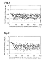
- Fig. 2 is a graph showing the relationship between the standard deviation of displacement amount and the maximum reflectance outside the reflection band in the case of four-wave reflection.
- Fig. 3 is a graph showing the relationship between the standard deviation of displacement amount and the maximum reflectance outside the reflection band in the case of eight-wave reflection.
- Figs. 4A and 4B are graphs showing the reflectance characteristics and the transmittance characteristics, respectively, of the diffraction grating device according to the present embodiment.
- Fig. 5 is a diagram to illustrate a method of producing the diffraction grating device according to the present embodiment.
- Fig. 6 is a graph showing the reflectance characteristics of the diffraction grating device in Example 1.
- Fig. 7 is a graph showing the reflectance characteristics of the diffraction grating device in Example 2.
- Fig. 8 is a graph showing the reflectance characteristics of the diffraction grating device in Comparative Example.
- Fig. 9 is a graph showing the relationship between the maximum out of maximum values of reflectance outside the reflection band and the maximum out of minimum values of transmittance in the reflection band.
- Fig. 10 is a graph showing the relationship between the maximum amplitude of the index perturbation ⁇ n all of the diffraction grating and the maximum out of maximum values of reflectance outside the reflection band.
- Fig. 11 is a schematic diagram of a multiplexer/demultiplexer module according to the first embodiment.
- Fig. 12 is a schematic diagram of a multiplexer/demultiplexer module according to the second embodiment.
- Fig. 13 is a schematic diagram of a multiplexer/demultiplexer module according to the third embodiment.
- Fig. 14 is a schematic block diagram of an optical transmission system according to the present embodiment.
- Fig. 1 is a schematic diagram of diffraction grating device 100 according to the present embodiment. This figure shows a sectional view of the diffraction grating device 100 cut by a plane including the optical axis.
- This diffraction grating device 100 is a device in which a diffraction grating 113 is formed in an optical fiber 110 as an optical waveguide.
- the optical fiber 110 contains silica glass as a principal component, a core region 111 including the center of the optical axis contains an additional component of GeO 2 , and a cladding region 112 is provided around the core region 111.
- the diffraction grating 113 based on perturbation of refractive index ⁇ n all is formed through a predetermined range in the light guide direction in the optical fiber 110.
- the perturbation of refractive index ⁇ n all (z) of this diffraction grating 113 is expressed by the equation below.
- K is an integer not less than 2
- ⁇ k represents the period of the index perturbation according to each wavelength ⁇ k to be reflected.
- ⁇ n(z) represents the amplitude of each index perturbation ⁇ n k and is represented by a super Gaussian function of a parameter z.
- the conventional diffraction grating devices encountered the problem that decrease in the minimum transmittance in the reflection band resulted in increase in the maximum reflectance outside the reflection band, while decrease in the maximum reflectance outside the reflection band resulted in increase in the minimum transmittance in the reflection band.
- the adjustment of both the amplitude and phase of each index perturbation has permitted decreasing both the maximum reflectance outside the reflection band and the minimum transmittance in the reflection band.
- ⁇ k ⁇ k - ⁇ 0
- the horizontal axis indicates the standard deviation of the displacement amount ⁇ z k and'the vertical axis the peak value of the maximum reflectance outside the reflection band.
- the standard deviation of the displacement amount ⁇ z k needs to be not less than 30 nm in order to control the peak value of the maximum reflectance outside the reflection band at or below -20 dB and that the standard deviation of the displacement amount ⁇ z k needs to be not less than 30 nm in order to control it at or below -30 dB.
- the standard deviation of the displacement amount ⁇ z k needs to be not less than 30 nm in order to control it at or below -30 dB.
- the standard deviation of the displacement amount ⁇ z k needs to be not less than 50 nm in order to control the peak value of the maximum reflectance outside the reflection band at or below -20 dB and that the standard deviation of the displacement amount ⁇ z k needs to be not less than 100 nm in order to control it at or below -30 dB.
- the standard deviation of not less than 30 nm is suitable for controlling the maximum reflectance outside the reflection band at or below -20 dB in the case of four-wave reflection.
- the standard deviation of not less than 50 nm is suitable for controlling the maximum reflectance outside the reflection band at or below -30 dB in the case of four-wave reflection and for controlling the maximum reflectance outside the reflection band at or below -20 dB in the case of eight-wave reflection.
- the standard deviation of not less than 100 nm is suitable for controlling the maximum reflectance outside the reflection band at or below -30 dB in the case of eight-wave reflection.
- This configuration is suitable for controlling the maximum reflectance outside the reflection band at or below -20 dB in a state in which the minimum transmittance in the reflection band is set at or below -20 dB.
- Figs. 4A and 4B are graphs showing an example of the reflectance characteristics and transmittance characteristics, respectively, of the diffraction grating device 100 according to the present embodiment.
- K 4.
- the reflection band is divided into four wavelength bands including respective reflection wavelengths ⁇ 1 - ⁇ 4 .
- the minimum transmittance in each of the four wavelength bands is not more than -20 dB (more preferably, not more than -30 dB).
- the maximum reflectance outside the reflection band is not more than -20 dB (more preferably, not more than -30 dB).
- the diffraction grating device 100 Since the phase ⁇ k of each index perturbation ⁇ n k has the aforementioned relation, the diffraction grating device 100 has the smaller minimum reflectance in the reflection band, the smaller maximum reflectance outside the reflection band, and the superior reflection and transmission characteristics, as compared with the conventional elements. This diffraction grating device 100 is constructed in the short total length and at low cost, because the diffraction grating 113 based on the index perturbation ⁇ n all is formed in only one range in the light guide direction in the optical fiber 110.
- a production system 300 as shown in Fig. 5 is used for production of the diffraction grating device 100.
- This system 300 is equipped with a laser source 301, a slit 303, a mirror 305, a stage 307 provided with a driving motor 307a, a phase grating 309, and a control unit 311.
- the laser source 301 emits light to induce the perturbation of refractive index in the core region 111 of the optical fiber 110.
- An excimer laser source to emit ultraviolet laser light e.g., a KrF excimer laser source or the like
- This laser source 301 is tunable in intensity of output light.
- the slit 303 allows light impinging on an aperture 303A out of the light emitted from the laser source 301 to pass through the aperture 303A and fall on the mirror 305.
- the mirror 305 reflects the light having passed through the aperture 303A of the slit 303, to make it incident on the phase grating 309.
- This mirror 305 is arranged to be movable in the longitudinal direction of the optical fiber 110 by the stage 307 having the driving motor 307a. By moving the mirror 305 in this way, it is feasible to scan in the longitudinal direction of the optical fiber 110 with the light emitted from the laser source 301 to the phase grating 309 and make the light incident into the optical fiber.
- the phase grating 309 has projections and depressions of a definite period in a side opposite to the incidence side of the light reflected by the mirror 305 (i.e., in the side where the optical fiber is placed), and diffracts the incident light. Then the phase grating 309 forms interference fringes between +1st-order diffracted light and -1st-order diffracted light and thus forms a perturbation of refractive index according to the interference fringes in the optical waveguide region of the optical fiber 110.
- the optical fiber 110 with the index perturbation thus formed in the optical waveguide region is the diffraction grating device 100.
- the control unit 311 is comprised of a CPU, a memory storing control programs, and so on. This control unit 311 is electrically coupled to the laser source 301 and controls the intensity of the light emitted from the laser source 301. The control unit 311 is also electrically coupled to the driving motor 307a of the stage 307 and controls the position of the mirror 305.
- the optical fiber 110 in which the diffraction grating 113 is to be formed is first placed immediately below the phase grating 309.
- the optical fiber 110 has the core region 111 in the central area, and the cladding region 112 surrounding the core region 111.
- Light guided through the optical fiber 110 propagates as confined in the core region 111, and part of energy of the light also exists in the cladding region 112 in the vicinity of the core region 111.
- the optical waveguide region of the optical fiber 110 includes the core region 111 and the cladding region 112 in the vicinity of the core region 111.
- the optical fiber 110 is made of silica glass as a principal component and the optical waveguide region (at least the core region) contains an additional component of GeO 2 .
- This optical fiber 110 is next exposed, for example, to the ultraviolet laser light of the wavelength of 248 nm outputted from the KrF excimer laser source 301, through the phase mask 309 having the projections and depressions of the predetermined period. Then the refractive index is modulated in the GeO 2 -doped region according to irradiation intensities, thereby forming the index perturbation ⁇ n 1 of the predetermined period ⁇ 1 .
- the nonlinear programming is based, for example, on Simulated Annealing or the genetic algorithms. This permits easy production of the above-stated diffraction grating device with excellent reflection and transmission characteristics.
- K was set to 8 and the reflected wavelengths ⁇ 1 - ⁇ 8 were set at intervals of 0.8 nm from 1547.2 nm to 1552.8 nm.
- the parameter a appearing in the function of the amplitude ⁇ n(z) of each index perturbation ⁇ n k was 2.5 ⁇ 10 -4 and the parameter b 4 mm.
- the length of the predetermined range where the diffraction grating was formed, was 20 mm. Then the phases ⁇ 1 - ⁇ 8 in each of Example 1, Example 2, and Comparative Example were set at the values presented in the table below.
- Example 1 the phases ⁇ 1 - ⁇ 8 were those designed by nonlinear programming.
- Comparative Example all the phases ⁇ 1 - ⁇ 8 were zero. Channnel Reflected wavelength (nm) Phase(degree) Example 1
- Example 2 Comparative Example 1 1547.2 -125 145 0 2 1548.0 -50 25 0 3 1548.8 -160 105 0 4 1549.6 5 60 0 5 1550.4 45 105 0 6 1551.2 35 -120 0 7 1552.0 -95 -110 0 8 1552.8 -35 100 0
- Fig. 6 is a graph showing the reflectance characteristics of the diffraction grating device in Example 1.
- Fig. 7 is a graph showing the reflectance characteristics of the diffraction grating device in Example 2.
- Fig. 8 is a graph showing the reflectance characteristics of the diffraction grating device in Comparative Example.
- the maximum is approximately -12 dB out of maximum reflectances outside the reflection band in Comparative Example, whereas the maximum is not more than -40 dB out of maximum reflectances outside the reflection band in each of Example 1 and Example 2.
- the maximum out of minimum transmittances in the reflection band is approximately -55 dB in Comparative Example, whereas the maximum out of minimum transmittances in the reflection band is also approximately -55 dB in each of Example 1 and Example 2.
- Fig. 9 is a graph showing the relationship between the maximum out of maximum reflectances outside the reflection band and the maximum out of the minimum transmittances in the reflection band.
- marks ⁇ indicate the respective cases of Example 1 and Example 2
- mark ⁇ the case of above Comparative Example
- marks o cases of other comparative examples cases in Document 1 cited in the section of (Background Art).
- the maximum reflectance outside the reflection band is smaller in the cases of Example 1 and Example 2 (marks ⁇ ) than in the cases of the comparative examples (marks ⁇ and o).
- Fig. 10 is a graph showing the relationship between the maximum amplitude of the index perturbation ⁇ n all of the diffraction grating and the maximum out of the maximum reflectances outside the reflection band.
- marks ⁇ indicate the cases of Examples in which each phase ⁇ k was designed by nonlinear programming
- mark ⁇ the case of Comparative Example where all the phases ⁇ k were zero.
- the maximum reflectance outside the reflection band is smaller in the examples (marks o) where each phase ⁇ k was set at random, and is much smaller in Examples (marks ⁇ ) in which each phase ⁇ k was designed by nonlinear programming, than that in the case of Comparative Example (mark ⁇ ) in which all the phases ⁇ k were set zero.
- the maximum amplitude of the index perturbation ⁇ n all of the diffraction grating in each Example where each phase ⁇ k was designed by nonlinear programming (marks ⁇ ) is not more than two thirds of that in Comparative Example (mark ⁇ ) in which all the phases ⁇ k were zero.
- Embodiments of the multiplexer/demultiplexer module according to the present invention will be described.
- the multiplexer/demultiplexer module in each of the embodiments described below incorporates the diffraction grating device 100 according to the above embodiment.
- the following description will be given on the assumption that the diffraction grating device 100 reflects light of wavelengths ⁇ 2m but transmits light of wavelengths ⁇ 2m+1 .
- m is an integer between 1 and M both inclusive and the wavelengths satisfy the following relation: ⁇ 1 ⁇ ⁇ 2 ⁇ ⁇ 3 ⁇ ... ⁇ ⁇ 2M-1 ⁇ ⁇ 2M
- Fig. 11 is a schematic diagram of the multiplexer/demultiplexer module 10 according to the first embodiment.
- This multiplexer/demultiplexer module 10 is constructed in a configuration wherein an optical circulator 210 is coupled to one end of the diffraction grating device 100 and another optical circulator 220 is coupled to the other end of the diffraction grating device 100.
- the optical circulator 210 has a first port 211, a second port 212, and a third port 213 and is configured to output light entering the first port 211, from the second port 212 into the diffraction grating device 100 and output light entering the second port 212, from the third port 213.
- the optical circulator 220 has a first port 221, a second port 222, and a third port 223 and is configured to output light entering the first port 221, from the second port 222 into the diffraction grating device 100 and output light entering the second port 222, from the third port 223.
- the multiplexer/demultiplexer module 10 when the light of the wavelengths ⁇ 2m+1 enters the first port 211 of the optical circulator 210, the light of these wavelengths is outputted from the second port 212 of the optical circulator 210 into the diffraction grating device 100, travels through the diffraction grating device 100, enters the second port 222 of the optical circulator 220, and is then outputted from the third port 223 of the optical circulator 220.
- the light of the wavelengths ⁇ 2m When the light of the wavelengths ⁇ 2m enters the first port 221 of the optical circulator 220, the light of these wavelengths is outputted from the second port 222 of the optical circulator 220 into the diffraction grating device 100, is reflected by the diffraction grating device 100, enters the second port 222 of the optical circulator 220, and is outputted from the third port 223 of the optical circulator 220.
- the multiplexer/demultiplexer module 10 acts as a multiplexer in this case to multiplex the light of the wavelengths ⁇ 2m+1 entering the first port 211 of the optical circulator 210, with the light of the wavelengths ⁇ 2m entering the first port 221 of the optical circulator 220 and output the multiplexed light of the wavelengths ⁇ 1 - ⁇ 2M from the third port 223 of the optical circulator 220. If the multiplexer/demultiplexer module 10 is used only as a multiplexer, the module does not have to be equipped with the optical circulator 210.
- the light of the wavelengths ⁇ 1 - ⁇ 2M enters the first port 211 of the optical circulator 210 in the multiplexer/demultiplexer module 10, the light of these wavelengths is outputted from the second port 212 of the optical circulator 210 into the diffraction grating device 100. Then the light of the wavelengths ⁇ 2m out of these lightwaves is reflected by the diffraction grating device 100, enters the second port 212 of the optical circulator 210, and is outputted from the third port 213 of the optical circulator 210.
- the multiplexer/demultiplexer module 10 acts as a demultiplexer in this case to demultiplex the light of the wavelengths ⁇ 1 - ⁇ 2M entering the first port 211 of the optical circulator 210, output the light of the wavelengths ⁇ 2m from the third port 213 of the optical circulator 210, and output the light of the wavelengths ⁇ 2m+1 from the third port 223 of the optical circulator 220.
- the multiplexer/demultiplexer module 10 is used only as a demultiplexer, the module does not have to be equipped with the optical circulator 220.
- this multiplexer/demultiplexer module 10 also acts as an optical ADM (Add-Drop Multiplexer), while acting as a multiplexer and as a demultiplexer. Specifically, the multiplexer/demultiplexer module 10 outputs the light of the wavelengths ⁇ 2m out of the wavelengths ⁇ 1 - ⁇ 2M entering the first port 211 of the optical circulator 210, from the third port 213 of the optical circulator 210 (Drop) and inputs the light of the wavelengths ⁇ 2m carrying other information, from the first port 221 of the optical circulator 220 (Add).
- ADM Add-Drop Multiplexer
- the module multiplexes the light of the wavelengths ⁇ 2m+1 out of the wavelengths ⁇ 1 - ⁇ 2M entering the first port 211 of the optical circulator 210, with the light of the wavelengths ⁇ 2m entering the first port 221 of the optical circulator 220, and outputs the multiplexed light of the wavelengths ⁇ 1 - ⁇ 2M from the third port 223 of the optical circulator 220.
- Fig. 12 is a schematic diagram of the multiplexer/demultiplexer module 20 according to the second embodiment.
- an optical fiber 110A and an optical fiber 110B are optically coupled through each of optical couplers 114A and 114B, a diffraction grating 113A is formed in a predetermined range of the optical fiber 110A between the optical coupler 114A and the optical coupler 114B to constitute a diffraction grating device 100A, and a diffraction grating 113B is formed in a predetermined range of the optical fiber 110B between the optical coupler 114A and the optical coupler 114B to constitute a diffraction grating device 100B.
- Each of these diffraction grating devices 100A and 100B is equivalent to the foregoing diffraction grating device 100.
- this multiplexer/demultiplexer module 20 when the light of the wavelengths ⁇ 2m+1 enters a first end 115A of the optical fiber 110A, the light of these wavelengths is branched by the optical coupler 114A, the branched beams travel through the respective diffraction grating devices 100A, 110B and are multiplexed by the optical coupler 114B, and the multiplexed light is outputted from a second end 116A of the optical fiber 110A.
- the light of the wavelengths ⁇ 2m enters a second end 116B of the optical fiber 110B
- the light of these wavelengths is branched by the optical coupler 114B
- the branched beams are reflected by the respective diffraction grating devices 100A, 110B and are multiplexed by the optical coupler 114B
- the multiplexed light is outputted from the second end 116A of the optical fiber 110A.
- the multiplexer/demultiplexer module 20 acts as a multiplexer in this case to multiplex the light of the wavelengths ⁇ 2m+1 entering the first end 115A of the optical fiber 110A, with the light of the wavelengths ⁇ 2m entering the second end 116B of the optical fiber 110B and output the multiplexed light of the wavelengths ⁇ 1 - ⁇ 2M from the second end 116A of the optical fiber 110A.
- the multiplexer/demultiplexer module 20 when the light of the wavelengths ⁇ 1 - ⁇ 2M enters the first end 115A of the optical fiber 110A, the light of these wavelengths is branched and outputted into the diffraction grating devices 100A, 110B by the optical coupler 114A. Then the light of the wavelengths ⁇ 2m out of these light beams is reflected by the diffraction grating devices 100A, 110B and multiplexed by the optical coupler 114A, and the multiplexed light is outputted from the first end 115B of the optical fiber 110B.
- this multiplexer/demultiplexer module 20 acts as a demultiplexer in this case to demultiplex the light of the wavelengths ⁇ 1 - ⁇ 2M entering the first end 115A of the optical fiber 110A, output the light of the wavelengths ⁇ 2m from the first end 115B of the optical fiber 110B, and output the light of the wavelengths ⁇ 2m+1 from the second end 116A of the optical fiber 110A.
- this multiplexer/demultiplexer module 20 acts both as a multiplexer and as a demultiplexer, thereby operating as an optical ADM. Namely, the multiplexer/demultiplexer module 20 operates to output the light of the wavelengths ⁇ 2m out of the wavelengths ⁇ 1 - ⁇ 2M entering the first end 115A of the optical fiber 110A, from the first end 115B of the optical fiber 110B (Drop) and input the light of the wavelengths ⁇ 2m carrying other information, from the second end 116B of the optical fiber 110B (Add).
- the module multiplexes the light of the wavelengths ⁇ 2m+1 out of the wavelengths ⁇ 1 - ⁇ 2M entering the first end 115A of the optical fiber 110A, with the light of the wavelengths ⁇ 2m entering the second end 116B of the optical fiber 110B and outputs the multiplexed light of the wavelengths ⁇ 1 - ⁇ 2M from the second end 116A of the optical fiber 110A.
- Fig. 13 is a schematic diagram of the multiplexer/demultiplexer module 30 according to the third embodiment.
- an optical fiber 110C and an optical fiber 110D are optically coupled through an optical coupler 114C, and a diffraction grating 113C is formed through a predetermined range of the coupled portion between the optical fiber 110C and the optical fiber 110D in the optical coupler 114C to constitute a diffraction grating device 100C.
- This diffraction grating device 100C is equivalent to the foregoing diffraction grating device 100. It is, however, noted that the diffraction grating 113C is formed in both the core region of the optical fiber 110C and the core region of the optical fiber 110D.
- the multiplexer/demultiplexer module 30 when the light of the wavelengths ⁇ 2m+1 enters a first end 115C of the optical fiber 110C, the light of these wavelengths travels through the diffraction grating device 100C and is outputted from a second end 116C of the optical fiber 110C.
- the light of these wavelengths When the light of the wavelengths ⁇ 2m enters a second end 116D of the optical fiber 110D, the light of these wavelengths is reflected at the diffraction grating device 100C and is outputted from the second end 116C of the optical fiber 110C.
- the multiplexer/demultiplexer module 30 acts as a multiplexer in this case to multiplex the light of the wavelengths ⁇ 2m+1 entering the first end 115C of the optical fiber 110C, with the light of the wavelengths ⁇ 2m entering the second end 116D of the optical fiber 110D and output the multiplexed light of the wavelengths ⁇ 1 - ⁇ 2M from the second end 116C of the optical fiber 110C.
- this multiplexer/demultiplexer module 30 when the light of the wavelengths ⁇ 1 - ⁇ 2M enters the first end 115C of the optical fiber 110C, the light of these wavelengths travels up to the diffraction grating device 100C. Then the light of the wavelengths ⁇ 2m out of these lightwaves is reflected by the diffraction grating device 100C to be outputted from a first end 115D of the optical fiber 110D. On the other hand, the light of the wavelengths ⁇ 2m+1 travels through the diffraction grating device 100C to be outputted from the second end 116C of the optical fiber 110C.
- the multiplexer/demultiplexer module 30 acts as a demultiplexer in this case to demultiplex the light of the wavelengths ⁇ 1 - ⁇ 2M entering the first end 115C of the optical fiber 110C, output the light of the wavelengths ⁇ 2m from the first end 115D of the optical fiber 110D, and output the light of the wavelengths ⁇ 2m+1 from the second end 116C of the optical fiber 110C.
- the multiplexer/demultiplexer module 30 also acts both as a multiplexer and as a demultiplexer, thereby operating as an optical ADM. Namely, the multiplexer/demultiplexer module 30 operates to output the light of the wavelengths ⁇ 2m out of the wavelengths ⁇ 1 - ⁇ 2M entering the first end 115C of the optical fiber 110C, from the first end 115D of the optical fiber 110D (Drop) and input the light of the wavelengths ⁇ 2m carrying other information, from the second end 116D of the optical fiber 110D (Add).
- the module multiplexes the light of the wavelengths ⁇ 2m+1 out of the light of the wavelengths ⁇ 1 - ⁇ 2M entering the first end 115C of the optical fiber 110C, with the light of the wavelengths ⁇ 2m entering the second end 116D of the optical fiber 110D and outputs the multiplexed light of the wavelengths ⁇ 1 - ⁇ 2M from the second end 116C of the optical fiber 110C.
- the multiplexer/demultiplexer modules 10, 20, and 30 described above all incorporate the diffraction grating device 100 of the present embodiment described previously, they are compact and inexpensive. Since the diffraction grating device 100 has the low transmittance in the reflection band and the low reflectance outside the reflection band, the multiplexer/demultiplexer modules 10, 20, and 30 all are resistant to occurrence of crosstalk, even in the case of the difference being small between the reflected wavelengths ⁇ 2m and the transmitted wavelengths ⁇ 2m+1 , have low reception error rates, and give rise to only small power losses in the light of the reflected wavelengths ⁇ 2m .
- Fig. 14 is a schematic block diagram of the optical transmission system 1 according to the present embodiment.
- the optical transmission system 1 is constructed in a configuration wherein an optical fiber transmission line 5 is coupled between a transmitter 2 and a repeater 3, an optical fiber transmission line 6 is also coupled between the repeater 3 and a receiver 4, and the repeater 3 is provided with the multiplexer/demultiplexer module 10.
- the transmitter 2 multiplexes signal light of the wavelengths ⁇ 1 - ⁇ 2M and sends the multiplexed light into the optical fiber transmission line 5.
- the repeater 3 receives the signal light of the wavelengths ⁇ 1 - ⁇ 2M having propagated through the optical fiber transmission line 5, demultiplexes the signal light by the multiplexer/demultiplexer module 10, sends the signal light of the wavelengths ⁇ 2m+1 into the optical fiber transmission line 6, and sends the signal light of the wavelengths ⁇ 2m into another optical fiber transmission line.
- the repeater 3 also sends signal light of the wavelengths ⁇ 2m fed through another optical fiber transmission line, into the optical fiber transmission line 6.
- the receiver 4 receives the signal light of the wavelengths ⁇ 1 - ⁇ 2M having propagated through the optical fiber transmission line 6 and demultiplexes the light of the wavelengths to complete reception.
- the optical transmission system 1 is configured to multiplex or demultiplex the signal light of the wavelengths ⁇ 1 - ⁇ 2M , using the multiplexer/demultiplexer module 10 incorporating the diffraction grating device 100 according to the present embodiment described above. Accordingly, the system is resistant to occurrence of crosstalk, even in the case of the difference being small between the reflected wavelengths ⁇ 2m and the transmitted wavelengths ⁇ 2m+1 , has a low reception error rate, and gives rise to only small power losses in the light of the reflected wavelengths ⁇ 2m .
- the multiplexer/demultiplexer module 10 may be replaced by the multiplexer/demultiplexer module 20 or 30.
- the present invention is by no means intended to be limited to the above embodiments, but the invention permits a variety of modifications.
- the diffraction grating device of the above embodiment was a device in which the diffraction grating based on the perturbation of refractive index was formed in the optical fiber as an optical waveguide.
- the element may be one in which the diffraction grating based on the perturbation of refractive index is formed in an optical waveguide formed on a flat substrate.
- the diffraction grating device has the smaller minimum transmittance in the reflection band, the smaller maximum reflectance outside the reflection band, and the superior reflection and transmission characteristics, as compared with the conventional elements.
- the diffraction grating device is short in the total length and low in cost, because the diffraction grating based on the perturbation of refractive index is formed in only one range in the light guide direction in the optical waveguide.
Landscapes
- Physics & Mathematics (AREA)
- General Physics & Mathematics (AREA)
- Optics & Photonics (AREA)
- Engineering & Computer Science (AREA)
- Manufacturing & Machinery (AREA)
- Optical Integrated Circuits (AREA)
- Diffracting Gratings Or Hologram Optical Elements (AREA)
- Optical Fibers, Optical Fiber Cores, And Optical Fiber Bundles (AREA)
Abstract
A diffraction grating device according to the
present invention is a diffraction grating device in
which a diffraction grating based on perturbation of
refractive index is formed through a predetermined
range in a light guide direction in an optical
waveguide and in which the diffraction grating
selectively reflects light in a reflection band out of
light guided through the optical waveguide. In the
diffraction grating device, the reflection band is
divided into K (K ≥ 2) wavelength bands, and the
perturbation of refractive index Δnall in the
predetermined range is represented by the sum of index
perturbations Δnk (k = 1-K) of periods Λk according to
the respective K wavelength bands. Furthermore, at
least one set of phases out of phases ϕk (k = 1-K) of
the index perturbations Δnk at a center position of the
predetermined range are different from each other.
This permits provision of the diffraction grating
device in a short total length, at low cost, and with
excellent reflection and transmission characteristics.
Description
The present invention relates to a diffraction
grating device in which a diffraction grating based on
perturbation of refractive index is formed through a
predetermined range in a light guide direction in an
optical waveguide, a method of producing it, a
multiplexer/demultiplexer module incorporating the
diffraction grating device and configured to multiplex
or demultiplex light, and an optical transmission
system incorporating the multiplexer/demultiplexer
module and configured to perform optical transmission
with multi-wavelength signal light.
A diffraction grating device is a device in which
a diffraction grating based on perturbation of
refractive index is formed through a predetermined
range in a light guide direction in an optical
waveguide (e.g., an optical fiber), and is able to
selectively reflect light within a predetermined
reflection band out of light guided through the optical
waveguide, by the diffraction grating. A
multiplexer/demultiplexer module incorporating this
diffraction grating device is able to multiplex' or
demultiplex light by selectively reflecting light in
the reflection band by the diffraction grating device
and is used, for example, in WDM (Wavelength Division
Multiplexing) transmission systems configured to
perform optical transmission using wavelength-multiplexed
signal light of multiple wavelengths.
In general, the diffraction grating device is
provided with the diffraction grating based on the
refractive index perturbation of a definite period Λ
through the predetermined range in the light guide
direction in the optical waveguide and this diffraction
grating selectively reflects light of wavelength λ
satisfying the Bragg condition represented by the
equation of λ = 2N·Λ, but transmits light of the other
wavelengths. Here N is an average effective index of
refraction in the index perturbation region of the
optical waveguide.
When a diffraction grating device is constructed
in a configuration wherein K diffraction gratings based
on refractive index perturbations of mutually different
periods Λk are formed in mutually different regions
along the light guide direction of an optical
waveguide, it is able to selectively reflect lightwaves
of respective K wavelengths λk (= 2N·Λk) (k = 1-K,
where K ≥ 2). The diffraction grating device
configured to selectively reflect the lightwaves of
plural wavelengths is, however, longer in total length
and higher in cost, because the plurality of
diffraction gratings are formed in the respective,
mutually different regions in the light guide direction
of the optical waveguide.
In contrast to it, there are the known
diffraction grating devices in which a diffraction
grating based on perturbation of refractive index is
formed through a predetermined range in the light guide
direction in an optical waveguide and in which the
diffraction grating selectively reflects lightwaves of
plural wavelengths out of light guided in the optical
waveguide. For example, Document 1 "M. Ibsen, et al.,
"Sine-Sampled Fiber Bragg Gratings for Identical
Multiple Wavelength Operation," IEEE Photon. Technol.
Lett., Vol. 10, No. 6, pp.842-844 (1998)" describes the
diffraction grating device in which a profile of the
index perturbation in the predetermined range is of a
sinc function type. Document 2 "L. A. Everall, et al.,
"Fabrication of multipassband moire resonators in
fibers by the dual-phase-mask exposure method," Opt.
Lett., Vol. 22, No. 19, pp.1473-1475 (1997)" describes
the diffraction grating device in which index
perturbations of periods Λk (k = 1-K) are
superimposedly formed in the predetermined range.
The Inventor et al. studied the above
conventional technologies and found the following
problem. Specifically, since the diffraction grating
devices described in Documents 1 and 2 above have the
diffraction grating based on the perturbation of
refractive index, formed in only one region in the
light guide direction in the optical waveguide, they
are short in total length and low in cost. However,
these diffraction grating devices still have
significant transmittance at the wavelengths λk to be
reflected, and thus transmit part of the lightwaves of
the wavelengths λk to be reflected (k = 1-K). In
addition, there exist wavelengths where the reflectance
becomes peak, outside the reflection band, and the
reflectance is high at the wavelengths; thus, part of
the light of the wavelengths to be transmitted is
reflected.
Therefore, when a multiplexer/demultiplexer
module incorporating such a diffraction grating device
is applied to a WDM transmission system, crosstalk can
occur between the light of the wavelengths that is to
be transmitted and that has actually been transmitted
by the diffraction grating device and the light of the
wavelengths that is to be reflected but that has been
transmitted by the diffraction grating device, in the
case of the difference between the wavelengths being
small, so as to increase the reception error rate.
Since the diffraction grating device transmits part of
the light of the wavelengths to be reflected, there are
power losses in the light of the wavelengths that is to
be reflected and that has actually been reflected by
the diffraction grating device. Likewise, since the
diffraction grating device reflects part of the light
of the wavelengths to be transmitted, there are also
power losses in the light of the wavelengths that is to
be transmitted and that has actually been transmitted
by the diffraction grating device.
The present invention has been accomplished to
solve the above problem and an object of the present
invention is to provide a diffraction grating device
short in total length, low in cost, and excellent in
the reflection and transmission characteristics, and a
method of producing the diffraction grating device.
Another object of the present invention is to provide a
multiplexer/demultiplexer module incorporating the
diffraction grating device, and an optical transmission
system incorporating the multiplexer/demultiplexer
module.
A diffraction grating device according to the
present invention is a diffraction grating device in
which a diffraction grating based on perturbation of
refractive index is formed through a predetermined
range in a light guide direction in an optical
waveguide and in which the diffraction grating
selectively reflects light in a reflection band out of
light guided through the optical waveguide. The
reflection band is divided into K (K ≥ 2) wavelength
bands and the perturbation of refractive index Δnall in
the predetermined range is represented by the sum of
index perturbations Δnk (k = 1-K) of periods Λk
according to the respective K wavelength bands.
Furthermore, at least one set of phases out of phases
ϕk (k = 1-K) of the index perturbations Δnk at a center
position of the predetermined range are different from
each other.
This diffraction grating device is able to lower
the maximum reflectance outside the reflection band in
a state in which the minimum transmittance is set low
in the reflection band. Since the diffraction grating
based on the perturbation of refractive index is formed
in only one region in the light guide direction in the
optical waveguide, the element can be constructed in a
shorter total length and at lower cost.
In the diffraction grating device according to
the present invention, a standard deviation of a
displacement amount Δzk = Λk·Δϕk/360 (k = 1-K), which is
expressed using a phase shift amount Δϕk (k = 1-K)
between a reference phase ϕ0 and the phase ϕk at the
center position of the predetermined range of each of
the index perturbations Δnk (k = 1-K), is preferably
not less than 30 nm, more preferably not less than 50
nm, and still more preferably not less than 100 nm.
The standard deviation of not less than 30 nm is
suitable for controlling the maximum reflectance
outside the reflection band at or below -20 dB in the
case of four-wave reflection. The standard deviation
of not less than 50 nm is suitable for controlling the
maximum reflectance outside the reflection band at or
below -30 dB in the case of four-wave reflection and
for controlling the maximum reflectance outside the
reflection band at or below -20 dB in the case of
eight-wave reflection. The standard deviation of not
less than 100 nm is suitable for controlling the
maximum reflectance outside the reflection band at or
below -30 dB in the case of eight-wave reflection.
In the diffraction grating device according to
the present invention, a maximum amplitude of the
perturbation Δnall of the diffraction grating in the
predetermined range is preferably not more than two
thirds of that on the assumption that all the phases ϕk
are equal. This configuration is suitable for
controlling the maximum reflectance outside the
reflection band at or below -20 dB in a state in which
the minimum transmittance in the reflection band is set
at or below -20 dB.
In the diffraction grating device according to
the present invention, preferably, a minimum
transmittance in each of the K wavelength bands is not
more than -20 dB (preferably, not more than -30 dB),
and a maximum reflectance outside the reflection band
is not more than -20 dB (preferably, not more than -30
dB). This diffraction grating device demonstrates the
smaller minimum transmittance inside the reflection
band, the smaller maximum reflectance outside the
reflection band, and the superior reflection and
transmission characteristics, as compared with the
conventional diffraction grating devices.
A production method of a diffraction grating
device according to the present invention is a method
of producing the above-stated diffraction grating
device according to the present invention, wherein the
phases ϕk (k = 1-K) are designed by nonlinear
programming and the diffraction grating device is
produced based thereon. This production method of the
diffraction grating device permits easy production of
the diffraction grating device with excellent
reflection and transmission characteristics.
A multiplexer/demultiplexer module according to
the present invention comprises the above-stated
diffraction grating device according to the present
invention, wherein the diffraction grating device
selectively reflects light in the reflection band,
thereby effecting multiplexing or demultiplexing of
light. An optical transmission system according to the
present invention is an optical transmission system for
performing optical transmission using wavelength-multiplexed
signal light of multiple wavelengths, which
comprises the above-stated multiplexer/demultiplexer
module according to the present invention, wherein the
multiplexer/demultiplexer module multiplexes or
demultiplexes the signal light of the multiple
wavelengths. In this configuration, the crosstalk is
little even in the case of the difference being small
between reflected wavelengths and transmitted
wavelengths, the reception error rate is low, and the
power losses are kept small in the light of the
reflected wavelengths.
For the module performing only either one of
multiplexing and demultiplexing, a preferred
configuration is such that the minimum transmittance in
each of the K wavelength bands is not more than -20 dB
and the maximum reflectance outside the reflection band
is not more than -20 dB. For the module performing
both multiplexing and demultiplexing, a preferred
configuration is such that the minimum transmittance in
each of the K wavelength bands is not more than -30 dB
and the maximum reflectance outside the reflection band
is not more than -30 dB.
The present invention can be further fully
understood from the detailed description and the
accompanying drawings which will follow. It should be
noted that these are presented merely for the
illustrative purpose, but are not to be understood in
the way to limit the present invention.
Fig. 1 is a schematic diagram of a diffraction
grating device according to the present embodiment.
Fig. 2 is a graph showing the relationship
between the standard deviation of displacement amount
and the maximum reflectance outside the reflection band
in the case of four-wave reflection.
Fig. 3 is a graph showing the relationship
between the standard deviation of displacement amount
and the maximum reflectance outside the reflection band
in the case of eight-wave reflection.
Figs. 4A and 4B are graphs showing the
reflectance characteristics and the transmittance
characteristics, respectively, of the diffraction
grating device according to the present embodiment.
Fig. 5 is a diagram to illustrate a method of
producing the diffraction grating device according to
the present embodiment.
Fig. 6 is a graph showing the reflectance
characteristics of the diffraction grating device in
Example 1.
Fig. 7 is a graph showing the reflectance
characteristics of the diffraction grating device in
Example 2.
Fig. 8 is a graph showing the reflectance
characteristics of the diffraction grating device in
Comparative Example.
Fig. 9 is a graph showing the relationship
between the maximum out of maximum values of
reflectance outside the reflection band and the maximum
out of minimum values of transmittance in the
reflection band.
Fig. 10 is a graph showing the relationship
between the maximum amplitude of the index perturbation
Δnall of the diffraction grating and the maximum out of
maximum values of reflectance outside the reflection
band.
Fig. 11 is a schematic diagram of a
multiplexer/demultiplexer module according to the first
embodiment.
Fig. 12 is a schematic diagram of a
multiplexer/demultiplexer module according to the
second embodiment.
Fig. 13 is a schematic diagram of a
multiplexer/demultiplexer module according to the third
embodiment.
Fig. 14 is a schematic block diagram of an
optical transmission system according to the present
embodiment.
Embodiments of the present invention will be
described below in detail with reference to the
accompanying drawings. In the description of the
drawings the same elements will be denoted by the same
reference symbols and redundant description will be
omitted.
First, embodiments of the diffraction grating
device and the production method thereof according to
the present invention will be described. Fig. 1 is a
schematic diagram of diffraction grating device 100
according to the present embodiment. This figure shows
a sectional view of the diffraction grating device 100
cut by a plane including the optical axis. This
diffraction grating device 100 is a device in which a
diffraction grating 113 is formed in an optical fiber
110 as an optical waveguide. The optical fiber 110
contains silica glass as a principal component, a core
region 111 including the center of the optical axis
contains an additional component of GeO2, and a
cladding region 112 is provided around the core region
111. The diffraction grating 113 based on perturbation
of refractive index Δnall is formed through a
predetermined range in the light guide direction in the
optical fiber 110.
When the z-axis is taken along the light guide
direction with the origin at the center position of the
predetermined range where the diffraction grating 113
is formed, the perturbation of refractive index Δnall(z)
of this diffraction grating 113 is expressed by the
equation below.


 Here K is an integer not less than 2, and the index
perturbation Δnall of the diffraction grating 113 is
represented by the sum of index perturbations Δnk (k =
1-K) of definite periods Λk. Λk represents the period
of the index perturbation according to each wavelength
λk to be reflected. ϕk indicates the phase at the
origin (z = 0) of the kth index perturbation Δnk.
Δn(z) represents the amplitude of each index
perturbation Δnk and is represented by a super Gaussian
function of a parameter z.
Here K is an integer not less than 2, and the index
perturbation Δnall of the diffraction grating 113 is
represented by the sum of index perturbations Δnk (k =
1-K) of definite periods Λk. Λk represents the period
of the index perturbation according to each wavelength
λk to be reflected. ϕk indicates the phase at the
origin (z = 0) of the kth index perturbation Δnk.
Δn(z) represents the amplitude of each index
perturbation Δnk and is represented by a super Gaussian
function of a parameter z.
In the diffraction grating device 100 according
to the present embodiment, at least one set of phases
out of the phases ϕk (k = 1-K) of the index
perturbations Δnk are intentionally set at different
values and thus are different from each other. This
makes it feasible to decrease the maximum reflectance
outside the reflection band in a state in which the
minimum transmittance in the reflection band is set
small. Namely, the conventional diffraction grating
devices encountered the problem that decrease in the
minimum transmittance in the reflection band resulted
in increase in the maximum reflectance outside the
reflection band, while decrease in the maximum
reflectance outside the reflection band resulted in
increase in the minimum transmittance in the reflection
band. In contrast to it, in the diffraction grating
device 100 according to the present embodiment, the
adjustment of both the amplitude and phase of each
index perturbation has permitted decreasing both the
maximum reflectance outside the reflection band and the
minimum transmittance in the reflection band.
Here a phase shift amount Δϕk (k = 1-K) between
the phase ϕk at the origin (z = 0) of each index
perturbation Δnk and a reference phase ϕ0 (ϕ0 is an
arbitrary value) is represented by the following
equation.
Δϕk = ϕk - ϕ0
There is a correlation between the phase shift
amount Δϕk (k = 1-K) and a displacement amount Δzk of
each index perturbation Δnk (k = 1-K), and the
displacement amount Δzk is represented by the following
equation.
ΔZk = Λk × Δϕk /360
Fig. 2 and Fig. 3 are graphs showing plots of the
results of a thousand calculations to calculate the
peak value of the maximum reflectance outside the
reflection band, for the diffraction grating devices
wherein the displacement amount Δzk (k = 1-K) at the
origin (z = 0) of each index perturbation Δnk is set at
random, in the respective cases of four-wave reflection
and eight-wave reflection. In Figs. 2 and 3, the
horizontal axis indicates the standard deviation of the
displacement amount Δzk and'the vertical axis the peak
value of the maximum reflectance outside the reflection
band.
As shown in Fig. 2, it is seen in the case of
four-wave reflection that the standard deviation of the
displacement amount Δzk needs to be not less than 30 nm
in order to control the peak value of the maximum
reflectance outside the reflection band at or below -20
dB and that the standard deviation of the displacement
amount Δzk needs to be not less than 30 nm in order to
control it at or below -30 dB. As shown in Fig. 3, it
is also seen in the case of eight-wave reflection that
the standard deviation of the displacement amount Δzk
needs to be not less than 50 nm in order to control the
peak value of the maximum reflectance outside the
reflection band at or below -20 dB and that the
standard deviation of the displacement amount Δzk needs
to be not less than 100 nm in order to control it at or
below -30 dB.
According to this finding, in the diffraction
grating device 100 of the present embodiment, the
standard deviation of the displacement amount Δzk (k =
1-K) is preferably not less than 30 nm, more preferably
not less than 50 nm, and still more preferably not less
than 100 nm. The standard deviation of not less than
30 nm is suitable for controlling the maximum
reflectance outside the reflection band at or below -20
dB in the case of four-wave reflection. The standard
deviation of not less than 50 nm is suitable for
controlling the maximum reflectance outside the
reflection band at or below -30 dB in the case of four-wave
reflection and for controlling the maximum
reflectance outside the reflection band at or below -20
dB in the case of eight-wave reflection. The standard
deviation of not less than 100 nm is suitable for
controlling the maximum reflectance outside the
reflection band at or below -30 dB in the case of
eight-wave reflection.
Alternatively, in the diffraction grating device
100 according to the present embodiment, it is
preferable that the maximum amplitude of the index
perturbation Δnall of the diffraction grating 113 be not
more than two thirds of that on the assumption that all
the phases ϕk (k = 1-K) are equal. This configuration
is suitable for controlling the maximum reflectance
outside the reflection band at or below -20 dB in a
state in which the minimum transmittance in the
reflection band is set at or below -20 dB.
Figs. 4A and 4B are graphs showing an example of
the reflectance characteristics and transmittance
characteristics, respectively, of the diffraction
grating device 100 according to the present embodiment.
In this example, K = 4. The reflection band is divided
into four wavelength bands including respective
reflection wavelengths λ1-λ4. The minimum transmittance
in each of the four wavelength bands is not more
than -20 dB (more preferably, not more than -30 dB).
The maximum reflectance outside the reflection band is
not more than -20 dB (more preferably, not more
than -30 dB).
In the diffraction grating device 100 as
described, when light of multiple wavelengths arrives
at the diffraction grating 113 through the core region
of the optical fiber 110, the diffraction grating 113
reflects light in the reflection band including the
wavelengths λk (= 2N·Λk) satisfying the Bragg condition
in any one of the index perturbations Δnk (k = 1-K) of
the definite periods Λk, out of the arriving light,
while the diffraction grating 113 transmits the other
light outside the reflection band. Since the phase ϕk
of each index perturbation Δnk has the aforementioned
relation, the diffraction grating device 100 has the
smaller minimum reflectance in the reflection band, the
smaller maximum reflectance outside the reflection
band, and the superior reflection and transmission
characteristics, as compared with the conventional
elements. This diffraction grating device 100 is
constructed in the short total length and at low cost,
because the diffraction grating 113 based on the index
perturbation Δnall is formed in only one range in the
light guide direction in the optical fiber 110.
Next, a production method of the diffraction
grating device 100 according to the present embodiment
will be described.
A production system 300 as shown in Fig. 5 is
used for production of the diffraction grating device
100. This system 300 is equipped with a laser source
301, a slit 303, a mirror 305, a stage 307 provided
with a driving motor 307a, a phase grating 309, and a
control unit 311.
The laser source 301 emits light to induce the
perturbation of refractive index in the core region 111
of the optical fiber 110. An excimer laser source to
emit ultraviolet laser light (e.g., a KrF excimer laser
source or the like) can be suitably applied as the
light source 301. This laser source 301 is tunable in
intensity of output light.
The slit 303 allows light impinging on an
aperture 303A out of the light emitted from the laser
source 301 to pass through the aperture 303A and fall
on the mirror 305. The mirror 305 reflects the light
having passed through the aperture 303A of the slit
303, to make it incident on the phase grating 309.
This mirror 305 is arranged to be movable in the
longitudinal direction of the optical fiber 110 by the
stage 307 having the driving motor 307a. By moving the
mirror 305 in this way, it is feasible to scan in the
longitudinal direction of the optical fiber 110 with
the light emitted from the laser source 301 to the
phase grating 309 and make the light incident into the
optical fiber.
The phase grating 309 has projections and
depressions of a definite period in a side opposite to
the incidence side of the light reflected by the mirror
305 (i.e., in the side where the optical fiber is
placed), and diffracts the incident light. Then the
phase grating 309 forms interference fringes between
+1st-order diffracted light and -1st-order diffracted
light and thus forms a perturbation of refractive index
according to the interference fringes in the optical
waveguide region of the optical fiber 110. The optical
fiber 110 with the index perturbation thus formed in
the optical waveguide region is the diffraction grating
device 100.
The control unit 311 is comprised of a CPU, a
memory storing control programs, and so on. This
control unit 311 is electrically coupled to the laser
source 301 and controls the intensity of the light
emitted from the laser source 301. The control unit
311 is also electrically coupled to the driving motor
307a of the stage 307 and controls the position of the
mirror 305.
In the production of the diffraction grating
device 100 using the above-stated system 300, the
optical fiber 110 in which the diffraction grating 113
is to be formed, is first placed immediately below the
phase grating 309. The optical fiber 110 has the core
region 111 in the central area, and the cladding region
112 surrounding the core region 111. Light guided
through the optical fiber 110 propagates as confined in
the core region 111, and part of energy of the light
also exists in the cladding region 112 in the vicinity
of the core region 111. Namely, the optical waveguide
region of the optical fiber 110 includes the core
region 111 and the cladding region 112 in the vicinity
of the core region 111. The optical fiber 110 is made
of silica glass as a principal component and the
optical waveguide region (at least the core region)
contains an additional component of GeO2.
This optical fiber 110 is next exposed, for
example, to the ultraviolet laser light of the
wavelength of 248 nm outputted from the KrF excimer
laser source 301, through the phase mask 309 having the
projections and depressions of the predetermined period.
Then the refractive index is modulated in the GeO2-doped
region according to irradiation intensities,
thereby forming the index perturbation Δn1 of the
predetermined period Λ1.
While successively replacing the phase mask 309
with another, the ultraviolet laser irradiation as
described is repeatedly carried out, thereby forming
the index perturbations Δnk of the definite periods Λk
in superimposed manner (k = 1-K). The location of the
phase mask 309 is determined in each of K ultraviolet
laser irradiations so that each phase ϕk (k =1-K) has
the aforementioned relation. More specifically, each
phase mask 309 is located based on the displacement
amount Δzk (k = 1-K) determined from Eq (3) above,
using each phase ϕk (k = 1-K). Here each phase ϕk (k =
1-K) is preferably designed by nonlinear programming.
The nonlinear programming is based, for example, on
Simulated Annealing or the genetic algorithms. This
permits easy production of the above-stated diffraction
grating device with excellent reflection and
transmission characteristics.
Specific examples of the diffraction grating
device according to the present embodiment will be
described below together with a comparative example.
In the examples, K was set to 8 and the reflected
wavelengths λ1-λ8 were set at intervals of 0.8 nm from
1547.2 nm to 1552.8 nm. The parameter a appearing in
the function of the amplitude Δn(z) of each index
perturbation Δnk was 2.5 × 10⁻⁴ and the parameter b 4
mm. The length of the predetermined range where the
diffraction grating was formed, was 20 mm. Then the
phases ϕ1-ϕ8 in each of Example 1, Example 2, and
Comparative Example were set at the values presented in
the table below. In each of Example 1 and Example 2,
the phases ϕ1-ϕ8 were those designed by nonlinear
programming. The standard deviation of the
displacement amount Δzk (k = 1-K) represented by Eq (3)
above was 104 nm in Example 1, and 141 nm in Example 2.
In Comparative Example all the phases ϕ1-ϕ8 were zero.
| Channnel | Reflected wavelength (nm) | Phase(degree) | ||
| Example 1 | Example 2 | Comparative Example | ||
| 1 | 1547.2 | -125 | 145 | 0 |
| 2 | 1548.0 | -50 | 25 | 0 |
| 3 | 1548.8 | -160 | 105 | 0 |
| 4 | 1549.6 | 5 | 60 | 0 |
| 5 | 1550.4 | 45 | 105 | 0 |
| 6 | 1551.2 | 35 | -120 | 0 |
| 7 | 1552.0 | -95 | -110 | 0 |
| 8 | 1552.8 | -35 | 100 | 0 |
Fig. 6 is a graph showing the reflectance
characteristics of the diffraction grating device in
Example 1. Fig. 7 is a graph showing the reflectance
characteristics of the diffraction grating device in
Example 2. Fig. 8 is a graph showing the reflectance
characteristics of the diffraction grating device in
Comparative Example. As apparent from these graphs,
the maximum is approximately -12 dB out of maximum
reflectances outside the reflection band in Comparative
Example, whereas the maximum is not more than -40 dB
out of maximum reflectances outside the reflection band
in each of Example 1 and Example 2. The maximum out of
minimum transmittances in the reflection band is
approximately -55 dB in Comparative Example, whereas
the maximum out of minimum transmittances in the
reflection band is also approximately -55 dB in each of
Example 1 and Example 2.
Fig. 9 is a graph showing the relationship
between the maximum out of maximum reflectances outside
the reflection band and the maximum out of the minimum
transmittances in the reflection band. In this figure,
marks □ indicate the respective cases of Example 1 and
Example 2, mark Δ the case of above Comparative
Example, and marks o cases of other comparative
examples (cases in Document 1 cited in the section of
(Background Art). As apparent from this graph, the
maximum reflectance outside the reflection band is
smaller in the cases of Example 1 and Example 2 (marks
□) than in the cases of the comparative examples (marks
Δ and o).
Fig. 10 is a graph showing the relationship
between the maximum amplitude of the index perturbation
Δnall of the diffraction grating and the maximum out of
the maximum reflectances outside the reflection band.
In this figure, marks □ indicate the cases of Examples
in which each phase ϕk was designed by nonlinear
programming, marks o cases of comparative examples in
which each phase ϕk was set at random (in a thousand
ways), and mark Δ the case of Comparative Example where
all the phases ϕk were zero. As apparent from this
graph, the maximum reflectance outside the reflection
band is smaller in the examples (marks o) where each
phase ϕk was set at random, and is much smaller in
Examples (marks □) in which each phase ϕk was designed
by nonlinear programming, than that in the case of
Comparative Example (mark Δ) in which all the phases ϕk
were set zero. The maximum amplitude of the index
perturbation Δnall of the diffraction grating in each
Example where each phase ϕk was designed by nonlinear
programming (marks □), is not more than two thirds of
that in Comparative Example (mark Δ) in which all the
phases ϕk were zero.
Embodiments of the multiplexer/demultiplexer
module according to the present invention will be
described. The multiplexer/demultiplexer module in
each of the embodiments described below incorporates
the diffraction grating device 100 according to the
above embodiment. The following description will be
given on the assumption that the diffraction grating
device 100 reflects light of wavelengths λ2m but
transmits light of wavelengths λ2m+1. It is also
assumed herein that m is an integer between 1 and M
both inclusive and the wavelengths satisfy the
following relation:
λ1 < λ2 < λ3 <...< λ2M-1 < λ2M
Fig. 11 is a schematic diagram of the
multiplexer/demultiplexer module 10 according to the
first embodiment. This multiplexer/demultiplexer
module 10 is constructed in a configuration wherein an
optical circulator 210 is coupled to one end of the
diffraction grating device 100 and another optical
circulator 220 is coupled to the other end of the
diffraction grating device 100. The optical circulator
210 has a first port 211, a second port 212, and a
third port 213 and is configured to output light
entering the first port 211, from the second port 212
into the diffraction grating device 100 and output
light entering the second port 212, from the third port
213. The optical circulator 220 has a first port 221,
a second port 222, and a third port 223 and is
configured to output light entering the first port 221,
from the second port 222 into the diffraction grating
device 100 and output light entering the second port
222, from the third port 223.
In the multiplexer/demultiplexer module 10, when
the light of the wavelengths λ2m+1 enters the first port
211 of the optical circulator 210, the light of these
wavelengths is outputted from the second port 212 of
the optical circulator 210 into the diffraction grating
device 100, travels through the diffraction grating
device 100, enters the second port 222 of the optical
circulator 220, and is then outputted from the third
port 223 of the optical circulator 220. When the light
of the wavelengths λ2m enters the first port 221 of the
optical circulator 220, the light of these wavelengths
is outputted from the second port 222 of the optical
circulator 220 into the diffraction grating device 100,
is reflected by the diffraction grating device 100,
enters the second port 222 of the optical circulator
220, and is outputted from the third port 223 of the
optical circulator 220. Namely, the
multiplexer/demultiplexer module 10 acts as a
multiplexer in this case to multiplex the light of the
wavelengths λ2m+1 entering the first port 211 of the
optical circulator 210, with the light of the
wavelengths λ2m entering the first port 221 of the
optical circulator 220 and output the multiplexed light
of the wavelengths λ1-λ2M from the third port 223 of the
optical circulator 220. If the
multiplexer/demultiplexer module 10 is used only as a
multiplexer, the module does not have to be equipped
with the optical circulator 210.
When the light of the wavelengths λ1-λ2M enters
the first port 211 of the optical circulator 210 in the
multiplexer/demultiplexer module 10, the light of these
wavelengths is outputted from the second port 212 of
the optical circulator 210 into the diffraction grating
device 100. Then the light of the wavelengths λ2m out
of these lightwaves is reflected by the diffraction
grating device 100, enters the second port 212 of the
optical circulator 210, and is outputted from the third
port 213 of the optical circulator 210. On the other
hand, the light of the wavelengths λ2m+1 travels through
the diffraction grating device 100, enters the second
port 222 of the optical circulator 220, and is then
outputted from the third port 223 of the optical
circulator 220. Namely, the multiplexer/demultiplexer
module 10 acts as a demultiplexer in this case to
demultiplex the light of the wavelengths λ1-λ2M entering
the first port 211 of the optical circulator 210,
output the light of the wavelengths λ2m from the third
port 213 of the optical circulator 210, and output the
light of the wavelengths λ2m+1 from the third port 223
of the optical circulator 220. When the
multiplexer/demultiplexer module 10 is used only as a
demultiplexer, the module does not have to be equipped
with the optical circulator 220.
Furthermore, this multiplexer/demultiplexer
module 10 also acts as an optical ADM (Add-Drop
Multiplexer), while acting as a multiplexer and as a
demultiplexer. Specifically, the
multiplexer/demultiplexer module 10 outputs the light
of the wavelengths λ2m out of the wavelengths λ1-λ2M
entering the first port 211 of the optical circulator
210, from the third port 213 of the optical circulator
210 (Drop) and inputs the light of the wavelengths λ2m
carrying other information, from the first port 221 of
the optical circulator 220 (Add). Then the module
multiplexes the light of the wavelengths λ2m+1 out of
the wavelengths λ1-λ2M entering the first port 211 of
the optical circulator 210, with the light of the
wavelengths λ2m entering the first port 221 of the
optical circulator 220, and outputs the multiplexed
light of the wavelengths λ1-λ2M from the third port 223
of the optical circulator 220.
Fig. 12 is a schematic diagram of the
multiplexer/demultiplexer module 20 according to the
second embodiment. In this multiplexer/demultiplexer
module 20, an optical fiber 110A and an optical fiber
110B are optically coupled through each of optical
couplers 114A and 114B, a diffraction grating 113A is
formed in a predetermined range of the optical fiber
110A between the optical coupler 114A and the optical
coupler 114B to constitute a diffraction grating device
100A, and a diffraction grating 113B is formed in a
predetermined range of the optical fiber 110B between
the optical coupler 114A and the optical coupler 114B
to constitute a diffraction grating device 100B. Each
of these diffraction grating devices 100A and 100B is
equivalent to the foregoing diffraction grating device
100.
In this multiplexer/demultiplexer module 20, when
the light of the wavelengths λ2m+1 enters a first end
115A of the optical fiber 110A, the light of these
wavelengths is branched by the optical coupler 114A,
the branched beams travel through the respective
diffraction grating devices 100A, 110B and are
multiplexed by the optical coupler 114B, and the
multiplexed light is outputted from a second end 116A
of the optical fiber 110A. When the light of the
wavelengths λ2m enters a second end 116B of the optical
fiber 110B, the light of these wavelengths is branched
by the optical coupler 114B, the branched beams are
reflected by the respective diffraction grating devices
100A, 110B and are multiplexed by the optical coupler
114B, and the multiplexed light is outputted from the
second end 116A of the optical fiber 110A. Namely, the
multiplexer/demultiplexer module 20 acts as a
multiplexer in this case to multiplex the light of the
wavelengths λ2m+1 entering the first end 115A of the
optical fiber 110A, with the light of the wavelengths
λ2m entering the second end 116B of the optical fiber
110B and output the multiplexed light of the
wavelengths λ1-λ2M from the second end 116A of the
optical fiber 110A.
In the multiplexer/demultiplexer module 20, when
the light of the wavelengths λ1-λ2M enters the first end
115A of the optical fiber 110A, the light of these
wavelengths is branched and outputted into the
diffraction grating devices 100A, 110B by the optical
coupler 114A. Then the light of the wavelengths λ2m out
of these light beams is reflected by the diffraction
grating devices 100A, 110B and multiplexed by the
optical coupler 114A, and the multiplexed light is
outputted from the first end 115B of the optical fiber
110B. On the other hand, the light of the wavelengths
λ2m+1 travels through the diffraction grating devices
100A, 110B and is multiplexed by the optical coupler
114B, and the multiplexed light is outputted from the
second end 116A of the optical fiber 110A. Namely,
this multiplexer/demultiplexer module 20 acts as a
demultiplexer in this case to demultiplex the light of
the wavelengths λ1-λ2M entering the first end 115A of
the optical fiber 110A, output the light of the
wavelengths λ2m from the first end 115B of the optical
fiber 110B, and output the light of the wavelengths
λ2m+1 from the second end 116A of the optical fiber
110A.
Furthermore, this multiplexer/demultiplexer
module 20 acts both as a multiplexer and as a
demultiplexer, thereby operating as an optical ADM.
Namely, the multiplexer/demultiplexer module 20
operates to output the light of the wavelengths λ2m out
of the wavelengths λ1-λ2M entering the first end 115A of
the optical fiber 110A, from the first end 115B of the
optical fiber 110B (Drop) and input the light of the
wavelengths λ2m carrying other information, from the
second end 116B of the optical fiber 110B (Add). Then
the module multiplexes the light of the wavelengths
λ2m+1 out of the wavelengths λ1-λ2M entering the first
end 115A of the optical fiber 110A, with the light of
the wavelengths λ2m entering the second end 116B of the
optical fiber 110B and outputs the multiplexed light of
the wavelengths λ1-λ2M from the second end 116A of the
optical fiber 110A.
Fig. 13 is a schematic diagram of the
multiplexer/demultiplexer module 30 according to the
third embodiment. In this multiplexer/demultiplexer
module 30, an optical fiber 110C and an optical fiber
110D are optically coupled through an optical coupler
114C, and a diffraction grating 113C is formed through
a predetermined range of the coupled portion between
the optical fiber 110C and the optical fiber 110D in
the optical coupler 114C to constitute a diffraction
grating device 100C. This diffraction grating device
100C is equivalent to the foregoing diffraction grating
device 100. It is, however, noted that the diffraction
grating 113C is formed in both the core region of the
optical fiber 110C and the core region of the optical
fiber 110D.
In the multiplexer/demultiplexer module 30, when
the light of the wavelengths λ2m+1 enters a first end
115C of the optical fiber 110C, the light of these
wavelengths travels through the diffraction grating
device 100C and is outputted from a second end 116C of
the optical fiber 110C. When the light of the
wavelengths λ2m enters a second end 116D of the optical
fiber 110D, the light of these wavelengths is reflected
at the diffraction grating device 100C and is outputted
from the second end 116C of the optical fiber 110C.
Namely, the multiplexer/demultiplexer module 30 acts as
a multiplexer in this case to multiplex the light of
the wavelengths λ2m+1 entering the first end 115C of the
optical fiber 110C, with the light of the wavelengths
λ2m entering the second end 116D of the optical fiber
110D and output the multiplexed light of the
wavelengths λ1-λ2M from the second end 116C of the
optical fiber 110C.
In this multiplexer/demultiplexer module 30, when
the light of the wavelengths λ1-λ2M enters the first end
115C of the optical fiber 110C, the light of these
wavelengths travels up to the diffraction grating
device 100C. Then the light of the wavelengths λ2m out
of these lightwaves is reflected by the diffraction
grating device 100C to be outputted from a first end
115D of the optical fiber 110D. On the other hand, the
light of the wavelengths λ2m+1 travels through the
diffraction grating device 100C to be outputted from
the second end 116C of the optical fiber 110C. Namely,
the multiplexer/demultiplexer module 30 acts as a
demultiplexer in this case to demultiplex the light of
the wavelengths λ1-λ2M entering the first end 115C of
the optical fiber 110C, output the light of the
wavelengths λ2m from the first end 115D of the optical
fiber 110D, and output the light of the wavelengths
λ2m+1 from the second end 116C of the optical fiber
110C.
Furthermore, the multiplexer/demultiplexer module
30 also acts both as a multiplexer and as a
demultiplexer, thereby operating as an optical ADM.
Namely, the multiplexer/demultiplexer module 30
operates to output the light of the wavelengths λ2m out
of the wavelengths λ1-λ2M entering the first end 115C of
the optical fiber 110C, from the first end 115D of the
optical fiber 110D (Drop) and input the light of the
wavelengths λ2m carrying other information, from the
second end 116D of the optical fiber 110D (Add). Then
the module multiplexes the light of the wavelengths
λ2m+1 out of the light of the wavelengths λ1-λ2M entering
the first end 115C of the optical fiber 110C, with the
light of the wavelengths λ2m entering the second end
116D of the optical fiber 110D and outputs the
multiplexed light of the wavelengths λ1-λ2M from the
second end 116C of the optical fiber 110C.
Since the multiplexer/demultiplexer modules 10,
20, and 30 described above all incorporate the
diffraction grating device 100 of the present
embodiment described previously, they are compact and
inexpensive. Since the diffraction grating device 100
has the low transmittance in the reflection band and
the low reflectance outside the reflection band, the
multiplexer/demultiplexer modules 10, 20, and 30 all
are resistant to occurrence of crosstalk, even in the
case of the difference being small between the
reflected wavelengths λ2m and the transmitted
wavelengths λ2m+1, have low reception error rates, and
give rise to only small power losses in the light of
the reflected wavelengths λ2m.
An embodiment of the optical transmission system
according to the present invention will be described
below. Fig. 14 is a schematic block diagram of the
optical transmission system 1 according to the present
embodiment. The optical transmission system 1 is
constructed in a configuration wherein an optical fiber
transmission line 5 is coupled between a transmitter 2
and a repeater 3, an optical fiber transmission line 6
is also coupled between the repeater 3 and a receiver
4, and the repeater 3 is provided with the
multiplexer/demultiplexer module 10.
The transmitter 2 multiplexes signal light of the
wavelengths λ1-λ2M and sends the multiplexed light into
the optical fiber transmission line 5. The repeater 3
receives the signal light of the wavelengths λ1-λ2M
having propagated through the optical fiber
transmission line 5, demultiplexes the signal light by
the multiplexer/demultiplexer module 10, sends the
signal light of the wavelengths λ2m+1 into the optical
fiber transmission line 6, and sends the signal light
of the wavelengths λ2m into another optical fiber
transmission line. The repeater 3 also sends signal
light of the wavelengths λ2m fed through another
optical fiber transmission line, into the optical fiber
transmission line 6. The receiver 4 receives the
signal light of the wavelengths λ1-λ2M having propagated
through the optical fiber transmission line 6 and
demultiplexes the light of the wavelengths to complete
reception.
The optical transmission system 1 is configured
to multiplex or demultiplex the signal light of the
wavelengths λ1-λ2M, using the multiplexer/demultiplexer
module 10 incorporating the diffraction grating device
100 according to the present embodiment described above.
Accordingly, the system is resistant to occurrence of
crosstalk, even in the case of the difference being
small between the reflected wavelengths λ2m and the
transmitted wavelengths λ2m+1, has a low reception error
rate, and gives rise to only small power losses in the
light of the reflected wavelengths λ2m. The
multiplexer/demultiplexer module 10 may be replaced by
the multiplexer/demultiplexer module 20 or 30.
The present invention is by no means intended to
be limited to the above embodiments, but the invention
permits a variety of modifications. For example, the
diffraction grating device of the above embodiment was
a device in which the diffraction grating based on the
perturbation of refractive index was formed in the
optical fiber as an optical waveguide. However,
without having to be limited to this, the element may
be one in which the diffraction grating based on the
perturbation of refractive index is formed in an
optical waveguide formed on a flat substrate.
The diffraction grating device according to the
present invention has the smaller minimum transmittance
in the reflection band, the smaller maximum reflectance
outside the reflection band, and the superior
reflection and transmission characteristics, as
compared with the conventional elements. The
diffraction grating device is short in the total length
and low in cost, because the diffraction grating based
on the perturbation of refractive index is formed in
only one range in the light guide direction in the
optical waveguide.
It is obvious that the present invention can be
modified in various forms from the above description of
the present invention. It is to be understood that
such modifications can be made in the invention without
departing from the spirit and scope of the present
invention, and all improvements obvious to those
skilled in the art should be included in the scope of
the claims which follow.
Claims (11)
- A diffraction grating device in which a diffraction grating based on perturbation of refractive index is formed through a predetermined range in a light guide direction in an optical waveguide and in which said diffraction grating selectively reflects light in a reflection band out of light guided through the optical waveguide,
wherein said reflection band is divided into K (K ≥ 2) wavelength bands, said perturbation of refractive index Δnall in said predetermined range is represented by the sum of index perturbations Δnk (k = 1-K) of periods Λk according to the respective K wavelength bands, and at least one set of phases out of phases ϕk (k = 1-K) of the index perturbations Δnk at a center position of the predetermined range are different from each other. - A diffraction grating device according to Claim 1, wherein a standard deviation of a displacement amount Δzk = Λk·Δϕk/360 (k = 1-K), which is represented using a phase shift amount Δϕk (k = 1-K) between a reference phase ϕ0 and the phase ϕk at the center position of said predetermined range of each of the index perturbations Δnk (k = 1-K), is not less than 30 nm.
- A diffraction grating device according to Claim 2, wherein the standard deviation of said displacement amount Δzk (k = 1-K) is not less than 50 nm.
- A diffraction grating device according to Claim 2, wherein the standard deviation of said displacement amount Δzk (k = 1-K) is not less than 100 nm.
- A diffraction grating device according to Claim 1, wherein a maximum amplitude of said perturbation Δnall of said diffraction grating in said predetermined range is not more than two thirds of that on the assumption that all the phases ϕk are equal.
- A diffraction grating device according to Claim 1, wherein a minimum transmittance in each of said K wavelength bands is not more than -20 dB and a maximum reflectance outside said reflection band is not more than -20 dB.
- A diffraction grating device according to Claim 6, wherein the minimum transmittance in each of said K wavelength bands is not more than -30 dB.
- A diffraction grating device according to Claim 6, wherein the maximum reflectance outside said reflection band is not more than -30 dB.
- A method of producing a diffraction grating device as set forth in Claim 1, wherein said phases ϕk (k = 1-K) are designed by nonlinear programming and said diffraction grating device is produced based thereon.
- A multiplexer/demultiplexer module comprising a diffraction grating device as set forth in Claim 1, wherein said diffraction grating device selectively reflects light in the reflection band, thereby effecting multiplexing or demultiplexing of light.
- An optical transmission system for performing optical transmission using wavelength-multiplexed signal light of multiple wavelengths, which comprises the multiplexer/demultiplexer module as set forth in Claim 10, wherein said multiplexer/demultiplexer module multiplexes or demultiplexes said signal light of the multiple wavelengths.
Applications Claiming Priority (3)
| Application Number | Priority Date | Filing Date | Title |
|---|---|---|---|
| JP2000285552 | 2000-09-20 | ||
| JP2000285552A JP2002090556A (en) | 2000-09-20 | 2000-09-20 | Optical waveguide type diffraction grating device, optical waveguide type diffraction grating device manufacturing method, multiplexing / demultiplexing module, and optical transmission system |
| PCT/JP2001/008193 WO2002025333A1 (en) | 2000-09-20 | 2001-09-20 | Optical waveguide diffraction grating device, method for fabricating optical waveguide diffraction grating device, multiplexing/demultiplexing module, and optical transmission system |
Publications (2)
| Publication Number | Publication Date |
|---|---|
| EP1335219A1 true EP1335219A1 (en) | 2003-08-13 |
| EP1335219A4 EP1335219A4 (en) | 2005-04-13 |
Family
ID=18769602
Family Applications (1)
| Application Number | Title | Priority Date | Filing Date |
|---|---|---|---|
| EP01967755A Withdrawn EP1335219A4 (en) | 2000-09-20 | 2001-09-20 | OPTICAL WAVEGUIDE DIFFRACTION NETWORK DEVICE, METHOD OF MANUFACTURING THE SAME, MULTIPLEXING / DEMULTIPLEXING MODULE, AND OPTICAL TRANSMISSION SYSTEM |
Country Status (9)
| Country | Link |
|---|---|
| US (1) | US20040028330A1 (en) |
| EP (1) | EP1335219A4 (en) |
| JP (1) | JP2002090556A (en) |
| KR (1) | KR20030034059A (en) |
| CN (1) | CN1441917A (en) |
| AU (1) | AU2001288082A1 (en) |
| CA (1) | CA2423065A1 (en) |
| TW (1) | TW521161B (en) |
| WO (1) | WO2002025333A1 (en) |
Families Citing this family (4)
| Publication number | Priority date | Publication date | Assignee | Title |
|---|---|---|---|---|
| JP2004093677A (en) | 2002-08-29 | 2004-03-25 | Sumitomo Electric Ind Ltd | Optical waveguide type diffraction grating device, optical waveguide type diffraction grating device manufacturing method, multiplexing / demultiplexing module, and optical transmission system |
| JP4218606B2 (en) * | 2004-07-23 | 2009-02-04 | 沖電気工業株式会社 | Optical waveguide device |
| CN101589326B (en) * | 2006-12-28 | 2011-06-29 | 诺基亚公司 | Device for expanding an exit pupil in two dimensions |
| CN104777535B (en) * | 2015-03-25 | 2017-05-24 | 东南大学 | Multiplexed volume holographic grating |
Family Cites Families (8)
| Publication number | Priority date | Publication date | Assignee | Title |
|---|---|---|---|---|
| US5367588A (en) * | 1992-10-29 | 1994-11-22 | Her Majesty The Queen In Right Of Canada, As Represented By The Minister Of Communications | Method of fabricating Bragg gratings using a silica glass phase grating mask and mask used by same |
| US5388173A (en) * | 1993-12-20 | 1995-02-07 | United Technologies Corporation | Method and apparatus for forming aperiodic gratings in optical fibers |
| US5717798A (en) * | 1996-09-12 | 1998-02-10 | Lucent Technologies Inc. | Optical waveguide system comprising a mode coupling grating and a mode discrimination coupler |
| US5953467A (en) * | 1997-09-23 | 1999-09-14 | Lucent Technologies Inc. | Switchable optical filter |
| GB9722421D0 (en) * | 1997-10-24 | 1997-12-24 | Univ Southampton | Optical grating |
| GB9809583D0 (en) * | 1998-05-06 | 1998-07-01 | Marconi Gec Ltd | Optical devices |
| US6832023B1 (en) * | 2000-05-19 | 2004-12-14 | Georgia Tech Research Corporation | Optical fiber gratings with azimuthal refractive index perturbation, method of fabrication, and devices for tuning, attenuating, switching, and modulating optical signals |
| SE516534C2 (en) * | 2000-06-05 | 2002-01-29 | Ericsson Telefon Ab L M | Bragg grid assisted MMIMI coupler for adjustable add / drop multiplexing |
-
2000
- 2000-09-20 JP JP2000285552A patent/JP2002090556A/en active Pending
-
2001
- 2001-09-20 WO PCT/JP2001/008193 patent/WO2002025333A1/en not_active Ceased
- 2001-09-20 US US10/381,017 patent/US20040028330A1/en not_active Abandoned
- 2001-09-20 EP EP01967755A patent/EP1335219A4/en not_active Withdrawn
- 2001-09-20 CA CA002423065A patent/CA2423065A1/en not_active Abandoned
- 2001-09-20 KR KR1020027013771A patent/KR20030034059A/en not_active Withdrawn
- 2001-09-20 CN CN01809774A patent/CN1441917A/en active Pending
- 2001-09-20 AU AU2001288082A patent/AU2001288082A1/en not_active Abandoned
- 2001-09-20 TW TW090123180A patent/TW521161B/en not_active IP Right Cessation
Also Published As
| Publication number | Publication date |
|---|---|
| US20040028330A1 (en) | 2004-02-12 |
| AU2001288082A1 (en) | 2002-04-02 |
| EP1335219A4 (en) | 2005-04-13 |
| CN1441917A (en) | 2003-09-10 |
| WO2002025333A1 (en) | 2002-03-28 |
| KR20030034059A (en) | 2003-05-01 |
| TW521161B (en) | 2003-02-21 |
| CA2423065A1 (en) | 2003-03-19 |
| JP2002090556A (en) | 2002-03-27 |
Similar Documents
| Publication | Publication Date | Title |
|---|---|---|
| US5570440A (en) | Optical waveguiding component comprising a band-pass filter | |
| US5457760A (en) | Wavelength division optical multiplexing elements | |
| US6850665B2 (en) | Wavelength-selective optical fiber components using cladding-mode assisted coupling | |
| US5717798A (en) | Optical waveguide system comprising a mode coupling grating and a mode discrimination coupler | |
| WO1996009703A1 (en) | Efficient optical wavelength multiplexer/de-multiplexer | |
| CA2215078A1 (en) | Optical coupler | |
| US6275511B1 (en) | Overlapping multiple fiber Bragg gratings | |
| EP1028333B1 (en) | Multiple wavelength optical multiplexing device, multiple wavelength light source incorporating aforementioned device, and optical amplifier | |
| US20030190121A1 (en) | Athermal tunable filter with wavelength and intensity responses based on volume phase hologram | |
| US6882777B2 (en) | Optical waveguide diffraction grating device, method for fabricating optical waveguide diffraction grating device, multiplexing/demultiplexing module, and optical transmission system | |
| US20040028330A1 (en) | Optical waveguide diffraction grating device, method for fabricating optical waveguide diffraction grating device, multiplexing/demultiplexing module, and optical transmission system | |
| US6337933B1 (en) | Narrow bandwidth fiber bragg grating apparatus | |
| Keiser | Wavelength division multiplexing (WDM) | |
| JP2002311258A (en) | Optical waveguide type diffraction grating element, multiplexing / demultiplexing module and optical transmission system | |
| JP2002323622A (en) | Optical waveguide type diffraction grating device, optical waveguide type diffraction grating device manufacturing method, multiplexing / demultiplexing module, and optical transmission system | |
| JP2002156542A (en) | Hologram for manufacturing optical waveguide type diffraction grating element, method for manufacturing optical waveguide type diffraction grating element, optical waveguide type diffraction grating element, multiplexing / demultiplexing module, and optical transmission system | |
| US20040252944A1 (en) | Apparatus and method of manufacturing optical waveguide type diffraction grating device | |
| CN102177455A (en) | Optical transmission/reception module | |
| US6915045B2 (en) | Optical waveguide type grating element, production method thereof, multiplexer/demultiplexer module, and optical transmission system | |
| JP3960009B2 (en) | Optical waveguide type diffraction grating element manufacturing method | |
| JP2003322732A (en) | Phase grating mask and method and apparatus for manufacturing optical waveguide type diffraction grating element | |
| JPH08286072A (en) | Optical fiber coupler, manufacturing method thereof, and optical communication system | |
| JP2003029061A (en) | Method and apparatus for manufacturing optical waveguide type diffraction grating element | |
| JPH11271558A (en) | Optical coupler with built-in grating with asymmetric structure | |
| JP2003185853A (en) | Optical device and optical communication system |
Legal Events
| Date | Code | Title | Description |
|---|---|---|---|
| PUAI | Public reference made under article 153(3) epc to a published international application that has entered the european phase |
Free format text: ORIGINAL CODE: 0009012 |
|
| 17P | Request for examination filed |
Effective date: 20030415 |
|
| AK | Designated contracting states |
Designated state(s): AT BE CH CY DE DK ES FI FR GB GR IE IT LI LU MC NL PT SE TR |
|
| AX | Request for extension of the european patent |
Extension state: AL LT LV MK RO SI |
|
| RBV | Designated contracting states (corrected) |
Designated state(s): AT BE CH CY DE FR GB IT LI |
|
| A4 | Supplementary search report drawn up and despatched |
Effective date: 20050228 |
|
| 17Q | First examination report despatched |
Effective date: 20050414 |
|
| STAA | Information on the status of an ep patent application or granted ep patent |
Free format text: STATUS: THE APPLICATION IS DEEMED TO BE WITHDRAWN |
|
| 18D | Application deemed to be withdrawn |
Effective date: 20050825 |