EP1333446A2 - Circuit and method for testing a ferroelectric memory device - Google Patents
Circuit and method for testing a ferroelectric memory device Download PDFInfo
- Publication number
- EP1333446A2 EP1333446A2 EP03250538A EP03250538A EP1333446A2 EP 1333446 A2 EP1333446 A2 EP 1333446A2 EP 03250538 A EP03250538 A EP 03250538A EP 03250538 A EP03250538 A EP 03250538A EP 1333446 A2 EP1333446 A2 EP 1333446A2
- Authority
- EP
- European Patent Office
- Prior art keywords
- memory device
- bit line
- circuitry
- random access
- transistor
- Prior art date
- Legal status (The legal status is an assumption and is not a legal conclusion. Google has not performed a legal analysis and makes no representation as to the accuracy of the status listed.)
- Withdrawn
Links
Images

Classifications
-
- G—PHYSICS
- G11—INFORMATION STORAGE
- G11C—STATIC STORES
- G11C29/00—Checking stores for correct operation ; Subsequent repair; Testing stores during standby or offline operation
- G11C29/04—Detection or location of defective memory elements, e.g. cell constructio details, timing of test signals
- G11C29/50—Marginal testing, e.g. race, voltage or current testing
-
- G—PHYSICS
- G11—INFORMATION STORAGE
- G11C—STATIC STORES
- G11C11/00—Digital stores characterised by the use of particular electric or magnetic storage elements; Storage elements therefor
- G11C11/21—Digital stores characterised by the use of particular electric or magnetic storage elements; Storage elements therefor using electric elements
- G11C11/22—Digital stores characterised by the use of particular electric or magnetic storage elements; Storage elements therefor using electric elements using ferroelectric elements
-
- G—PHYSICS
- G11—INFORMATION STORAGE
- G11C—STATIC STORES
- G11C29/00—Checking stores for correct operation ; Subsequent repair; Testing stores during standby or offline operation
- G11C29/04—Detection or location of defective memory elements, e.g. cell constructio details, timing of test signals
- G11C29/50—Marginal testing, e.g. race, voltage or current testing
- G11C2029/5006—Current
Definitions
- the present invention relates to testing ferroelectric memory devices, and particularly to a test circuit and method for testing for effects of degradation of ferroelectric memory cells.
- Ferroelectricity is a phenomenon which can be observed in a relatively small class of dielectrics called ferroelectric materials.
- a normal dielectric upon the application of an electric field, positive and negative charges will be displaced from their original position - a concept which is characterized by the dipole moment or polarization. This polarization or displacement will vanish, however, when the electric field returns back to zero.
- a spontaneous polarization - a displacement which is inherent to the crystal structure of the material and does not disappear in the absence of the electric field.
- the direction of this polarization can be reversed or reoriented by applying an appropriate electric field.
- ferroelectric capacitors formed from ferroelectric film or material disposed between parallel conduction plates, being capable of storing in a nonvolatile manner a first charge corresponding to a first polarization state in which the direction of polarization is in a first direction, and a second charge corresponding to a second polarization state in which the direction of polarization is in a second direction opposite the first direction.
- Ferroelectric capacitors are utilized in nonvolatile random access memory devices having a memory cell array architecture that is similar to the memory cell array architecture of dynamic random access memory (DRAM) devices.
- DRAM dynamic random access memory
- a one transistor, one capacitor (1T1C) memory cell utilizes a pass gate transistor T connected between a bit/column line BL and a first plate of ferroelectric capacitor C.
- a second plate of ferroelectric capacitor C is connected to a plate line P.
- the gate terminal of pass gate transistor T is connected to a word/row line W.
- a memory device utilizing a 1T1C memory cell uses a reference memory cell that is accessed at the same time the 1T1C memory cell is accessed so as to provide a charge differential appearing across a pair of bit lines coupled to the 1T1C cell and the reference cell.
- the use of 1T1C ferroelectric memory cells is known in the art.
- a two transistor, two capacitor (2T2C) memory cell includes two ferroelectric capacitors C1 and C2.
- a first pass gate transistor T1 may be connected between a first plate of ferroelectric capacitor C1 and a first bit line BL of a bit line pair.
- a second plate of ferroelectric capacitors C1 and C2 may be connected to a plate line P.
- the gate terminal of pass gate transistors T1 and T2 may be connected to the word line W.
- the polarity of the charge differential denotes the binary value stored by the 2T2C memory cell.
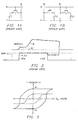
- FIG 2 there is illustrated a timing diagram for the operation of a ferroelectric memory cell.
- reading the value of a memory cell is destructive and the data value must be restored in the cell after the reading operation.
- the bit line gets charged by the switching charge of the cell while moving from a high logic value to a low logic value.
- the bit line charge differential may be used for the sensing operation as described herein above.
- the memory cell restoration takes place when the plate goes to a low logic value and the memory cell is driven to a high logic value and then finally back to its initial position when the bit line is driven to the low logic value.
- Imprint is a characteristic of ferroelectric films that refers to the tendency of a ferroelectric film/capacitor to prefer one polarization state over another polarization state. Imprint is known to occur when a ferroelectric capacitor is maintained in a single polarization state for a prolonged period of time. Imprint adversely effects the ability of a ferroelectric capacitor to switch between the polarization states. Consequently, the existence of imprint may directly impact the performance of a ferroelectric memory device.
- ferroelectric memory cells The performance of ferroelectric memory cells has been seen to degrade over time due to a number of other phenomena as well. For instance, ferroelectric memory cells may be effected by fatigue, endurance, retaining data over time, etc. When holding data over a prolonged period of time, such as under accelerated conditions during burn-in, a ferroelectric memory cell may be seen to degrade over the course of several hours or days.
- Figure 3 shows how a ferroelectric memory cell may be degraded, with the polarization characteristic being shown for a normal ferroelectric memory cell in a continuous set of lines and the polarization characteristic being shown for a degraded ferroelectric memory cell in dashed lines. At some point, a memory cell exhibiting degraded performance may store a charge in its ferroelectric capacitor that cannot be accurately sensed by a sense amplifier, thereby rendering the memory cell incapable of storing data values.
- Embodiments of the present invention are directed to a method and apparatus for testing the soundness of and determining the reliability risk in using a random access memory device, such as a ferroelectric random access memory device.
- the random access memory device includes an array of memory cells arranged in rows and columns associated with word lines and bit lines, respectively, sense amplifier circuitry selectively disabled during the testing of the random access memory device, address decode circuitry for selecting rows of memory cells within the array, and test circuitry for providing a current level corresponding to a voltage level appearing across the ferroelectric capacitor(s) of a memory cell connected to a selected bit line.
- Each bit line may be connected to and control the operating characteristics of a distinct transistor of the test circuitry, wherein each transistor is externally accessible when selected.
- the testing of the random access memory device may be performed by connecting memory cells in an addressed row to the bit lines of the array.
- the sense amplifiers are disabled when the random access memory device is under test.
- the bit lines are sequentially selected and a current is provided to a test pad having a level that is proportional to the voltage of the selected bit line. Because the voltage of the selected bit line is proportional to the voltage across the capacitor(s) of the memory cell connected thereto, the current level provided to the test pad is indicative of the voltage maintained by the memory cell.
- a mapping between the current level measured at the test pad and the voltage level of the selected bit line may be performed by a calibration circuit.
- the operating characteristics of the calibration circuit are substantially the same as the operating characteristics of the test circuitry.
- the mapping provides a relationship between a measured current and voltage applied to the calibration circuit which is substantially the same as the relationship between the current measured at the test pad and the voltage appearing at the selected bit line.
- the voltage at the bit line may be more accurately determined from the measured current at the test pad and the operating characteristics of the calibration circuit.
- Memory device 1 may be a nonvolatile memory device, such as a ferroelectric random access memory device. It is understood, however, that memory device 1 may be other memory devices as well. For instance, memory device 1 may include nonvolatile memory cells that may provide a degraded performance over time.
- the memory device 1 may be Dynamic Random Access Memory (DRAM), flash memory, Electrically Erasable Programable Read Only Memory (EEPROM), or Erasable Programable Read Only Memory (EPROM).
- DRAM Dynamic Random Access Memory
- EEPROM Electrically Erasable Programable Read Only Memory
- EPROM Erasable Programable Read Only Memory
- memory device 1 may itself form an integrated circuit chip or be a memory device that is embedded with other circuitry within an integrated circuit chip.
- Memory device 1 includes a memory cell array 2 of memory cells 3.
- Memory cells 3 may be ferroelectric memory cells that include one or more ferroelectric capacitor elements.
- Memory cell 3 may be implemented as a one transistor, one capacitor (1T1C) memory cell ( Figure 1A).
- memory cell 3 may be implemented as a two transistor, two capacitor (2T2C) memory cell ( Figure 1B).
- each memory cell 3 may be implemented in other ways using one or more ferroelectric capacitive elements or similar elements. It should also be understood that memory cell 3 may be a DRAM memory cell, a flash memory cell, or any other type of memory cell that may exhibit degraded performance.
- Memory cell array 2 may be arranged into rows and columns of memory cells 3.
- the memory cells 3 in a row of memory cells 3 may be connected to a distinct word line 7 and a distinct plate line 8.
- the memory cells 3 in a column of memory cells 3 may be connected to a distinct column/bit line 6 or a pair 5 of distinct column/bit lines.
- Figure 4 shows plate lines 8 being parallel to word lines 7.
- plate lines 8 can be coupled to more than one row of memory cells 3.
- plate lines 8 may be perpendicular to word lines 7.
- the voltage appearing across the ferroelectric capacitors in the memory cells 3 in rows that are not being accessed will not vary when the plate line 8 connected to such memory cells 3 is asserted. This is due to the fact that the transistor(s) in the unaccessed memory cells 3 are turned off, so the plate line 8 connected to the transistor simply follows the voltage change appearing on the capacitor plate connected to the asserted plate line 8.
- the plate lines 8 may be partitioned into smaller segments so that the plate lines 8 may be more easily driven.
- Memory device 1 may further include address logic 9, such as a row decoder circuit 9A, which receives an address value and asserts a word line 7 and plate line 8 pair corresponding to the address value; and column decoder circuit 9B, which receives the address value and connects one or more bit lines 6 to data input/output bus 12 via data input/output block 11.
- the row address decode circuit 9A drives the word line 7 to a voltage level so as to connect bit lines 6 to capacitive elements of memory cells 3 in the selected row. This causes the charge appearing in each memory cell 3 in the selected row to be shared with the charge (such as a zero charge) appearing on the corresponding bit line 6, thereby changing the voltage appearing on the corresponding bit line 6 accordingly.
- Sense amplifiers 10 are coupled to bit lines 6 and each may be controlled to sense a charge differential appearing across a pair of bit lines 6 and drive the bit lines 6 to the high voltage reference Vdd and low voltage reference Vss based upon the polarity of the charge differential.
- Data input/output (I/O) block 11 serves as an interface between bit lines 6 and the external (I/O) data bus 12, wherein addressed bit lines 6 are coupled thereto.
- a control circuit 13 provides necessary timing and control signals to memory cell array 2, address logic 9, sense amplifiers 10 and data input/output block 11 to preform read and write memory access operations when memory device 1 is in a normal mode of operation, and to control the testing of memory cells 3 when memory device 1 is in a test mode of operation. Control circuit 13 will be described in greater detail below.
- Memory device 1 is shown in Figure 4 as having a bidirectional external data I/O bus 12. It is understood that memory device 1 may include separate unidirectional data input and data output buses instead.
- memory device 1 includes test circuitry.
- the test circuitry may include a test circuit 20 that is adapted to sense the voltage level appearing across the capacitor elements of the ferroelectric memory cells 3 and provide externally to memory device 1 electrical signals representative of the sensed voltage level.
- Test circuit 20 is capable of operating during the testing and/or characterizing of memory device 1, such as during wafer sort. It is understood, however, that test circuit 20 may be used to analyze memory device 1 at times other than at wafer sort.
- Test circuit 20 produces a current which is representative of a voltage appearing on the bit line 6 after a selected ferroelectric memory cell 3 is connected thereto. Because the voltage on the bit line 6 is representative of the charge on the ferroelectric capacitor and the voltage thereon, the current level provided by test circuit 20 is proportional to the charge/voltage maintained by the memory cell 3 under test.
- the control circuit 13 may receive as an input a test input signal which, based on its value, configures the memory device 1 in the test mode of operation.
- sense amplifiers 10 are disabled by the control circuit 13 or otherwise disconnected from bit lines 6 so as to be incapable of sensing voltage levels appearing thereon. This results in memory device 1 being capable of performing memory read operations that are modified for testing memory cells 3.
- the control circuit 13 provides control for the operations of the memory device 1.
- Precharge/equilibrate circuitry may be controlled by the control circuit 13 so as to precharge the bit lines 6 to a predetermined voltage level, such as ground.
- FIG 5 illustrates an exemplary embodiment of the test circuit 20 for the memory device 1 of Figure 4.
- Each bit line 6 may be connected to a control terminal of one of a plurality of bit line (BL) connect transistors 22A-22N, with each BL connect transistor corresponding to a distinct bit line.
- a first terminal (source terminal) of each of the plurality of BL connect transistors 22A-22N may be connected to an external pad (Outpad) 15.
- the Outpad 15 is a pad capable of being connected to a tester probe (for wafer level testing) or a package pin (for post-packaging testing).
- the Outpad 15 is used to supply a voltage to the plurality of BL connect transistors 22A-22N and concurrently measure the level of current passing through a selected BL connect transistor 22A-22N, as will be explained in detail herein below.
- a second terminal (drain terminal) of each of the plurality of BL connect transistors 22A-22N may be connected to a first terminal (drain terminal) of one of a plurality of select transistors 24A-24N.
- the plurality of select transistors 24A-24N may be connected to ground through their second terminals (source terminals).
- the control terminals of the plurality of select transistors 24A-24N may be connected to control circuit 13 which in turn sequentially enables the plurality of select transistors 24A-24N.
- the control circuit 13 may include a decode circuit 26 and a counter 28.
- the counter may 28 receive as input a reset signal used to reset the counter 28 to a known state and a test clock (testclk) signal used to increment/decrement the counter 28.
- testclk test clock
- the counter 28 automatically increments/decrements through a number of states equal to the number of bit lines 6 in memory device 1.
- the decode circuit 26 may decode the output of the counter 28 and send a signal to one of the select transistors 24A-24N to enable that select transistor while disabling the other select transistors. Once a select transistor 24A-24N is enabled, the voltage appearing on the bit line associated with the enabled select transistor may be measured, as will be described hereinafter.
- the decode circuit 26 and the counter 28 may be included in the test circuit 20.
- the BL connect transistors 22 and the select transistors 24 as shown in Figure 5 are implemented by p-channel and n-channel MOS transistors, respectively. It should be understood that other types of field effect transistors, such as JFET and MESFET, may be used as well. It should also be understood that the BL connect transistors 22 may be implemented as n-channel transistors and the select transistors as p-channel transistors. However, a different configuration may be used to achieve the same functionality described above.
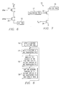
- Figure 6 illustrates an alternative implementation for the BL connect transistor 22 and the select transistor 24 of the test circuit 20 in Figure 5. In this case, the bit line 6 may be connected to the control terminal of the BL connect transistor 25 and the output of decode circuit 26 may be connected to the control terminal of the select transistor 23.
- the source terminal of the select transistor 23 may be connected to Vdd while the drain terminal may be connected to the drain terminal of the BL connect transistor 25.
- the source of the BL connect transistor 25 may be connected to the Outpad 15 where a voltage may be applied while a current is measured.
- a calibration may need to be performed.
- the calibration forms a matching/mapping relationship between the measured current levels at the Outpad 15 and the bit line voltage level appearing at the control terminal of the BL connect transistors 22A-22N. It should be understood that the calibration may be performed at any time relative to measuring current levels on Outpad 15.
- a calibration connect transistor 32 and a select transistor 34 may be p-channel and n-channel MOSFET transistors, respectively.
- the control terminal of the select transistor 34 may be connected to Vdd to turn it on.
- the source terminal of the select transistor 34 may be connected to ground and the drain terminal of the select transistor 34 may be connected to the drain terminal of the calibration connect transistor 32.
- the control terminal of the calibration connect transistor 32 may be connected to a calibration pad 17 and the source terminal may be connected to a test pad 16.
- the calibration test circuit 30 may be fabricated on the same memory chip as the test circuit 20 and thus the transistors of the calibration test circuit 30 have the same processing-related characteristics as the transistors of the test circuit 20.
- transistors 32 and 34 may have substantially the same dimensions as transistors 22A-22N and 24A-24N, respectively. In this way, the operating characteristics of calibration test circuit 30 will substantially match the operating characteristics of each pair of BL connect transistors 22 and select transistors 24.
- a voltage is applied at the test pad 16 (step 52) having a level such that a measurable amount of current can be measured at test pad 16.
- a voltage is applied at the calibration pad 17 (step 54) and the current is measured at the test pad 16 (step 56).
- the measured current at the test pad 16 corresponds to the applied voltage at the calibration pad 17.
- the voltage applied at the test pad 16 may be at a bias point such that the current can just be measured (i.e., transistor 32 is at the onset of conduction).
- the voltage applied to the calibration pad 17 is varied (i.e., decreased) and the current on the test pad 16 is measured for each of a plurality of voltage levels applied to calibration pad 17.
- a direct relationship between the applied voltage at the calibration pad 17 and the current measured at the test pad 16 may be recorded in a table (step 58).
- the relationship between the voltage level applied at the calibration pad 17 and the current measured at the test pad 16 is substantially the same as the relationship between the bit line voltage on the control terminal of the BL connect transistor 22 and the current measured at the Outpad 15.
- the table may be used to determine the voltage level appearing on the selected bit line 6 which itself is proportional to the voltage maintained by the selected memory cell 3.
- the calibration testing may be performed before or after the testing of the memory cell array 2.
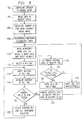
- memory device 1 may be configured into a normal mode of operation (step 102) by setting one or more input test signals to a first value.
- a plurality of write operations may be executed (step 104) so that each memory cell 3 stores a data value.
- Memory device 1 may be then configured in the test mode (step 106) by setting the one or more input test signals to a second value.
- the sense amplifiers 10 are disabled by the control circuit 13 when the memory device 1 is in the test mode.
- the bit lines 6 are equilibrated and precharged (step 108) to a predetermined voltage level. In an exemplary embodiment, the bit lines 6 are precharged to ground.
- Precharge/equilibrate circuitry (not shown) may be controlled by control circuit 13 to perform the precharge/equilibration of the bit line 6.
- a row of memory cells 3 is selected using the row decode circuit 9A by driving the selected word line to a Vdd voltage level (step 110) in response to application of an address input to the input of row decode circuit 9A.
- the counter 28 within the control circuit 13 is reset using a RESET test signal to put the value of the counter in a known state.
- a bit line 6 is then selected by manipulating testclk so that counter 28 and decode circuit 26 activate one of the select transistors 24 (step 112).
- a voltage is applied at the Outpad 15 (step 114) and the current is measured concurrently at the Outpad 15 (step 116).
- the applied voltage at the Outpad 15 is at a bias level to just allow the flow of the current (i.e., so that the selected BL connect transistor 22 is at the onset of conduction).
- This applied voltage is substantially the same as the voltage applied at the test pad 16 during the operation of calibration test circuit 30, as explained above with reference to Figures 7 and 8.
- the measured current at the Outpad 15 is proportional to the voltage appearing on the selected bit line 6, which is itself proportional to the voltage/charge maintained by the memory cell 3 connected to the selected bit line 6. Because the current-voltage relationship of calibration test circuit 30 is substantially the same as the current-voltage relationship of test circuit 20, the voltage level maintained by the memory cell 3 may be determined (step 124) using the table recorded in step 58 of Figure 8.
- the voltage level maintained by the memory cell 3 connected to the selected bit line 6 may be compared to a predetermined threshold voltage level (step 126) to determine if the memory cell 3 will be sufficiently usable over a prolonged period of time.
- the tested memory cell 3 may be deemed to be operating at an acceptable level.
- the selected memory cell 3 storing a logic zero data value and the voltage level being less than the threshold voltage level
- the tested memory cell 3 may be deemed to be operating at an acceptable level.
- the voltage level is below the predetermined threshold voltage level for logic one data values or above the predetermined threshold voltage level for logic zero data values, then the memory cell 3 may be marked as defective (step 130).
- step 114 may be performed at any time during the step of measuring the current (step 116).
- step 114 may be performed before the equilibration of the bit lines (step 108) and maintained throughout the time the current is measured.
- bit line 6 may be selected on the same row of memory cells by incrementing/decrementing the counter 28 by toggling test signal testclk.
- the output of counter 28 may be passed through the decode circuit 26 which in turn only activates another select transistor 24.
- Steps 114-118 are then repeated to test the memory cell 3 corresponding to the newly selected bit line 6.
- step 118 Once all the memory cells 3 in the selected row have been tested (step 118), another row of memory cells 3 is selected to test the memory cells 3 therein. This process is repeated until all the memory cells 3 in the array 2 have been tested.
- the memory cells 3 marked as unacceptable may be replaced by redundancy circuitry (not shown). Alternatively, the memory device 1 may be scrapped.
Landscapes
- For Increasing The Reliability Of Semiconductor Memories (AREA)
- Techniques For Improving Reliability Of Storages (AREA)
Abstract
Description
Claims (28)
- A random access memory device in an integrated circuit chip, comprising:a memory array of memory cells organized into rows and columns, including a plurality of word lines and bit lines, each row of memory cells being coupled to a word line and each column of memory cells being coupled to a bit line;sense amplifier circuitry coupled to the bit lines and being selectively disabled;address decode circuitry for receiving an address value and asserting a row line associated therewith; andtest circuitry, coupled to at least one bit line, for placing on an external pad of the integrated circuit chip a current level corresponding to a voltage level appearing on the at least one bit line, while concurrently disabling the sense amplifier circuitry.
- The random access memory device of claim 1, wherein the sense amplifier selectively drives the bit lines towards high and low reference voltage levels during normal memory access operations, the random access memory device is selectively configured in a test mode of operation by the test circuitry, and the sense amplifier circuitry is disabled from driving the bit lines by the test circuitry when the random access memory device is in the test mode of operation.
- The random access memory device of claim 2, wherein the random access memory device includes a test input signal and is selectively configured in the test mode of operation based upon a value of the test input signal.
- The random access memory device of any preceding claim wherein the external pad is sized to contact and electrically connect to a tester probe, and the test circuitry comprises a pair of series-connected transistors coupled between the external pad and a reference voltage level, the pair of series-connected transistors including a first transistor having a control terminal coupled to the at least one bit line.
- The random access memory device of any preceding claim wherein the external pad is sized to contact and electrically connect to a tester probe, and the test circuitry comprises a plurality of pairs of series-connected transistors coupled between the pad and a reference voltage level, each pair of series-connected transistors including a first transistor having a control terminal coupled to distinct bit line.
- The random access memory device of any preceding claim further comprising:calibration test circuitry for providing a relationship between the current level placed on the external pad and the voltage level appearing at the at least one bit line.
- A method of testing a semiconductor memory device having an array of memory cells and sense amplifier circuitry coupled to bit lines of the array, the semiconductor memory device being in an integrated circuit chip, the method comprising:connecting memory cells in a row of memory cells to bit lines of the array;disabling the sense amplifier circuitry from driving the bit lines;selecting a bit line; andproviding a current level to a pad in the integrated circuit chip corresponding to a voltage level appearing on the selected bit line.
- The method of claim 7, further comprising measuring the current level provided to the pad.
- The method of claim 7 or 8, further comprising:repeating the steps of selecting and providing, with each step of selecting comprising selecting a different bit line in the array.
- The method of claim 7,8 or 9, further comprising the step of:determining a relationship between the current level provided to the pad and the voltage level appearing on the selected bit line; andmapping the current level provided to a voltage level appearing across a memory cell connected to the selected bit line.
- The method of any of claims 7 to 10, further comprising the steps of:disconnecting the row of memory cells from the bit lines;connecting another row of memory cells to the bit lines; andrepeating the steps of selecting and providing for the another row of memory cells.
- An apparatus, comprising:a random access memory device, comprising:a memory array of memory cells organized into rows and columns, including a plurality of word lines and bit lines, each row of memory cells being coupled to a word line and each column of memory cells being coupled to a bit line;address decode circuitry for receiving an address value and asserting a row line associated therewith; andtest circuitry, coupled to at least one bit line for placing on an external pad a current level corresponding to a voltage level appearing on the at least one bit line.
- The device or apparatus or method of any preceding claim wherein the random access memory device comprises a ferroelectric memory device and/or a non volatile memory device.
- The apparatus of claim 12 or 13, wherein the random access memory device comprises sense amplifier circuitry that selectively drives the bit lines towards high and low reference voltage levels during normal memory access operations, the random access memory device is selectively configured in a test mode of operation by the test circuitry and the sense amplifier circuitry is disabled from driving the bit lines by the test circuitry when the random access memory device is in the test mode of operation.
- The apparatus of claim 12,13 or 14, wherein the apparatus further comprises:a processing unit having an address port connected to an address input port of the random access memory device and a data port connected to a data port of the random access memory device.
- The apparatus of any of claims 12 to 15, wherein the external pad is sized to receive a tester probe, and the test circuitry comprises a pair of series-connected transistors coupled between the external pad and a reference voltage level, the pair of series-connected transistors including a first transistor having a control terminal coupled to the at least one bit line.
- The apparatus of any of claims 12 to 16, wherein the external pad is sized to receive a tester probe, and the test circuitry comprises a plurality of pairs of series-connected transistors coupled between the external pad and a reference voltage level, each pair of series-connected transistors including a first transistor having a control terminal coupled to distinct bit line.
- The device or apparatus of any of claims 1 to 6 or 12 to 17, wherein the or each pair of series-connected transistors comprises a second transistor having a control terminal connected to a control signal that selectively activates the second transistor.
- The apparatus or device of claim 18, wherein the test circuitry comprises a selection circuit that selectively activates the second transistors of the plurality of pairs of series-connected transistors in a sequential manner.
- The random access memory device of claim 19, wherein the selection circuit comprises counter circuitry and decode circuitry having a plurality of output signals such that each output signal is connected to the control terminal of a distinct second transistor.
- The apparatus of claim 19, wherein the selection circuit comprises counter circuitry and decode circuitry having a distinct output signal connected to the control terminal of each of the second transistors.
- The device or apparatus of claim 1 or 12 or any claim appended thereto, wherein the test circuitry comprises:a first pair of series-connected transistors connected between the external pad of the apparatus or integrated circuit chip and a reference voltage level, a first transistor of the first pair of series-connected transistors having a control terminal connected to the at least one bit line; anda second pair of series-connected transistors connected between a second pad of the apparatus or integrated circuit chip and the reference voltage level, a first transistor of the second pair of series-connected transistors having a control terminal connected to a third pad of the apparatus and a second transistor of the second pair of series-connected transistors being activated.
- The apparatus of any of claims 12 to 22, wherein the random access memory device further comprises:calibration test circuitry for providing a relationship between the current level and the voltage level appearing at the at least one bit line.
- The apparatus or device of claim 23, wherein the calibration test circuitry has substantially the same structure as a portion of the test circuitry.
- The apparatus or device claim 22 or 24, wherein the calibration test circuitry comprises:an input connected to a second external pad for externally controlling the operating characteristics of the calibration circuit; andan output connected to a third external pad for externally measuring a current flowing through the calibration test circuitry.
- An apparatus, comprising:a ferroelectric capacitor; andmeans for placing on an external pad of the apparatus a current level corresponding to a voltage level appearing across the ferroelectric capacitor.
- The apparatus of claim 26, wherein the means for placing comprises a first transistor having a control terminal coupled to a plate of the ferroelectric capacitor, a first conduction terminal coupled to the external pad and a second conduction terminal coupled to a voltage reference.
- The apparatus of claim 27, wherein the means for placing further comprises a second transistor series connected to the first transistor to form a pair of series connected transistors connected between the external pad and the voltage reference, and a means for selectively activating the second transistor.
Applications Claiming Priority (2)
| Application Number | Priority Date | Filing Date | Title |
|---|---|---|---|
| US10/066,182 US6754094B2 (en) | 2002-01-31 | 2002-01-31 | Circuit and method for testing a ferroelectric memory device |
| US66182 | 2002-01-31 |
Publications (2)
| Publication Number | Publication Date |
|---|---|
| EP1333446A2 true EP1333446A2 (en) | 2003-08-06 |
| EP1333446A3 EP1333446A3 (en) | 2004-08-18 |
Family
ID=22067787
Family Applications (1)
| Application Number | Title | Priority Date | Filing Date |
|---|---|---|---|
| EP03250538A Withdrawn EP1333446A3 (en) | 2002-01-31 | 2003-01-29 | Circuit and method for testing a ferroelectric memory device |
Country Status (3)
| Country | Link |
|---|---|
| US (1) | US6754094B2 (en) |
| EP (1) | EP1333446A3 (en) |
| JP (1) | JP2003249074A (en) |
Families Citing this family (20)
| Publication number | Priority date | Publication date | Assignee | Title |
|---|---|---|---|---|
| US6714469B2 (en) * | 2002-07-02 | 2004-03-30 | Agilent Technologies, Inc. | On-chip compression of charge distribution data |
| US6804141B1 (en) * | 2003-05-20 | 2004-10-12 | Agilent Technologies, Inc. | Dynamic reference voltage calibration integrated FeRAMS |
| KR100505702B1 (en) * | 2003-08-20 | 2005-08-02 | 삼성전자주식회사 | Repair apparatus of semiconductor memory device capable of selectively programming in wafer test and in post package test and repair method of the same |
| GB2412468A (en) * | 2004-03-26 | 2005-09-28 | Zarlink Semiconductor Ab | Testing an EEPROM utilising an additional select transistor and test line |
| KR100627515B1 (en) * | 2004-10-04 | 2006-09-21 | 주식회사 하이닉스반도체 | Memory device and its test method |
| DE102005020808B3 (en) * | 2005-05-04 | 2006-07-20 | Micronas Gmbh | Memory cell programming and deletion controlling method for non-volatile memory device, involves producing positive or negative acknowledge information after process of programming or deletion of memory cell based on content of control cell |
| KR100702840B1 (en) * | 2005-07-13 | 2007-04-03 | 삼성전자주식회사 | Ferroelectric memory device and corresponding lighting section control method |
| JP5045364B2 (en) * | 2007-10-16 | 2012-10-10 | 富士通セミコンダクター株式会社 | Semiconductor memory device |
| JP2010218630A (en) * | 2009-03-17 | 2010-09-30 | Toshiba Corp | Semiconductor memory device and method of testing the same |
| US8724367B2 (en) * | 2010-12-30 | 2014-05-13 | Texas Instruments Incorporated | Method and apparatus pertaining to a ferroelectric random access memory |
| US8717800B2 (en) * | 2010-12-30 | 2014-05-06 | Texas Instruments Incorporated | Method and apparatus pertaining to a ferroelectric random access memory |
| US9003255B2 (en) | 2011-07-01 | 2015-04-07 | Stmicroelectronics International N.V. | Automatic test-pattern generation for memory-shadow-logic testing |
| KR101903520B1 (en) * | 2012-01-06 | 2018-10-04 | 에스케이하이닉스 주식회사 | Semiconductor apparatus |
| US9263100B2 (en) * | 2013-11-29 | 2016-02-16 | Freescale Semiconductor, Inc. | Bypass system and method that mimics clock to data memory read timing |
| KR102505721B1 (en) * | 2016-03-25 | 2023-03-06 | 에스케이하이닉스 주식회사 | Semiconductor Apparatus and Circuit for Measurement of Characteristic Therefor |
| DE102017121308B4 (en) | 2017-06-30 | 2019-06-06 | Taiwan Semiconductor Manufacturing Co., Ltd. | SYNCHRONOUS WRITE-THROUGH SAMPLING ARCHITECTURES FOR A MEMORY BLOCK |
| US10705934B2 (en) * | 2017-06-30 | 2020-07-07 | Taiwan Semiconductor Manufacturing Co., Ltd. | Scan synchronous-write-through testing architectures for a memory device |
| JP7175555B2 (en) * | 2018-03-09 | 2022-11-21 | エイブリック株式会社 | Test circuits and semiconductor devices |
| US10381071B1 (en) * | 2018-07-30 | 2019-08-13 | National Tsing Hua University | Multi-bit computing circuit for computing-in-memory applications and computing method thereof |
| US12488822B2 (en) * | 2023-01-20 | 2025-12-02 | Micron Technology, Inc. | Mitigating disturbance of digit lines at plate edges |
Family Cites Families (23)
| Publication number | Priority date | Publication date | Assignee | Title |
|---|---|---|---|---|
| JPS6122492A (en) | 1984-07-11 | 1986-01-31 | Hitachi Ltd | Dynamic ram |
| JP3348298B2 (en) | 1992-10-08 | 2002-11-20 | ソニー株式会社 | Cassette storage case |
| US5608679A (en) | 1994-06-02 | 1997-03-04 | Intel Corporation | Fast internal reference cell trimming for flash EEPROM memory |
| FR2728717B1 (en) * | 1994-12-21 | 1997-01-31 | Sgs Thomson Microelectronics | TEST METHOD AND CIRCUIT FOR AN INTEGRATED CIRCUIT MEMORY |
| JP3774500B2 (en) | 1995-05-12 | 2006-05-17 | 株式会社ルネサステクノロジ | Semiconductor memory device |
| US6052321A (en) * | 1997-04-16 | 2000-04-18 | Micron Technology, Inc. | Circuit and method for performing test on memory array cells using external sense amplifier reference current |
| US5966388A (en) * | 1997-01-06 | 1999-10-12 | Micron Technology, Inc. | High-speed test system for a memory device |
| US5764577A (en) * | 1997-04-07 | 1998-06-09 | Motorola, Inc. | Fusleless memory repair system and method of operation |
| JPH1117123A (en) * | 1997-06-23 | 1999-01-22 | Rohm Co Ltd | Non-volatile memory element |
| JPH1166890A (en) * | 1997-08-12 | 1999-03-09 | Mitsubishi Electric Corp | Semiconductor integrated circuit device |
| JPH11120797A (en) * | 1997-10-15 | 1999-04-30 | Toshiba Microelectronics Corp | Ferroelectric memory and screening method thereof |
| JP3727157B2 (en) * | 1997-11-19 | 2005-12-14 | Necエレクトロニクス株式会社 | Semiconductor memory device and test method thereof |
| JPH11154400A (en) | 1997-11-21 | 1999-06-08 | Toshiba Corp | Semiconductor memory device and test method therefor |
| JPH11261017A (en) * | 1998-03-16 | 1999-09-24 | Fujitsu Ltd | Semiconductor storage device |
| JP4587500B2 (en) | 1998-11-11 | 2010-11-24 | ルネサスエレクトロニクス株式会社 | Semiconductor integrated circuit, memory module, storage medium, and semiconductor integrated circuit relief method |
| US6452845B1 (en) * | 1999-01-07 | 2002-09-17 | Micron Technology, Inc. | Apparatus for testing redundant elements in a packaged semiconductor memory device |
| JP3718374B2 (en) * | 1999-06-22 | 2005-11-24 | 株式会社東芝 | Memory-embedded semiconductor integrated circuit device and test method thereof |
| JP2001291385A (en) * | 2000-04-05 | 2001-10-19 | Nec Corp | Semiconductor memory, its testing device, and testing method |
| JP3775716B2 (en) * | 2000-05-25 | 2006-05-17 | シャープ株式会社 | Ferroelectric memory device and test method thereof |
| US6359819B1 (en) * | 2000-12-29 | 2002-03-19 | Stmicroelectronics, Inc.. | Circuit and method for performing a stress test on a ferroelectric memory device |
| US6584007B2 (en) * | 2000-12-29 | 2003-06-24 | Stmicroelectronics, Inc. | Circuit and method for testing a ferroelectric memory device |
| DE10102432B4 (en) * | 2001-01-19 | 2005-09-22 | Infineon Technologies Ag | Test circuit for the analog measurement of bit line signals of ferroelectric memory cells |
| JP2002343099A (en) * | 2001-05-14 | 2002-11-29 | Toshiba Corp | Semiconductor storage device |
-
2002
- 2002-01-31 US US10/066,182 patent/US6754094B2/en not_active Expired - Lifetime
-
2003
- 2003-01-29 EP EP03250538A patent/EP1333446A3/en not_active Withdrawn
- 2003-01-31 JP JP2003023822A patent/JP2003249074A/en active Pending
Also Published As
| Publication number | Publication date |
|---|---|
| EP1333446A3 (en) | 2004-08-18 |
| US6754094B2 (en) | 2004-06-22 |
| US20030142565A1 (en) | 2003-07-31 |
| JP2003249074A (en) | 2003-09-05 |
Similar Documents
| Publication | Publication Date | Title |
|---|---|---|
| US6754094B2 (en) | Circuit and method for testing a ferroelectric memory device | |
| US8472236B2 (en) | Differential plate line screen test for ferroelectric latch circuits | |
| US6449184B2 (en) | Method for driving semiconductor memory | |
| US10573367B2 (en) | Setting of reference voltage for data sensing in ferroelectric memories | |
| US20030185041A1 (en) | Semiconductor memory device | |
| US10074422B1 (en) | 2T1C ferro-electric random access memory cell | |
| US6646905B2 (en) | Ferroelectric storage device | |
| US6816400B2 (en) | Circuit and method for testing a ferroelectric memory device | |
| US6658608B1 (en) | Apparatus and method for testing ferroelectric memories | |
| US6928376B2 (en) | Apparatus and methods for ferroelectric ram fatigue testing | |
| US6327682B1 (en) | Wafer burn-in design for DRAM and FeRAM devices | |
| US6826099B2 (en) | 2T2C signal margin test mode using a defined charge and discharge of BL and /BL | |
| US8248835B2 (en) | Semiconductor memory and test method for the semiconductor memory | |
| US6876590B2 (en) | 2T2C signal margin test mode using a defined charge exchange between BL and/BL | |
| US6359819B1 (en) | Circuit and method for performing a stress test on a ferroelectric memory device | |
| US7477536B2 (en) | Ferroelectric random access memory device and method of driving the same | |
| US6381185B2 (en) | Method and a circuit architecture for testing an integrated circuit comprising a programmable, non-volatile memory |
Legal Events
| Date | Code | Title | Description |
|---|---|---|---|
| PUAI | Public reference made under article 153(3) epc to a published international application that has entered the european phase |
Free format text: ORIGINAL CODE: 0009012 |
|
| AK | Designated contracting states |
Designated state(s): AT BE BG CH CY CZ DE DK EE ES FI FR GB GR HU IE IT LI LU MC NL PT SE SI SK TR |
|
| AX | Request for extension of the european patent |
Extension state: AL LT LV MK RO |
|
| PUAL | Search report despatched |
Free format text: ORIGINAL CODE: 0009013 |
|
| AK | Designated contracting states |
Kind code of ref document: A3 Designated state(s): AT BE BG CH CY CZ DE DK EE ES FI FR GB GR HU IE IT LI LU MC NL PT SE SI SK TR |
|
| AX | Request for extension of the european patent |
Extension state: AL LT LV MK RO |
|
| 17P | Request for examination filed |
Effective date: 20050207 |
|
| AKX | Designation fees paid |
Designated state(s): DE FR GB IT |
|
| RBV | Designated contracting states (corrected) |
Designated state(s): DE FR GB IT |
|
| STAA | Information on the status of an ep patent application or granted ep patent |
Free format text: STATUS: THE APPLICATION HAS BEEN WITHDRAWN |
|
| 18W | Application withdrawn |
Effective date: 20061010 |