BACKGROUND
This invention relates to a system and method for
processing an image and a compiler for use in this application,
and particularly relates to a system and method capable of
carrying out rapid data processing by reducing the number of
loading/storing operations when processing a large amount of
image data, and a compiler for use in this system.
In general, in the field of image processing technique,
such as computer graphics, it is desired to provide an image
processing system having a flexible image processing function
in order to realize various expressions relating to shape, color
and so forth in an image. Also with respect to a compiler serving
as software for use in this image processing system, it is desired
to provide a compiler capable of processing a large amount of
data relating to shape, color and so forth in a colorful image.
For example, in a case where color is determined on the
basis of a texture showing a pattern by brightness and color
in an image, the color of the image is determined on the basis
of coordinates of pixels forming the image. Also during this
processing for determining color, a large amount of data must
be used to be sequentially operated. For that reason, image
processing systems (Graphic Processor Units (GPUS)) for carrying
out rapid operation are conventionally used.
However, in conventional GPUs, it is possible to deal with
only fixed data flows or semi-fixed data flows, and the
processing of pixels capable of being executed at a time (by
one path. For that reason, it is required to use a plurality
of paths of GPUs in order to carry out a complicated operation.
In a case where a plurality of paths of GPUs are used, after
intermediate data is temporarily written in a memory, such as
a frame buffer, in the last path, data written in the memory,
such as the frame buffer, is read out of the memory in the
subsequent path, so that the number of loading/storing
operations increases with respect to the memory.
There is a problem in that the increase of the number of
loading/storing operations with respect to the memory causes
a bottle neck for the flow of data processing in the whole image
processor to reduce image processing performance, so that
improvements are desired from the standpoint of rapid data
processing. For example, the GeForce 3 GPU produced by "nVidia
Company" has a programmable pixel processor, and is capable of
programming an address operator and a combiner for blending pixel
color and so forth, by a series of instruction strings,
respectively (See Paper: GeForce 3 GPU [Compiling to a VLIW
Fragment Pipeline: Figures 1, 2]).
However, also in the chip produced by nVidia Company
disclosed in the above described paper, the number of
instructions capable of being executed with respect to one pixel
at a time is limited, and the number of registers is also limited.
Therefore, it is required to use a plurality of paths of pixel
processors to carry out a more complicated processing. The
reason for this is that the address operator is separated from
the combiner in the image processor serving as the prior art,
so that it is required to separate into a plurality of paths
when it is intended to carry out operation in order from the
combiner to the address operator.
If it is possible to provide an image processing system
for carrying out a more flexible processing by one path and a
compiler for use therein, it is possible to reduce the number
of paths in a pixel operation, and it is possible to reduce the
number of loading/storing operation in memory which tends to
be a bottle neck for performance.
SUMMARY OF THE INVENTION
An image processing system according to a first aspect
of the present invention comprises: a plurality of operation
pipelines to operate an inputted image data; a switching channel
to switch a data transfer path to input operation results, which
are outputted from the plurality of operation pipelines, to the
plurality of operation pipeline again; and a control circuit
to control switching of the data transfer path by the switching
channel and to control an operation in the plurality of operation
pipelines, the control circuit carrying out a scheduling of a
plurality of operations, which form (n-k+1) unit operations from
a unit operation k (1 < k < n) to a unit operation n (n is a
positive integer) of unit operations 1 to n, the plurality of
operations prevented from overlapping with each other at the
same predetermined operation time in the same operation pipeline
when a unit operation included in the plurality of operations
is executed by the plurality of operation pipelines.
A compiler according to a second aspect of the present
invention for use in an image processing system having a
plurality of operation pipelines to operate an inputted image
data; a switching channel to switch a data transfer path to input
operation results, which are outputted from the plurality of
operation pipelines, to the plurality of operation pipeline
again; and a control circuit to control the switching of the
data transfer path by the switching channel and to control an
operation in the plurality of operation pipelines, the compiler
comprising receiving a part of the image data supplied from the
outside each operation pipeline included in the plurality of
operation pipelines, and scheduling a plurality of operations,
which form (n-k+1) unit operations from a unit operation k (1
< k < n) to a unit operation n (n is a positive integer) of n
unit operations from 1 to n forming the plurality of operations,
the plurality of operations prevented from overlapping with each
other at the same operation time in the same operation pipeline,
and controlling a sequence of operations in the plurality of
operation pipelines in accordance with scheduling.
An image processing method according to a third aspect
of the present invention comprises: supplying a part of inputted
image data, which is supplied from the outside, to each operation
pipeline forming a plurality of operation pipelines to operate
the image data; carrying out a scheduling of a plurality of
operations, which form (n-k+1) unit operations from a unit
operation k (1 < k < n) to a unit operation n (n is a positive
integer) of n unit operations from 1 to n forming the plurality
of operations, the plurality of operations prevented from
overlapping with each other at the same operation time in the
same operation pipeline; and controlling the operation of the
image data in accordance with the scheduling.
BRIEF DESCRIPTION OF THE DRAWINGS
FIG. 1 is a block diagram showing the whole configuration
of an image processing system according to a first embodiment
of the present invention is provided; FIG. 2 is a block diagram showing a schematic construction
of an image processing core in FIG. 1; FIG. 3 is a block diagram showing a schematic functional
construction in an image core; FIG. 4 is an illustration for explaining the operation
of the image processing core in FIGS. 1 through 3, wherein (a)
shows a data flow graph (DFG = unit operation), (b) shows a unit
operation scheduled by two functional units (FUs), and (c) shows
the schedule of two FUs; FIG. 5 is an illustration showing the relationship
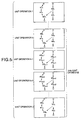
between unit operations 1 to n and each operation; FIG. 6 is an illustration showing (a) Example 1 shifted
by one cycle and (b) Example 2 shifted by three cycles, in which
scheduling can not be carried out due to the overlapping of
operations; FIG. 7 is an illustration for explaining the operation
of the image processing core in FIGS. 1 through 3, wherein (a)
shows a data flow graph (DFG = unit operation), (b) shows a unit
operation scheduled by three functional units (FUs), and (c)
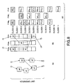
shows the schedule of three FUs; FIG. 8 is an illustration for explaining the operation
of the image processing core in FIGS. 1 through 3, wherein (a)
shows a data flow graph (DFG = unit operation), (b) shows a unit
operation scheduled by three functional units (FUs), and (c)
shows the schedule of three FUs, which are different from those
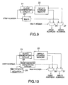
in FIG. 5; FIG. 9 is a block diagram showing the construction of an
address generating circuit when a base address is equal to a
"step number mod N"; FIG. 10 is a block diagram showing the construction of
an address generating circuit when a base address is equal to
a "generation * base address step width mod N"; FIG. 11 is an illustration showing an example of the
reduction of the number of branches in the case of a four-pixel
blending processing serving as an example of an operation; FIG. 12 is an illustration showing a channel an operation
pipeline when a channel in an FU is realized by a FIFO or the
like; FIG. 13 is a block diagram showing an example of a pipeline
for carrying out a multiplication and subtraction for concretely
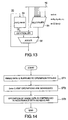
enabling the processing of FIG. 12; and FIG. 14 is a flow chart showing processing steps of the
third embodiment of an image processing method according to the
present invention.
DESCRIPTION OF THE EMBODIMENTS
Referring now to the accompanying drawings, the
embodiments of a system and method for processing an image and
a compiler for use in this system according to the present
invention will be described below. First, referring to FIG. 1,
the whole system configuration of the first embodiment of an
image processor will be described. It is an object of the
construction in this first embodiment to provide an image
processor for efficiently carrying out various image processes.
First, an example of a configuration of a system using a processor
in the first embodiment will be described.
FIG. 1 shows an example of a configuration of an image
processing system to which the first embodiment of an image
processor according to the present invention is applied. In this
figure, an image processor 1 comprises an image processing
dedicated circuit 2, such as a Setup/DDA, a memory 3 mounted
on the same chip, and at least one, preferably a plurality of
image processing cores 4. The detailed construction of the image
processing core 4 will be described later.
The image processor 1 is connected to a central processing
unit (which will be hereinafter referred to as a CPU) via a system
bus 5, and is associated with the CPU 6 to carry out information
processing including an image processing. The image processor
1 is also connected to an external memory unit 8 via the system
bus 5 and a bridge 7, and carries out an information processing
while transmitting and receiving data to and from the memory
unit 8. To the bridge 7, an input/output part 9 is also connected.
Each of the image processing cores 4 includes a controller 10
which controls components in each core.
Referring to FIG. 2, the details of the image processing
core 4 will be described below. FIG. 2 schematically shows the
image processing core 4. The image processing core 4 comprises,
in addition to the above described controller 10, a first loading
unit 12, a plurality of operation pipelines 17 and 18 which are
pipeline-like operators to carry out a pixel operation, a
switching channel 15, and an internal bus 16 which functions
as a communication path. The controller 10 carries out a
scheduling so as to prevent a plurality of operations, which
constitute (n-k+1) unit operations from a unit operation k (1
< k < n) to a unit operation n (n is a positive integer) of n
unit operations from 1 to n, from overlapping with each other
at the same operation time in the same operation pipeline when
the plurality of operation pipelines 17 and 18 execute an unit
operation including a plurality of operations in the pipelines
(the details will be described later).
The image processing core 4 receives at least a part of
image data from the memory 3 via the first loading unit 12 to
process the data by each of the operation pipelines 17 and 18
of an operation pipeline group to rewrite a series of data in
the memory 3 via the store unit 11 to carry out an information
processing. At this time, the switching channel 15 and the
internal bus 16 are used for executing a program having a DAG
(Directed Acyclic Graph) -like data flow. A method for executing
this program will be described later.
By enabling the execution of the program having the
DAG-like data flow, the number of loading/storing operations
in the memory can be reduced in comparison with conventional
GPUs capable of executing only a fixed data flow. In order to
realize this, although the amount of hardware slightly increases
by the addition of the switching channel 15 and the internal
bus 16, the number of loading/storing operations tending to be
a bottle neck on performance can be reduced, so that the
improvement of the whole performance can be expected.
Referring to FIG. 3, an example of a functional
construction of an image processing core 4 will be described
below.
FIG. 3 is a block diagram showing an example of a
construction of an image processing core 4. In the case of the
image processor in this first embodiment, the image processing
core 4 comprises a controller 10, a storing unit 11, a first
loading unit 12, a switching channel 15, an internal bus 16,
a first operation pipeline (FUa) 17, and a second operation
pipeline (FUb) 18.
The controller 10 controls other components every step
by particularly using a concept called phase. The phase is
herein defined by Phase = Step Number mod Maximum Phase Number.
Since the phase can be grasped as an operation clock in a concrete
operation stage in the operation pipelines 17 and 18, the phase
will be expressed as a clock in the subsequent explanation.
The FUa 17 and FUb 18 are pipelined operation pipeline,
and can execute different instructions every a predetermined
operation time, i.e., every phase (clock in FIG. 4). The
switching channel can comprise a group of channels and cross
bars. These cross bars are single direction cross bars capable
of carrying out a multicast (an input set does not overlap with
an output set). The cross bar can feed the output of the
operation pipeline to an optional channel every clock, and can
feed the output of an optional channel to the input of an optional
operation pipeline every clock. The switching channel 15 is
formed by putting a plurality of channels (IR/IW RAM) together.
Each channel of the switching channel 15 can read on the basis
of a read offset address determined every clock, and write on
the basis of a write offset address.
With such a construction, it has a higher programmability
than that of a register combiner type GPU, such as the GeForce
3, and can control a larger number of operators with a more area
efficiency than those of a VLIW type processor.
The compiler for use in the second embodiment of an image
processing system according to the present invention is an image
processing program executed in the image processor 1. This
compiler carries out a scheduling so that each of operation
pipelines forming a plurality of operation pipelines receives
part of the image data, which is supplied from the outside, to
prevent a plurality of operations, which are (n-k+1) unit
operations from a unit operation k (1 < k < n) to a unit operation
n (n is a positive integer) of n unit operations from 1 to n,
from overlapping with each other at the same operation time in
the same operation pipeline, and control the sequence of
operation in the plurality of operation pipeline in accordance
with the scheduling.
Referring to FIG. 4, an example of execution of a program
in the image processor in the first embodiment will be described
below. FIG. 4 shows an example of a program capable of being
executed by the image processing core 4, and its schedule. FIG.
4(a) shows a DFG (Data Flow Graph) to be executed. This DFG
constitutes a unit operation serving as a repeated pattern for
a series of operations. That is, in the figure, reference sign
a0, a1, a2, b0 and b2 correspond to the respective operations
in the operation pipeline (FU), and a set of a series of
operations a0, a1, a2, b0 and b2 is a unit operation, arrows
connecting the respective operations in the unit operation
corresponding to transfer between operation pipelines, upper
white circles in the figure meaning inputs, and lower white
circles in the figure meaning outputs.
FIG. 4(b) shows a unit operation after scheduling. It
is assumed that a0, a1 and a2 can be executed by the first
operation pipeline (FUa) 17 and b0 and b2 can be executed by
the second operation pipeline (FUb) 18. The FUa 17 and FUb 18
can execute different instructions every clock. In this example,
the FUa 17 executes the operation a0 at clock 0, and the operation
a2 at clock 4. The FUb executes b0 at clock 1, and the operation
b2 at clock 5. The maximum clock is 3, and one operation pipeline
FU is set so as to be capable of executing one operation during
three clocks.
FIG. 4(b) notes one unit operation based on a set of input
data. A series of processes in one unit operation is called
generation. A set of input data which is different every step
is inputted during execution, and a plurality of generations
of processes are simultaneously executed. FIG. 4(c) shows the
state of the processing. In this figure, a plurality of
operations with slant lines are unit operations of the same
generation k.
In FIG. 4(c), the operations of the k-th generation of
the unit operation are carried out at the same clock. The FUa
17 executes an operation a0k at clock 0, a1k at clock 2, and an
operation a2k at clock 4. The FUb executes b0k at clock 1, and
an operation b2k at clock 5. With respect to the unit operation
of the next generation k+1, the FUa 17 executes an operation
a0k+1 at clock 3, a1k+1 at clock 5, and an operation a2k+1 at clock
7, and the FUb executes b0k+1 at clock 4 and an operation b2k+1
at clock 8.
Referring to FIG. 5, the relationship between unit
operations and respective operations. The image processor
sequentially processes n unit operations from a unit operation
1 to a unit operation n, and the sequence of the respective
operations in each unit operation is the same sequence.
Therefore, the processes in a plurality of operation pipelines
must schedule so as to prevent the respective operations in the
same unit operation overlap with each other at the same clock
and so as to prevent operations in the adjacent unit operations
and unit operations at some intervals from overlapping from each
other at the same clock in the same pipeline.
That is, when the respective operation pipelines 17 and
18 constituting a group of operation pipelines receive part of
a series of data which are fed from the outside to be held in
the memory and when the controller 10 schedule so as to use the
plurality of pipelines 17 and 18 to operate a unit operation
comprising a plurality of operations during the plurality of
operation times, if the unit operations are unit operations 1
to n (n is a positive integer), the controller 10 controls the
sequence of operations so as to prevent each operation in the
k-th (1 < k < n) unit operation from overlapping with each other
and each operation in the k+1-th and k+2-th unit operations from
overlapping with each other at the same operation time in the
same pipeline and so as to prevent each operation in the (n-k+1)
unit operations from k to n from overlapping with each other
at the same operation time (clock) in the same pipeline 17 or
18.
FIG. 6(a) shows an example 1 where scheduling overlaps
if being shifted by one cycle, and FIG. 6(b) shows an example
2 where scheduling overlaps if being shifted by three cycles.
In the example 1 shown in FIG. 6(a), there is shown a case where
unit operations are executed so that a0k is executed at clock
0, a1k is executed at clock 1, a2k is executed at clock 2, ···,
although the sequence of operations in the unit operation is
the same as that in FIG. 4(a). As shown in FIG. 4(b), if
scheduling is not carried out so that the FUa operates at clocks
0, 2 and 4 and does not operate at clocks 1 and 3 therebetween
and if the respective pipelines are used at continuous clocks
for carrying out a parallel operation, the respective operations
in the unit operation k are carried out so that the FUa carries
out the operation a0k at clock 0, the operation a1k at clock 1
and the operation a2k at clock 2 and the FUb carries out the
operation b0k at clock 1 and the operation b2k at clock 3. Then,
if scheduling is carried out a clock shifted by one cycle to
carry out the unit operation k+1 in the next generation,
scheduling is carried out so that the FUa operates a0k+1 at clock
1, a1k+1 at clock 2 and a2k+1 at clock 3 and the FUb operates b0k+1
at clock 2 and b2k+1 at clock. In this case, as shown in blocks
with slant lines in FIG. 6(a), two operations in different
generations are scheduled at clocks 1 and 2 in the FUa, so that
the operations overlap with each other at a specific clock in
the FUa.
FIG. 6(b) shows a case where the next unit operation is
shifted by three cycles after the same unit operation as that
in FIG. 4(a) is scheduled in the same manner as that in FIG.
4(c). In this case, although the unit operation k is carried
out by the same scheduling as that in FIG. 4(c), the unit
operation k+1 in the next generation is carried out so as to
operate a0k+1 at clock 3, a1K+1 at clock 5 and a2k+1 at clock 7 in
the FUa and so as to operate b0k+1 at clock 4 and b2k+1 at clock
7 in the FUb. Therefore, as shown in blocks with slant lines
in FIG. 6(b), the operations b2k and b0k+1 overlap with each other
at clock 4 in the FUb. Also at clock 7 in the FUb, the operations
b2k+1 and b0k+1 overlap with each other. In order to avoid such
overlapping of operations, it may be studied whether the
respective operations collide with each other with respect to
the unit operation as described in FIG. 5, and scheduling shown
in FIG. 4(c) may be carried out.
By thus operating the operation pipeline after previously
scheduling, it is possible to efficiently execute the operations
of the plurality of operation pipelines every clock without
wasting, so that it is possible to simply carry out efficient
control of operators and communication paths. Furthermore,
since instructions to be executed by clocks in each operation
pipeline have been determined, corresponding instructions may
be sequentially executed every clock.
Furthermore, the programs executed by the image processor
and their scheduling methods shown in FIGS. 4(a), 4(b) and 4(c)
are examples. By providing three FUs in the operation pipeline,
clocks being predetermined operation times may be two cycles
to repeat operations. Such examples are shown in FIGS. 7 and
8. A unit operation shown in FIG. 7(a) is scheduled as shown
in FIG. 7(b) to operate as shown in FIG. 7(c). There are three
operation pipelines FUa0, FUa1 and FUb. The FUa0 and FUa1 carry
out the same operation as that in FIG. 4 by substituting two
pipelines for the function of the pipeline FUa in FIG. 4 and
by repeating two clocks. Thus, the operations a0, a1 and a2 may
be distributed in two operators FUa0 and FUa1.
If two operation pipelines are used for scheduling a unit
operation as shown in FIGS. 4(b) and 4(c), six blocks from clock
0 to clock 5 are used for carrying out, e.g., the unit operation
k. However, if three operation pipelines are used for scheduling
a unit operation as shown in FIGS. 7(b) and 7(c), the same unit
operation k can end by three clocks from clock 2 to clock 4,
so that one unit operation can be completed by half cycles by
adding only one operation pipeline.
FIGS. 8(a), 8(b) and 8(c) show a case where operations
a0, a1 and a2 are distributed in two operators FUa0 and FUa1
similar to FIG. 7 and where operations a0 and a1 and operations
b0 and b1 in the respective operation pipelines FUa0 and FUb
are spaced from each other by two clocks or more. Even if the
number of the operation pipelines is increased by one to
substitute two clocks for one clock in one of the operation
pipelines, one unit operation may be completed by four clocks
as shown in FIGS. 7(a), 7(b) and 7(c) or may be carried out by
six clocks as shown in FIGS. 8(a), 8(b) and 8(c).
Furthermore, if operation is carried out as shown in FIG.
8, the operation b0 in the unit operation k+1 is executed prior
to the operation b1 in the unit operation k. Thus, the operation
in the unit operation to be subsequently executed can be executed
prior to the operation in the unit operation to be executed before
the operation to be subsequently executed. The feature of the
example in FIG. 8 compared with that in FIG. 7 is that such
scheduling can be carried out so that the sequence of operations
is replaced.
The control of the switching channel 15 is carried out
every channel (1R/1W·RAM). Specifically, a read address and
a write address are determined every channel. FIG. 9 shows the
operation for determining the addresses in the channel. For
example, the read and write addresses are determined as follows.
Assuming that N is the number of entries denoting the
number of addresses in the memory,
Base Address = (Generation Counted Value * Channel Multiplicity
(Channel)) mod N
Read Address = (Base Address + Read Offset (Ch, phase) mod N
Write Address = (Base Address + Write Offset (Ch, phase) mod
N
where the generator counter is a value counted up every clock
0. Since the base address is a value of modulo N, the base address
can be realized every clock 0 by the counter (cycle counter)
of the modulo N counted up every channel multiplicity. This will
be hereinafter referred to as a base address counter.
The channel multiplicity is a value (natural number)
indicative of the number of branches to be embedded in one channel,
the branches indicating different data on a unit operation, and
is determined every channel. The read and write offsets are
determined every channel and every clock. Therefore, the
control circuit every channel can be realized by a base counter
and a circuit for reading read and write offsets every clock
from a table to carry out a modulo addition to a value of a base
address.
The block diagrams of FIGS. 9 and 10 show concrete examples
of the controllers of FIGS. 1 through 3. FIG. 9 shows a
functional construction of an address counter when a base address
is equal to a step number mod N. In FIG. 9, a step number is
inputted to a clock generating circuit 21 and a modulo N circuit
23, and a read address and a write address are outputted from
adders 26 and 27 on the basis of an offset, which is read out
of an offset storage memory 22, and an output of the modulo N
circuit 23 on the basis of the output of the clock generating
circuit 21.
FIG. 10 shows an example for obtaining a base address on
the basis of a quotient which is obtained by dividing a step
by the number of clocks when generation is determined. For
example, when a graph is executed every two steps, one is counted
up every two cycles. An offset is obtained in the same manner
as that in the example of FIG. 8, and a base address is outputted
from a base address generator 25 on the basis of the output of
a multiplicity register 24 and the number of inputted steps.
The base address is obtained by "Base Address = Generation *
Base Address Step Width mod N", and the base address thus obtained
is outputted to adders 26 and 27 in the same manner as that in
FIG. 9.
The adders 26 and 27 add the offsets and base addresses,
which are outputted from the offset storage memory 22, to output
read addresses and write addresses, respectively. According to
the address generating circuit in the example of FIG. 9, the
base address step width can be a smaller value than the number
of clocks, so that it is possible to more effectively use the
memory than the base address generating circuit shown in FIG.
9.
FIG. 11 shows an example of the reduction of the number
of branches by increasing the function of an operator. FIG. 11
shows a case where a processing for blending four pixels in image
data is carried out, wherein "a" means an operation for reading
a pixel, and "b" means an operation for carrying out a pixel
operation, "c" meaning an operation for reading four pixels to
carry out a pixel operation. According to this example of
operation, the number of branches on the left side of an outline
arrow is eleven, whereas the number of branches on the right
side thereof is two.
By thus increasing the function of the operator, it is
possible to reduce the number of branches, and it is possible
to decrease the scale of cross bar and channel. With such a
construction, it can be applied to a circuit for reading a
plurality of pixels with a filtering function which will be
described later.
The image processing system according to the present
invention may have the arrangement of a plurality of image
processing cores. This is a construction wherein a plurality
of image processing cores are arranged on one semiconductor chip,
and can linearly improve performance by integrating a plurality
of image processing cores. Since this has a scalability capable
of executing a unit operation having a free scale to some extent
by an image processing core alone, it is possible to execute
a unit operation having a free scale to some extent even if the
connection between the image processing cores is rough. Since
the image processing core itself is a pipelined operator, an
operator can be carried out in one throughput every cycle or
every some cycles, so that the image processing core can be used
as an operation pipeline for conventional image processors.
As described above, the image processing system according
to the present invention use an concept that the flow of each
operation processing in a unit operation is scheduled before
execution of the operation. Although FIG. 4(a) shows the
contents of the operation, the contents of the operation do not
show the number of operation pipelines constituting the system.
Therefore, the present invention does not depend on whether the
number of operation pipelines capable of executing the
operations a0, a1 and a2 is one or two. Each operation shown
in FIG. 4(a) can be called a virtual operation pipeline.
By previously assigning a unit operation before
scheduling as a program and by carrying out a detailed scheduling
after the concrete configuration of the system is understood
during execution, the program can be an independent construction
from the system configuration. This is conceptually grasped to
be the above described compiler serving as the second
construction. Thus, even if the configuration of the system is
changed, the same program can be executed. Specifically, it is
possible to change the number of operation pipelines, the
throughput of the operation pipelines, and latency, and so forth.
Although the connections between operation pipelines are
limited in conventional image processors having a chaining
function, the image processing system serving as the first basic
construction according to the present invention can execute an
optional DAG-like data flow program if the number of operation
pipelines and the number of channels are allowed. Therefore,
it is possible to reduce the number of loading/storing operations.
In addition, since the operation pipeline can execute different
instructions every clock, the number of vertexes constituting
an executable DAG is not limited to the number of operation
pipelines, so that it is possible to reduce the number of
loading/storing operations in comparison with conventional
image processors which do not have any virtual functions for
operation pipelines.
Moreover, since the scheduling for operation pipelines
is previously carried out every unit operation, it is possible
to simplify the control circuit. A SIMD type processor can
realize the same function by a software pipelining. However,
if the function is realized by the SIMD type processor, a register
file requires read ports, the number of which is equal to the
total number of inputs of an operation unit, write ports, the
number of which is equal to the total number of outputs of the
operation unit, and registers, the number of which is (the number
of channels x the mean depth of channels) or more. Therefore,
it is required to provide a large scale of system, so that the
proposed system is advantageous.
If the output path of the channel comprises a single-directional
cross bar which is capable of carrying out a
multicast and wherein a set of inputs do not overlap with a set
of outputs, when a data flow program is executed, a plurality
of channels for transferring the same data to the same step can
be integrated to be replaced with one channel and a multicast
in a channel output communication path. For that reason, it is
possible to reduce the number of channels required to execute
the same data flow program, and it is possible to decrease the
scale of the system. The scale of the data flow graph (DFG =
unit operation) capable of being realized by the same number
of channels increases, so that it is possible to reduce the number
of loading/storing operations.
If a channel constituting a group of channels comprise
a random access memory and if the random access memory is formed
so as to be capable of writing one data at an optional address
every one step and reading one data from an optional address,
when a data flow program is executed, a plurality of channels
for transferring the same data to different steps, so that one
channel can be substituted for the channel constituting the group
of channels. Thus, the scale of the system can be reduced, and
the number of loading/storing operations can be reduced.
If the control circuit is formed so as to have the function
of controlling to carry out the transfer between the same
pipelines by a communication path provided in an operation
pipeline, the number of used channels can be reduced, there are
characteristic effects in that the scale of the system is reduced
and the number of loading/storing operations is reduced. FIG.
12 shows an example of a channel capable of being reduced.
By forming such a construction by a FIFO (First-In
First-Out) circuit, the above described function can be realized
by a simple system. In comparison with the above described
construction, although conditions for reducing the number of
used channels are slightly severe, the number of used channels
can be efficiently reduced by scheduling instructions so as to
be capable of reducing the channels during compile. FIG. 13
shows an example of an operation pipeline.
In FIG. 13, a FIFO circuit 30 comprises a multiplier 31
for multiplying image data supplied via, e.g., the internal bus
16 in FIGS. 2 and 3, an adder 32, one input of which is the output
of the multiplier 31, a first-in first-out (FIFO) part 33 for
receiving the output of the adder 32 to output in the input
sequence by the first-in first out operation, and a controller
10 for synthesizing and outputting, e.g., address information
inputted to the output of the FIFO part 33 via the internal bus
16. To the other input of the adder 32, the output of the
controller 10 is fed.
This example is a pipeline for carrying out the MUL-ADD
(a+b*c), and a channel is provided for returning the operation
results to the input a. If the plurality of operation pipelines
include an operation pipeline for carrying out an operation
relating to color of an image, a complicated DAG often required
for a graphic processor can be executed by a small number of
loading/storing operations by using the proposed system for the
graphic processor.
Finally, referring to the flow chart of FIG. 14, the third
embodiment of an image processing method according to the present
invention will be described below. In FIG. 14, at step ST1, at
least part of image data supplied from the outside is fed to
each operation pipeline constituting a plurality of pipelines
for operating the inputted image data.
Then, at step ST2, (n-k+1) unit operations from a unit
operation k to a unit operation n (n is a positive integer) of
n unit operations from 1 to n, the unit operation comprising
a plurality of operations, are scheduled so as not to overlap
with each other at the same operation time in the same pipeline.
A concrete example of this unit operation is shown in FIG. 4(a).
Then, as shown at step ST3 in FIG. 14, the operation of
the image data is controlled in accordance with the scheduling
carried out at step ST2. By the above described steps, the image
data is processed.
As described above in detail, the present invention can
provide an image processing system and method capable of reducing
the number of paths in an image processing operation, the objects
of which are various processes, to efficiently carry out the
processes, and reducing the number of loading/storing operations
in a memory, by processing data by an operating part for carrying
out a parallel processing after previously scheduling data,
which is read by one memory access and which is to be processed,
when a large amount of data relating to the shape and color of
an image is processed, and a compiler for use in this system.
In addition, since the scheduling of operation pipelines is
previously carried out every unit operation, the construction
of the control circuit of the image processing system can be
simplified.