EP1333317A2 - Nonlinear optical switch - Google Patents
Nonlinear optical switch Download PDFInfo
- Publication number
- EP1333317A2 EP1333317A2 EP02015383A EP02015383A EP1333317A2 EP 1333317 A2 EP1333317 A2 EP 1333317A2 EP 02015383 A EP02015383 A EP 02015383A EP 02015383 A EP02015383 A EP 02015383A EP 1333317 A2 EP1333317 A2 EP 1333317A2
- Authority
- EP
- European Patent Office
- Prior art keywords
- optical
- light
- optical switch
- optical signal
- nonlinear
- Prior art date
- Legal status (The legal status is an assumption and is not a legal conclusion. Google has not performed a legal analysis and makes no representation as to the accuracy of the status listed.)
- Withdrawn
Links
Images





Classifications
-
- G—PHYSICS
- G02—OPTICS
- G02B—OPTICAL ELEMENTS, SYSTEMS OR APPARATUS
- G02B26/00—Optical devices or arrangements for the control of light using movable or deformable optical elements
- G02B26/08—Optical devices or arrangements for the control of light using movable or deformable optical elements for controlling the direction of light
-
- G—PHYSICS
- G02—OPTICS
- G02F—OPTICAL DEVICES OR ARRANGEMENTS FOR THE CONTROL OF LIGHT BY MODIFICATION OF THE OPTICAL PROPERTIES OF THE MEDIA OF THE ELEMENTS INVOLVED THEREIN; NON-LINEAR OPTICS; FREQUENCY-CHANGING OF LIGHT; OPTICAL LOGIC ELEMENTS; OPTICAL ANALOGUE/DIGITAL CONVERTERS
- G02F1/00—Devices or arrangements for the control of the intensity, colour, phase, polarisation or direction of light arriving from an independent light source, e.g. switching, gating or modulating; Non-linear optics
- G02F1/35—Non-linear optics
- G02F1/3515—All-optical modulation, gating, switching, e.g. control of a light beam by another light beam
-
- G—PHYSICS
- G02—OPTICS
- G02F—OPTICAL DEVICES OR ARRANGEMENTS FOR THE CONTROL OF LIGHT BY MODIFICATION OF THE OPTICAL PROPERTIES OF THE MEDIA OF THE ELEMENTS INVOLVED THEREIN; NON-LINEAR OPTICS; FREQUENCY-CHANGING OF LIGHT; OPTICAL LOGIC ELEMENTS; OPTICAL ANALOGUE/DIGITAL CONVERTERS
- G02F2201/00—Constructional arrangements not provided for in groups G02F1/00 - G02F7/00
- G02F2201/06—Constructional arrangements not provided for in groups G02F1/00 - G02F7/00 integrated waveguide
- G02F2201/066—Constructional arrangements not provided for in groups G02F1/00 - G02F7/00 integrated waveguide channel; buried
Definitions
- the present invention relates to an optical switch and, more particularly, to an optical switch capable of operating at low power consumption, excellent in response speed, and having construction suitable for miniaturization and multichannelling.
- WDM system wavelength division multiplexing system
- a switching means for switching optical information is essential to achieving further rapid optical communication.
- a conventional optical information switching method needs light-to-electricity conversion means for converting optical information into corresponding electrical information and electricity-to-light conversion means for converting electrical information into corresponding electrical information at relay points. Total power consumption by the light-to-electricity conversion means and electricity-to-light conversion means increases and switching speed decreases with the increase of the number of relay points. Therefore, it is preferable that a rapid optical communication system employs optical switches capable of directly switching optical information.
- Known optical switches including a mechanical optical switch, a plane optical waveguide optical switch, a mirror optical switch, and a bubble optical switch are mentioned in, for example, Nikkei Electronics, No. 8 (Jan. 29, 2000).
- Those conventional optical switches need a switching time on the order of milliseconds and have difficulty in coping with future increases in capacity and communication speed of optical communication systems.
- the conventional optical switches require high electrical driving force for operation and consume much energy.
- Japanese Patent Laid-open No. 11-337988 proposes an all-optical switch provided with nonlinear optical members and capable of quick response.
- This prior art optical switch has two nonlinear optical members and controls the two nonlinear optical members by two different optical control signals and hence this optical switch is large. Therefore, it is difficult to miniaturize a multichannel selector optical switch. Since the refractive index change ratio is small, power necessary for inducing a refractive index change on the order of 2% is in the high range of 5 to 50 MW/cm 2 and the power consumption of the optical switch is large.
- an object of the present invention to provide an optical switch capable of operating at low power consumption and of being miniaturized, and having construction suitable for application to multichannelling.
- an optical switch includes at least one light-receiving core; a plurality of light-emitting cores which are used selectively for emitting the optical signal; and a plurality of waveguides connecting the light-receiving core and the plurality of light-emitting cores, wherein a nonlinear optical element which, when pumped, changes its refractive index by 2% or above relative to the surroundings to control a traveling direction of the optical signal is disposed near at least one of the plurality of waveguides.
- an optical switch includes: at least one light-receiving core for receiving an optical signal; a plurality of light-emitting cores which are used selectively for emitting the optical signal; and a plurality of waveguides connecting the light-receiving core and the plurality of light-emitting cores, wherein a nonlinear optical element which, when pumped, changes its refractive index by 2% or above relative to the surroundings to control the reflection of the optical signal is disposed on a wall of at least one of the plurality of waveguides.
- an optical switch includes at least one light-receiving core; a plurality of light-emitting cores which are used selectively for emitting an optical signal; and a plurality of waveguides connecting the light-receiving core and the plurality of light-emitting cores, wherein a nonlinear optical element which, when pumped, changes its refractive index by 2% or above relative to the surroundings to control the transmission/reflection of the optical signal is inserted in a hole formed in the waveguide.
- an optical switch includes at least one light-receiving core; a plurality of light-emitting cores which are used selectively for emitting an optical signal; and a plurality of waveguides connecting the light-receiving core and the plurality of light-emitting cores, wherein a nonlinear optical element which, when pumped, changes its refractive index by 2% or above relative to the surroundings to control the direction of the emitted optical signal is held between highly refractive substrates, an optical signal fallen on one of the highly refractive substrate is emitted through the other highly refractive substrate when the nonlinear optical element is not pumped, and an optical signal fallen on one of the highly refractive substrates is reflected by the same highly refractive substrate when the nonlinear optical element is pumped.
- the nonlinear optical element and the substrate are stacked alternately to form an n ⁇ n matrix type optical switch.
- the optical switch according to the present invention may further include a pumping light source that emits pumping light or a pumping power source that creates a pumping electric field for changing the refractive index of the nonlinear optical element.
- the pumping light source or the pumping power source may have an output capacity of 1 MW/cm 2 or below.
- the refractive index of the nonlinear optical element has an extinction coefficient of 0.15% or below for a wavelength range of the optical signal.
- the nonlinear optical element may have an energy gap corresponding to a wavelength in the range of 400 to 1200 nm.
- the nonlinear optical element may be formed of a metal oxide selected from the group consisting of Co, Fe, Cr, Ni, V, Zn and Cu or a composite oxide containing the same metal oxide.
- the nonlinear optical element may contain at least a metal selected from the group consisting of Co, Fe and Ni, and the metal is amorphous.
- an optical switch in a first embodiment according to the present invention includes a waveguide core 1, a cladding 2, a nonlinear optical thin film 3, and a substrate 4.
- the core 1 is formed of a composite oxide, such as SiO 2 -TiO 2 prepared by mixing 1 mol % TiO 2 in SiO 2 .
- the cladding 2 is formed of SiO 2 .
- the nonlinear optical thin film 3 is formed of a composite oxide containing 95% by weight cobalt oxide, 3% by weight silicon oxide, and 2% by weight titanium oxide. Hereinafter, this composite oxide will be referred to as 95Co 3 O 4 .
- the distance along line A-B between the nonlinear optical thin film 3 and the core 1 is 3 ⁇ m.
- the substrate is a 3 mm square, 1 mm thick SiO 2 glass substrate.
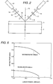
- a measuring optical system includes a pumping light source that emits pumping light 10 for changing the refractive index of the nonlinear optical thin film 3, a measuring light source 12 that emits a measuring optical signal 11, a collimator lens 14 for collimating scattering light rays emitted by the light source 12, a polarizer 16, a condenser lens 18, a condenser lens 19, an analyzer 17, a collimator lens 15 for collimating scattering light rays, and a light-receiving device 13 for receiving the measuring optical signal.
- Fig. 3 is a schematic view of a workpiece in different phases of an optical switch fabricating process.
- a SiO 2 is deposited in a 15 ⁇ m thick film by a flame hydrolysis deposition process to form the cladding 2 on the 1 mm thick substrate 4.
- a 6 ⁇ m thick composite oxide film of SiO 2 -TiO 2 is deposited by a flame hydrolysis deposition process over the 15 ⁇ m thick cladding 2 formed on the 1 mm thick substrate 4, and the composite oxide film is processed by a high-temperature treatment at 1000°C for densification.
- a mask covering a part, corresponding to the core 1 shown in Fig. 1, of the composite oxide film is formed over the composite oxide film by lithography, and parts of the composite oxide film not covered with the mask are removed by etching, and then the mask is removed to form the waveguide core 1 shown in Fig. 1.
- a 0.06 nm thick 95Co 3 O 4 film for forming the nonlinear thin film 3 is deposited on the surface of the core 1 by a sputtering process.
- a Cr electrode 8 is shown in Fig. 3(D), the Cr electrode 8 will be describe in connection with a second embodiment that uses the Cr electrode 8 because the Cr electrode 8 is irrelevant to the first embodiment.
- the optical characteristics of the nonlinear optical thin film 3 were examined.
- a test piece was prepared by forming only a test nonlinear optical thin film 3 on a substrate 4.
- S-polarized light beam and p-polarized light beam were used as the measuring optical signal 11.
- An optical system that measures refractive index by ellipsometry was used.
- the optical system determines the refractive index of the test nonlinear optical thin film 3 on the basis of the difference between the reflectivity of the nonlinear optical thin film 3 to the s-polarized light beam and that of the same to the p-polarized light beam.
- the respective wavelengths of the pumping light 10 and the measuring optical signal 11 are optionally changeable.
- a semiconductor laser having a maximum output capacity of 20 mW and capable of emitting a laser light beam of 650 nm in wavelength was used as a light source for emitting the pumping light 10.
- a laser normally used for communication and capable of emitting a light beam of 1550 nm in wavelength, and a semiconductor laser capable of emitting a light beam of 650 nm in wavelength, which is equal to the wavelength of the measuring optical signal 10, were used as light sources for emitting the measuring optical signal 11.
- the intensity of the measuring optical signal 11, as compared with that of the pumping light 10 was limited to a low level so that the test piece might not be pumped by the measuring optical signal 11.
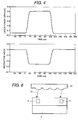
- Fig. 4 shows the variation of the refractive index of the test nonlinear optical thin film 3 with time when the test nonlinear optical thin film 3 was irradiated with the pumping light 10.
- the power of a pumping laser light pulse increased to a predetermined power level in about 12 ns after time when the pumping laser had been started.
- the refractive index of the test nonlinear optical thin film 3 decreased as the power of the pumping laser light pulse increased.
- Fig. 5 shows the dependence of the refractive index of the nonlinear optical thin film 3 on the power of the pumping light 10 by way of example.
- the maximum refractive index decreased gradually as the power of the pumping light 10, i.e., the laser light pulse, increased gradually.
- Refractive index was measured 12 ns after the power of the pumping light 10 had reached the predetermined level to determine the dependence of the refractive index on the power of the pumping light 10.
- the refractive index of the nonlinear optical thin film 3 was 3.2 for the measuring optical signal of 1550 nm in wavelength and 2.4 for the measuring optical signal of 650 nm in wavelength when the nonlinear optical thin film 3 was not irradiated with the pumping light 10.
- the refractive index of the nonlinear optical thin film 3 for either of the two measuring optical signals decreased as the power of the pumping light 10 increased.
- the refractive index of the nonlinear optical thin film was abput 3.1 for the measuring optical signal of 1550 nm in wavelength, and about 2.2 for the measuring optical signal of 650 nm in wavelength.
- the refractive index decreased further.
- the refractive index was about 3.1 for the measuring optical signal 11 of 1550 nm in wavelength, and 2.2 for the measuring optical signal 11 of 650 nm in wavelength.
- the quality of the nonlinear optical thin film was deteriorated by the pumping light 10 when the power of the pumping light 10 increased beyond 1.5 MW/cm 2 .
- the refractive index of the nonlinear optical thin film 3 changes when the nonlinear optical thin film 3 is irradiated with the pumping light 10 of 650 nm or above in wavelength.
- the nonlinear optical thin film 3 has a very high transmittance to light of 1550 nm in wavelength in a communication band and is capable of transmitting light with a low loss.
- the intensity of the pumping light 10, i.e., the laser beam was 1 MW/cm 2 or below, the quality of the nonlinear optical thin film was not deteriorated and the refractive index could be greatly changed.
- the power of the pumping light 10, i.e., the laser beam was 0.5 MW/cm 2 or below, the power consumption of an optical switch system including the optical switch could be reduced and the refractive index of the nonlinear optical thin film could be changed greatly for switching.
- Fig. 6 shows the optical switch combined with a surface laser 22 which emits pumping light 10.
- the branching point of each optical signal of the optical switch in the first embodiment was irradiated with the pumping light of 650 nm in wavelength emitted by the surface laser 22, and a change in the position of an output optical signal was measured.
- the nonlinear optical thin film 3 of the optical switch in the first embodiment was pumped by the pumping light 10 emitted by the surface laser 22.
- the optical switch exercised a similar switching effect also when the nonlinear optical thin film 3 was pumped by a multiple light beam produced by superposing the pumping light 10 on the incident light beam incident on the core a and when the nonlinear optical thin film 3 was pumped by only the pumping light 10 propagated through the waveguide.
- Fig. 7 is a table showing the results of examination of the characteristics of nonlinear optical materials suitable for forming the nonlinear optical thin films for optical switches according to the present invention.
- the nonlinear optical thin film of the optical switch in the first embodiment is formed of 95Co 3 O 4 .
- the performance of nonlinear optical thin films respectively formed of Sr 2 CoO 3 , Sr 2 FeO 3 , SrNiO 3 , Fe 3 O 4 , Co 3 O 4 , VO 2 , Dy 3 Fe 5 O 12 , ZnO and CoO was examined.
- Fig. 7 columns from the leftmost to the right are for nonlinear optical materials, extinction coefficients for a measuring optical signal of 1550 nm in wavelength, changes of refractive index for the measuring optical signal of 1550 nm in wavelength, intensities of an output optical signal from the optical switches corresponding to the first embodiment, switching performance and response speeds, respectively.
- the intensity of the output optical signal is represented by the ratio in percent of the intensity of the output optical signal to that of incident light, and switching characteristic is expressed by a double circle indicating satisfactory switching or a cross indicating unsatisfactory switching. All the nonlinear optical thin films excluding the nonlinear optical thin film formed of CoO were satisfactory in switching characteristic.
- An optical switch provided with a nonlinear optical thin film in a second embodiment according to the present invention is similar in construction as the optical switch in the first embodiment, except that the former is provided with a Cr electrode 8 as shown in Fig. 3(D) to apply a voltage across the nonlinear optical thin film.
- the optical switch in the second embodiment is a voltage-driven optical switch.
- a 150 nm thick ZnS film i.e., a light-emitting film, was formed on a cladding formed on a Si Substrate 4, and a 100 nm thick insulating film of SiO 2 was formed on the ZnS film.
- a 15 nm thick Cr film was formed on the insulating film, and a Cr electrode 8 was formed by subjecting the Cr film to photolithographic etching to complete an optical switch.
- the optical switch responded at a high response speed for high-speed switching.
- the optical switch in the third embodiment using fluorescent light as pumping light is capable of operating at low power consumption, of responding at a high response speed and of being miniaturized.
- the optical switch includes a waveguide core 1, a cladding 2, a nonlinear optical thin film 3, and a substrate 4.
- the core 1 is formed of a composite oxide, such as SiO 2 -TiO 2 prepared by mixing 1 mol % TiO 2 in SiO 2 .
- the cladding 2 is formed of SiO 2 .
- the substrate is a 3 mm square, 1 mm thick SiO 2 glass substrate.
- the nonlinear optical thin film 3 is formed of an amorphous metal containing 66 parts by mol Co, 12 parts by mol Cr, and 22 parts by mole Zr. Since the nonlinear optical thin film 3 is a metal thin film, an optical signal is reflected by the nonlinear optical thin film 3.
- a method of fabricating the optical switch in the fourth embodiment is the same as that of fabricating the optical switch in the first embodiment shown in Fig. 3, except that the nonlinear optical thin film 3, i.e., the metal thin film, is in contact with the core 1.
- nonlinear optical thin film 3 of the fourth embodiment was formed by cutting a metal thin film by an ion milling process
- an optical switch formed by forming a hole in the waveguide and inserting an amorphous metal thin film in the hole of the waveguide has the same effect as the optical switch in the fourth embodiment.
- Fig. 9 is a table showing the results of examination of the characteristics of nonlinear optical materials suitable for the optical switch in the fourth embodiment.
- Columns from the leftmost to the right are for nonlinear optical materials, reflectances for a measuring optical signal of 1550 nm in wavelength, changes of refractive index for the measuring optical signal of 1550 nm in wavelength, intensities of the output optical signal from the optical switches corresponding to the fourth embodiment, switching performance, and response speeds, respectively.
- the nonlinear optical thin film 3 of the optical switch in the fourth embodiment was formed of 66Co12Cr22Zr.
- Optical switches respectively having nonlinear optical thin films respectively formed of 66Ni12Cr22Zr, 66Fe12Cr22Zr, and a mixture of 66Co12Cr22Zr and 5% by mole of SiO 2 were tested. All the optical switches exhibited high-speed switching operation.
- the optical switch in the fourth embodiment is provided with the reflecting amorphous metal film as the nonlinear optical thin film 3.
- an optical switch in a fifth embodiment is provided with a nonlinear optical thin film 3 for converting a transmitted light beam into a reflected light beam.
- the optical switch in the fifth embodiment includes a waveguide core 1, a cladding 2, a nonlinear optical thin film 3, and a substrate 4 provided with a hole 5 of 1 mm in diameter for receiving the nonlinear optical thin film 3 therein.
- the nonlinear optical thin film 3 was formed of 95Co 3 O 4 in 60 nm in thickness on a glass plate of 1 mm in diameter and 1 mm in thickness, and the glass plate provided with the nonlinear optical thin film 3 was fitted in the hole 5 of the substrate 4.
- the dependence of the position of an output optical signal on pumping light 10 was examined.
- a laser beam of 650 nm in wavelength emitted by a surface laser was used as the pumping light 10 for irradiating the nonlinear optical thin film 3.
- the optical signal incident on a core a emerged from a core b .
- the optical signal incident on the core a emerged from a core c .
- Response speed of the optical switch measured by using a photodiode and an oscilloscope was 1 ns, which proved that the optical switch is capable of high-speed switching.
- nonlinear optical thin film 3 of the fifth embodiment was formed by cutting a metal thin film by an ion milling process
- an optical switch formed by forming a hole in the waveguide and inserting a nonlinear optical metal thin film 3 in the hole of the waveguide has the same effect as the optical switch in the fifth embodiment.
- the optical switch in the fifth embodiment is capable of achieving "transmitted light” ⁇ "reflected light” conversion.
- a thin film of NiO or Fe 3 O 4 may be used instead of the nonlinear optical thin film 3 of 95Co 3 O 4 .
- an optical switch in a sixth embodiment uses the optical switch in the third embodiment to convert transmitted light into reflected light.
- the optical switch in the sixth embodiment includes highly refractive substrates 6, and a nonlinear optical thin film 3.
- the substrates 6 are Si substrates having a refractive index of 3.4.
- the Si substrates 6 are processed in 75° to convert transmitted light into reflected light.
- the Si substrates 6 are fixedly held between and bonded with an adhesive, such as Araldite (trade name), to glass plates 8.
- the shape in plane of the highly refractive substrates 6 is not limited to a triangle and the substrates 6 may be formed in any suitable shape provided that incident light a, transmitted light c and reflected light b are able to fall, penetrate and leave the side surfaces of the highly refractive substrates 6 substantially perpendicularly.
- the respective apexes A and B of the triangular highly refractive substrates 6 shown in Fig. 11 may be rounded, may be formed in the shape of a circular or elliptic arc.
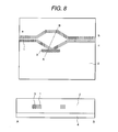
- a multichannel optical switch in a seventh embodiment is built by arranging optical switches similar to that in the fifth embodiment.
- the multichannel optical switch in the seventh embodiment includes cores 1, a cladding 2, thirteen nonlinear optical thin films 3, and holes 5 for accommodating the nonlinear optical thin films 3.
- the multichannel optical switch in the seventh embodiment has four light-receiving optical paths and four light-emitting optical paths.
- a process of fabricating the multichannel optical switch in the seventh embodiment is similar to that of fabricating the optical switch in the fifth embodiment.
- An optical signal falls on the left side, as viewed in Fig. 12, of the multichannel optical switch, and an output optical signal emerges from the right side, as viewed in Fig. 12, of the multichannel optical switch.
- a surface laser 22 is used for emitting pumping light beams 10.
- the nonlinear optical thin films 3 disposed at the intersections of the optical paths are irradiated with the pumping light beams 10 selectively; that is the pumping light 10 emitted by the surface laser 22 falls on the intersection point of each core. Timing of light emission by the surface laser 22 is determined on the basis of switching information included in an optical signal.
- the positional relation between the pumping light 10 and the output optical signal was examined by using the optical switch in the seventh embodiment.
- an optical signal was applied to the optical switch without irradiating the optical switch with the pumping light 10
- the optical signal incident on a core a emerged from a core b .
- an optical signal was applied to the optical switch while an X-1 of the optical switch was irradiated with the pumping light 10
- the optical signal incident on the core a emerged from a core c .
- the optical signal incident on the core a emerged from a core d .
- Fig. 13 is a table showing the results of examination of the characteristics of nonlinear optical materials suitable for forming the nonlinear optical thin films of the multichannel optical switch.
- columns from the leftmost to the right are for nonlinear optical materials, extinction coefficients for a measuring optical signal of 1550 nm in wavelength, changes of refractive index for the measuring optical signal of 1550 nm in wavelength, intensities of the output optical signal from the optical switches corresponding to the first embodiment, switching performance and response speeds, respectively.
- the characteristics of most of those nonlinear optical materials were satisfactory.
- a nonlinear optical thin film 3 formed of VO 2 had a large extinction coefficient of 0.16.
- Multichannel optical switches provided with nonlinear optical thin films of Co 3 O 4 and Fe 3 O 4 were capable of switching at a very high response speed of 1.2 ps.
- multichannel optical switch in the seventh embodiment is provided with optical switches similar to the optical switch in the fifth embodiment provided with the nonlinear optical thin film 3 accommodated in a hole formed in the substrate 4, multichannel optical switches provided with optical switches corresponding to the optical switches in the first to the fourth embodiment and the sixth embodiment demonstrated a high-speed optical signal switching capability.
- the multichannel optical switch in the seventh embodiment can be operated for the high-speed switching of a plurality optical channels by irradiating the nonlinear optical thin films 3 disposed at the intersections of the optical paths with the pumping light 10.
- the optical switch provided with the nonlinear optical thin film according to the present invention has an excellent response characteristic and is suitable for switching a large amount of information.
- the optical switch having at least one input core a , a plurality of output cores b and c , and a plurality of waveguides connecting the plurality of output cores b and c , and provided with the nonlinear optical thin film 3 capable of changing its refractive index by 2% or above relative to the surroundings to control the traveling direction of the optical signal and disposed near at least one of the plurality of waveguides, is capable of operating for high-speed switching at a response speed in the range of 10 ns to 1 ps. Since the optical switch is very small, an nxn matrix optical switch can be realized.
Landscapes
- Physics & Mathematics (AREA)
- Nonlinear Science (AREA)
- General Physics & Mathematics (AREA)
- Optics & Photonics (AREA)
- Optical Modulation, Optical Deflection, Nonlinear Optics, Optical Demodulation, Optical Logic Elements (AREA)
- Optical Integrated Circuits (AREA)
- Semiconductor Lasers (AREA)
Abstract
Description
Claims (13)
- An optical switch comprising:wherein a nonlinear optical element (3) which, when pumped, changes its refractive index by 2% or above relative to the surroundings to control a traveling direction of the optical signal is disposed near at least one of the plurality of waveguides.at least one light-receiving core (1, a) for receiving an optical signal;a plurality of light-emitting cores (1, b, c) which are used selectively for emitting the optical signal; anda plurality of waveguides (1) connecting the light-receiving core and the plurality of light-emitting cores;
- An optical switch comprising:wherein a nonlinear optical element (3) which, when pumped, changes its refractive index by 2% or above relative to the surroundings to control the reflection of the optical signal is disposed on a wall of at least one of the plurality of waveguides.at least one light-receiving core (1, a) for receiving an optical signal;a plurality of light-emitting cores (1, b, c) which are used selectively for emitting the optical signal; anda plurality of waveguides (1) connecting the light-receiving core and the plurality of light-emitting cores;
- An optical switch comprising:wherein a nonlinear optical element (3) which, when pumped, changes its refractive index by 2% or above relative to the surroundings to control the transmission/reflection of the optical signal is inserted in a hole (5) formed in the waveguide.at least one light-receiving core (1, a) for receiving an optical signal;a plurality of light-emitting cores (1, b, c) which are used selectively for emitting the optical signal; anda plurality of waveguides (1) connecting the light-receiving core and the plurality of light-emitting cores;
- An optical switch comprising:wherein a nonlinear optical element (3) which, when pumped, changes its refractive index by 2% or above relative to the surroundings to control the direction of the emitted optical signal is held between highly refractive substrates (6),at least one light-receiving core (1, a) for receiving an optical signal;a plurality of light-emitting cores (1, b, c) which are used selectively for emitting the optical signal; anda plurality of waveguides (1) connecting the light-receiving core and the plurality of light-emitting cores;
an optical signal fallen on one of the highly refractive substrates is emitted through the other highly refractive substrate when the nonlinear optical element is not pumped, and
an optical signal fallen on one of the highly refractive substrates is reflected by the same highly refractive substrate when the nonlinear optical element is pumped. - The optical switch according to any of claims 1 to 4, wherein the nonlinear optical element (3) and a substrate are stacked alternately to form an nxn matrix type optical switch.
- The optical switch according to any of claims 1 to 5 further comprising a pumping light source (12) for changing the refractive index of the nonlinear optical element (3).
- The optical switch according to any of claims 1 to 5 further comprising a pumping power source (8, 12) for changing the refractive index of the nonlinear optical element (3).
- The optical switch according to claim 6, wherein the pumping light source (12) has an output capacity of 1 MW/cm2 or below.
- The optical switch according to claim 7, wherein the pumping power source (8, 12) has an output capacity of 1 MW/cm2 or below.
- The optical switch according to any of claims 1 to 9, wherein the refractive index of the nonlinear optical element (3) has an extinction coefficient of 0.15% or below for a wavelength range of the optical signal.
- The optical switch according to any of claims 1 to 10, wherein the nonlinear optical element (3) has an energy gap corresponding to a wavelength in the range of 400 to 1200 nm.
- The optical switch according to any of claims 1 to 11, wherein the nonlinear optical element (3) is formed of an oxide of a metal selected from the group consisting of Co, Fe, Cr, Ni, V, Zn and Cu or a composite oxide containing the same metal oxide.
- The optical switch according to any of claims 1 to 12, wherein the nonlinear optical element (3) contains at least a metal selected from the group consisting of Co, Fe and Ni, and the metal is amorphous.
Applications Claiming Priority (2)
| Application Number | Priority Date | Filing Date | Title |
|---|---|---|---|
| JP2002025807 | 2002-02-01 | ||
| JP2002025807A JP2003228088A (en) | 2002-02-01 | 2002-02-01 | Light switch |
Publications (2)
| Publication Number | Publication Date |
|---|---|
| EP1333317A2 true EP1333317A2 (en) | 2003-08-06 |
| EP1333317A3 EP1333317A3 (en) | 2005-04-20 |
Family
ID=19192326
Family Applications (1)
| Application Number | Title | Priority Date | Filing Date |
|---|---|---|---|
| EP02015383A Withdrawn EP1333317A3 (en) | 2002-02-01 | 2002-07-10 | Nonlinear optical switch |
Country Status (5)
| Country | Link |
|---|---|
| US (1) | US6792167B2 (en) |
| EP (1) | EP1333317A3 (en) |
| JP (1) | JP2003228088A (en) |
| KR (1) | KR20030066290A (en) |
| TW (1) | TW583417B (en) |
Families Citing this family (6)
| Publication number | Priority date | Publication date | Assignee | Title |
|---|---|---|---|---|
| US6790502B1 (en) * | 1999-10-15 | 2004-09-14 | Hitachi, Ltd. | Optically functional element and production method and application therefor |
| JP2003295237A (en) * | 2002-03-29 | 2003-10-15 | Hitachi Ltd | Multi-division type optical switch |
| US6844092B2 (en) * | 2002-08-22 | 2005-01-18 | Hitachi, Ltd. | Optically functional element and production method and application therefor |
| KR100583436B1 (en) * | 2003-11-14 | 2006-05-26 | 한국과학기술연구원 | Waveguide Optical Device Using Giant Tertiary Nonlinear Optical Material and Its Operation Method |
| JP4279753B2 (en) | 2004-01-08 | 2009-06-17 | 株式会社日立製作所 | Optical information recording medium, manufacturing method thereof, and optical information recording / reproducing apparatus |
| JP2006276654A (en) | 2005-03-30 | 2006-10-12 | Hitachi Ltd | Optical switch and method of using the same |
Family Cites Families (16)
| Publication number | Priority date | Publication date | Assignee | Title |
|---|---|---|---|---|
| US4557551A (en) * | 1983-09-28 | 1985-12-10 | Andrew Corporation | Non-linear optical fiber coupler and a method of making same |
| GB8516108D0 (en) * | 1985-06-26 | 1985-07-31 | Gen Electric Co Plc | Optical switch |
| US5445767A (en) * | 1990-02-06 | 1995-08-29 | British Telecommunications Public Limited Company | Optical switches |
| US5136669A (en) * | 1991-03-15 | 1992-08-04 | Sperry Marine Inc. | Variable ratio fiber optic coupler optical signal processing element |
| JPH05196973A (en) * | 1991-09-12 | 1993-08-06 | Sumitomo Electric Ind Ltd | Optical switch |
| JPH05216079A (en) | 1992-02-05 | 1993-08-27 | Nippon Telegr & Teleph Corp <Ntt> | Waveguide type non-linear optical element and manufacturing method thereof |
| DE69311638T2 (en) * | 1992-07-15 | 1998-01-22 | Nippon Telegraph & Telephone | Optical switch |
| US6411591B1 (en) | 1997-09-18 | 2002-06-25 | Hitachi, Ltd. | Optical recording medium and optical memory device |
| JPH11337988A (en) | 1998-05-25 | 1999-12-10 | Asahi Glass Co Ltd | Light switch |
| US6081634A (en) * | 1998-09-25 | 2000-06-27 | The United States Of America As Represented By The National Security Agency | All-fiber optically-controlled optical switch |
| JP2001084643A (en) * | 1999-09-09 | 2001-03-30 | Hitachi Ltd | Optical disk media |
| EP1109049A1 (en) * | 1999-12-16 | 2001-06-20 | Corning Incorporated | Photothermal optical switch and variable attenuator |
| US6571028B1 (en) * | 2000-03-21 | 2003-05-27 | Evident Technologies | Optical switch having a saturable absorber |
| US6684003B2 (en) * | 2000-04-03 | 2004-01-27 | Massachusetts Institute Of Technology | All optical switch for optical integrated circuits |
| US6697542B2 (en) * | 2000-12-29 | 2004-02-24 | Lucent Technologies Inc. | Integrated optical switches using nonlinear optical media |
| GB0222062D0 (en) | 2002-09-23 | 2002-10-30 | British Telecomm | A data input device |
-
2002
- 2002-02-01 JP JP2002025807A patent/JP2003228088A/en active Pending
- 2002-07-02 TW TW091114661A patent/TW583417B/en not_active IP Right Cessation
- 2002-07-10 EP EP02015383A patent/EP1333317A3/en not_active Withdrawn
- 2002-08-23 US US10/226,309 patent/US6792167B2/en not_active Expired - Fee Related
- 2002-08-29 KR KR1020020051423A patent/KR20030066290A/en not_active Withdrawn
Also Published As
| Publication number | Publication date |
|---|---|
| JP2003228088A (en) | 2003-08-15 |
| US20030147584A1 (en) | 2003-08-07 |
| US6792167B2 (en) | 2004-09-14 |
| EP1333317A3 (en) | 2005-04-20 |
| TW583417B (en) | 2004-04-11 |
| KR20030066290A (en) | 2003-08-09 |
Similar Documents
| Publication | Publication Date | Title |
|---|---|---|
| JP3302458B2 (en) | Integrated optical device and manufacturing method | |
| CA2363630C (en) | Integrated optical switches using nonlinear optical mediums | |
| GB2177810A (en) | Optical switch | |
| KR100318041B1 (en) | Grating element, light wavelength selection utilizing the same, and optical signal transmitting system | |
| Moriyama et al. | Ultra-compact, self-holding asymmetric Mach-Zehnder interferometer switch using Ge2Sb2Te5 phase-change material | |
| US5483609A (en) | Optical device with mode absorbing films deposited on both sides of a waveguide | |
| US6792167B2 (en) | Optical switch | |
| JP2003279914A (en) | Tunable optical element | |
| CN115657218B (en) | Lens-assisted all-solid-state beam scanning system | |
| JP2004233485A (en) | Apparatus for providing delay difference between polarization components and polarization mode dispersion compensator | |
| US7949217B2 (en) | Selectively enhancing angular beam deflection | |
| JPH0766088B2 (en) | Optical waveguide device | |
| JP2008065030A (en) | Light control element and composite light control element | |
| US6870983B2 (en) | Optical switch, element therefor, and optical switching method | |
| TW557376B (en) | Wavelength division multiplex optical switch | |
| US6778726B2 (en) | Optical switch | |
| WO2001038922A2 (en) | Analog optical switch using an integrated mach-zehnder interferometer having a movable phase shifter | |
| US6647167B1 (en) | Solid state optical switch and router | |
| CN221782531U (en) | A dimmable light module and optical switch | |
| JPH10325910A (en) | Optical branching device | |
| JP2014085398A (en) | Optical modulator and optical deflector | |
| CN120652612B (en) | Two-dimensional grating coupler | |
| JP2006184758A (en) | Optical waveguide and optical waveguide module | |
| CN112230336A (en) | Random proportion optical splitter supporting multiple modes on chip | |
| JPH0764132A (en) | Two-dimensional optical switch array and its switching control method |
Legal Events
| Date | Code | Title | Description |
|---|---|---|---|
| PUAI | Public reference made under article 153(3) epc to a published international application that has entered the european phase |
Free format text: ORIGINAL CODE: 0009012 |
|
| AK | Designated contracting states |
Designated state(s): AT BE BG CH CY CZ DE DK EE ES FI FR GB GR IE IT LI LU MC NL PT SE SK TR |
|
| AX | Request for extension of the european patent |
Extension state: AL LT LV MK RO SI |
|
| PUAL | Search report despatched |
Free format text: ORIGINAL CODE: 0009013 |
|
| AK | Designated contracting states |
Kind code of ref document: A3 Designated state(s): AT BE BG CH CY CZ DE DK EE ES FI FR GB GR IE IT LI LU MC NL PT SE SK TR |
|
| AX | Request for extension of the european patent |
Extension state: AL LT LV MK RO SI |
|
| RIC1 | Information provided on ipc code assigned before grant |
Ipc: 7G 02F 1/313 B Ipc: 7G 02F 1/35 A |
|
| 17P | Request for examination filed |
Effective date: 20051013 |
|
| AKX | Designation fees paid |
Designated state(s): DE FR GB NL |
|
| STAA | Information on the status of an ep patent application or granted ep patent |
Free format text: STATUS: THE APPLICATION HAS BEEN WITHDRAWN |
|
| 18W | Application withdrawn |
Effective date: 20070718 |