EP1331775A1 - Physical layer circuit and interface circuit - Google Patents
Physical layer circuit and interface circuit Download PDFInfo
- Publication number
- EP1331775A1 EP1331775A1 EP02090038A EP02090038A EP1331775A1 EP 1331775 A1 EP1331775 A1 EP 1331775A1 EP 02090038 A EP02090038 A EP 02090038A EP 02090038 A EP02090038 A EP 02090038A EP 1331775 A1 EP1331775 A1 EP 1331775A1
- Authority
- EP
- European Patent Office
- Prior art keywords
- physical layer
- layer circuit
- bridge
- bus
- packets
- Prior art date
- Legal status (The legal status is an assumption and is not a legal conclusion. Google has not performed a legal analysis and makes no representation as to the accuracy of the status listed.)
- Withdrawn
Links
- 230000003139 buffering effect Effects 0.000 claims abstract description 12
- 238000004891 communication Methods 0.000 claims description 22
- 238000003780 insertion Methods 0.000 claims description 4
- 230000037431 insertion Effects 0.000 claims description 4
- 238000010586 diagram Methods 0.000 description 4
- 238000000034 method Methods 0.000 description 3
- 230000004048 modification Effects 0.000 description 3
- 238000012986 modification Methods 0.000 description 3
- 230000008569 process Effects 0.000 description 3
- 230000008901 benefit Effects 0.000 description 2
- 230000005540 biological transmission Effects 0.000 description 2
- 238000002955 isolation Methods 0.000 description 2
- 230000008859 change Effects 0.000 description 1
- 230000001419 dependent effect Effects 0.000 description 1
- 238000013461 design Methods 0.000 description 1
- 230000006870 function Effects 0.000 description 1
- 238000011900 installation process Methods 0.000 description 1
- 238000004519 manufacturing process Methods 0.000 description 1
Images

Classifications
-
- H—ELECTRICITY
- H04—ELECTRIC COMMUNICATION TECHNIQUE
- H04L—TRANSMISSION OF DIGITAL INFORMATION, e.g. TELEGRAPHIC COMMUNICATION
- H04L12/00—Data switching networks
- H04L12/28—Data switching networks characterised by path configuration, e.g. LAN [Local Area Networks] or WAN [Wide Area Networks]
- H04L12/40—Bus networks
- H04L12/40052—High-speed IEEE 1394 serial bus
- H04L12/40078—Bus configuration
-
- H—ELECTRICITY
- H04—ELECTRIC COMMUNICATION TECHNIQUE
- H04L—TRANSMISSION OF DIGITAL INFORMATION, e.g. TELEGRAPHIC COMMUNICATION
- H04L69/00—Network arrangements, protocols or services independent of the application payload and not provided for in the other groups of this subclass
- H04L69/30—Definitions, standards or architectural aspects of layered protocol stacks
- H04L69/32—Architecture of open systems interconnection [OSI] 7-layer type protocol stacks, e.g. the interfaces between the data link level and the physical level
-
- H—ELECTRICITY
- H04—ELECTRIC COMMUNICATION TECHNIQUE
- H04L—TRANSMISSION OF DIGITAL INFORMATION, e.g. TELEGRAPHIC COMMUNICATION
- H04L12/00—Data switching networks
- H04L12/28—Data switching networks characterised by path configuration, e.g. LAN [Local Area Networks] or WAN [Wide Area Networks]
- H04L12/40—Bus networks
- H04L12/40052—High-speed IEEE 1394 serial bus
-
- H—ELECTRICITY
- H04—ELECTRIC COMMUNICATION TECHNIQUE
- H04L—TRANSMISSION OF DIGITAL INFORMATION, e.g. TELEGRAPHIC COMMUNICATION
- H04L12/00—Data switching networks
- H04L12/28—Data switching networks characterised by path configuration, e.g. LAN [Local Area Networks] or WAN [Wide Area Networks]
- H04L12/40—Bus networks
- H04L12/40052—High-speed IEEE 1394 serial bus
- H04L12/40091—Bus bridging
-
- H—ELECTRICITY
- H04—ELECTRIC COMMUNICATION TECHNIQUE
- H04L—TRANSMISSION OF DIGITAL INFORMATION, e.g. TELEGRAPHIC COMMUNICATION
- H04L12/00—Data switching networks
- H04L12/64—Hybrid switching systems
Definitions
- the invention relates to a physical layer circuit for an interface circuit to a first communication bus and to an interface circuit.
- the IEEE1394 bus has become an important communication bus in the field of home systems.
- the IEEE1394 serial bus already provides an internationally standardized and very widely accepted bus for data exchange between terminals from both, the consumer electronics field, the precise designation of the afore mentioned standard is: IEEE standard for high performance serial bus, (IEEE) STD 1394-1995, IEEE New York, August 1996. In the year 2000 an improved version had been finalized with the reference IEEE1394a-2000.
- the IEEE1394 bus is a wired bus and it is specified that a maximum of 63 stations can participate in the communication over the bus lines.
- the 63 stations can be distributed in an apartment or a house.
- the maximum distance between two stations is 4.5 m, however there are also existing solutions that overcome the distance limitation.
- a problem with all wired bus systems is that a bus cable needs to be installed in every room where a bus station shall be located. This problematic gave rise to the wish of a wireless extension of the IEEE1394 standard.
- a stand-alone device or a cluster of devices shall communicate with a first cluster by means of a wireless link or bridge.
- BRAN Broadband Radio Access Networks
- SSCS Packet Based Convergence Layer
- SSCS Service Specification Convergence Sublayer
- the box that connects the 1394 bus cable of a cluster to the wireless bridge needs to have a standard conform 1394 interface but on the other hand it needs to have some additional functionality, which concerns the self- configuration phase of the network.
- the 1394 bus has life insertion capability and each time a device is added or removed from the bus a bus reset is performed. After a bus reset each bus node sends a self-ID packet to the bus, with which all other stations on the bus become aware of how many stations are present on the bus.
- the ID number is a 6-bit number so that 64 devices can be distinguished.
- There is a specific process defined in the 1394 standard with which the ID numbers are assigned to the stations. This will be described in more detail later on.
- the devices of the second cluster are not aware that they are connected via a wireless link to the network. To achieve transparent operation, it is necessary that the wireless boxes shall generate self-ID packets that reflect the topology on both buses.
- the physical layer circuit of the 1394 interface circuit for the boxes of the wireless bridge need to have an additional buffer memory in which the self-ID packet of the bus stations in the cluster, to which the wireless box is not connected, may be buffered. There is a process that transfers the self-ID packets of the bus stations in the cluster on the other side of the bridge over the wireless link after each bus reset.
- a bottleneck of this solution is that different physical layer circuits need to be used in the boxes of the wireless link than in all the other bus stations of both clusters.
- a physical layer circuit that includes the necessary buffer memory for the bridge functionality but also comprises configuration means that enable to either configure the physical layer circuit as a bridge portal physical layer circuit supporting the bridge functionality or else to configure the physical layer circuit as a standard physical layer circuit that has the buffering of self-ID packets in the buffer memory disabled.
- This solution has the advantage that one type of physical layer circuit can be used in different types of bus stations, namely bridge portal bus stations or non-bridge portal bus stations.
- the configuration means may consist of a configuration register in the physical layer circuit that has one or more register places dedicated to the enabling or disabling of the node-ID packet buffering, i.e. bridge functionality. This has the advantage that the configuration could be performed simply with software means performing a write access to the configuration register during an installation process in the assembly line.
- the physical layer circuit could have a pin connected with the configuration register. In this case it is possible to automatically configure the physical layer circuit after power on. Of course the corresponding potential high or low needs to be applied to the pin. Thus making the configuration by software means unnecessary.
- this pin is positioned at a place where a standard physical layer circuit that does not support the bridge functionality has a power supply pin ground or voltage supply.
- a standard physical layer circuit that does not support the bridge functionality has a power supply pin ground or voltage supply.
- the low/high value should be copied into the configuration register and when read out must be interpreted that the bridge functionality is switched off.
- a physical layer circuit for a communication bus has a plurality of ground/voltage supply pins so that taking away one of these pins would not cause a great problem for the chip design.
- a physical layer chip for an IEEE1394 interface has more than one port to connect the bus cable. It is then advantageous that in an interface device that includes such a physical layer circuit one of these ports remains unused, i.e. it is not connected to a corresponding socket for a bus cable. This avoids problems during the self-configuration phase of the whole network. If this measure would not have been taken the bus topology could not correctly be reproduced because then the bus topology of only one cluster would be reflected during the self-configuration phase.
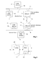
- Figure 1 shows two 1394 buses with 1394 bus stations and a wireless bridge in-between.
- the first 1394 bus has assigned reference number 7.
- a first and second 1394 device is shown with reference numbers 1 and 2.
- Such a device can be a consumer electronics device such as TV set, VCR, Camcorder, Set Top Box, DVD player, etc. or a computer device like PC, Notebook, etc.
- Each of these devices is a standard conform 1394 device and has a corresponding 1394 interface 10.
- Transceiver box 3 further has another interface 12 for wireless transmission. There are wireless protocols already existing supporting high-speed communication. As an example the Hiperlan system is mentioned.
- the document 'Broadband Radio Access Networks (BRAN); Hiperlan/2; Packet based convergence layer; Part 3: IEEE1394 Service Specific Convergence Sublayer (SSCS)" defines a sublayer emulating the IEEE1394 link layer over a ETSI BRAN Hiperlan/2 wireless network.
- BRAN Broadband Radio Access Networks
- SSCS Packet based convergence layer
- Other examples of wireless communication protocols for the wireless link are the IEEE 802.11 system, the Bluetooth system and the DECT system.
- FIG. 1 There is another cluster of 1394 devices shown in Fig. 1 having its own 1394 bus 8. Again, two 1394 devices 4 and 5 are depicted having standard 1394 interfaces 10.
- a second box 6 for the wireless bridge 9 is connected to the bus 8 as well.
- the total amount of bus stations in both clusters together inclusive wireless transceiver boxes 3 and 6 is less than or equal to 63. This is because with the wireless bridge 9 both clusters are merged together and data communication between devices from different clusters is from the point of view of the 1394 devices by no means different than for communication between devices in one cluster.
- the maximum allowed number of bus nodes in a 1394 cluster is however 63.
- the bus where a transceiver box of a wireless bridge has become the root device will be the remote bus. If in both buses a transceiver box of a wireless bridge has become the root device, a decision has to be made for example by game of dice.
- a scenario with only one 1394 device in the remote cluster is described in the European Patent Application 00 402 901.3.
- a scenario with more than one 1394 device in the remote cluster is described in the European Patent Application 01 400 826.2.
- Fig. 2 shows the principal structure of a 1394 interface 10 or 11.
- the 1394 interface is subdivided in two parts, a physical layer section 21 and a data link layer section 20. Both can be integrated in one single chip or two distinct chips.
- the data link layer section is implemented in software running on a powerful micro controller.
- the modified 1394 interface 11 has the same principle structure.
- the modification concerns a specific buffer memory 22 in the physical layer section and its management means. They are explained in detail in the European Patent Application 01 250 155.7. For the disclosure of the present invention it is therefore expressively referred also to this application.
- a bus reset is performed each time a 1394 device is plugged off (disconnected) from or plugged in (connected) to the bus.
- the 1394 bus standard provides full live insertion capability. An insertion or removal of a bus station is accompanied by a specific voltage change on the bus lines that is detected by electronic means providing the bus reset.
- a self-configuration phase follows for the network. During the self-configuration phase each bus station sends its self-ID packet to the bus to inform every other station in the network that it exists.
- a self-ID packet has the format of that in Fig. 3. It consists of 64 bits where the last 32 bits are the inverse of the first 32 bits. Of course all bits of the self-ID packets are explained in the 1394 standard itself. Some of them will be expressively explained here.
- At the beginning of a self-ID packet there is the physical ID-number of the bus station. This field has a length of 6 bits corresponding to the numbers 0 ... 63.
- At the end of the self-ID packets there are 2-bit fields for the ports P0 to P2 of a bus station. With the two bits it can be notified not only the existence of the port in the station but also whether the port is active and connected to a parent or child in the bus topology.
- a bus station can be equipped with up to 16 ports. If a station has more than 3 ports their status will be reported in a second or third self-ID packet. The last bit m in the self-ID packet has the function to indicate whether a second or third self-id packet will be send. In these self-id packets the status of the ports of the 1394 device will be reported.
- the bus is granted to the stations in a deterministic manner depending on the bus topology (in particular whether a station is branch or leaf).
- the physical ID number is assigned to the stations in the order of bus grant beginning from Zero. For addressing a data packet not only the physical ID-number (node-ID) is used. Each bus also has a bus-ID, which also needs to be taken into account during addressing.
- a number of problems occur during self-configuration after a bus reset.
- the devices are not aware that they are connected via a wireless link to the network.
- the bridge makes a bus reset isolation.
- the self-ID packets need to be forwarded from one cluster to the other via the wireless link.
- the reset is detected by all stations 1, 2, 3 in the cluster. After the bus reset the stations will send their self-ID packets one after the other. Each station in the cluster will collect the corresponding information in a higher software layer, e.g. in the transaction layer in order to be able to generate the right addresses later on.
- the interface 11 in the transceiver box 3 also receives each self-ID packet and forwards them via the wireless link to the second transceiver box 6. Also the box 3 generates a self-ID packet and sends it to the 1394 bus 7.
- wireless transceiver box 3 operates in legacy mode and generates a self-ID packet without taking into account that in case that the bridge is replaced by a 1394 cable, it would have a different physical ID number.
- the box 3 After having collected all self-ID packets from the cluster bus, the box 3 initiates a bus reset on the cluster bus by software means. Again the self-ID packets are transmitted over the bus. The difference is that when it is the turn of the box 3 to send its self-ID packet, it will generate not only its own self-ID packet but also all the self-ID packets of the stations in the remote cluster, whereby the box 3 generates the self-ID packets under consideration of the topology, which would result if the wireless link would be replaced by a 1394 cable. In the following the self-ID packets generated by the box 3 in representation of the stations in the cluster bus are called artificial self-ID packets.
- a bus reset is also initiated on the remote bus 8 by software means in box 6.
- the box 6 has collected all self-ID packets from the cluster bus and generates the corresponding artificial self-ID packets in this phase. After this phase the self-configuration is finalised and normal data communication can continue.
- the Physical Layer chip in the interfaces 11 of the wireless transceiver box 3 and 6 generate self-ID packets that are reflecting the topology on both buses.
- a specific buffer memory 22 in the physical layer circuit which can be a register bank or RAM.
- the physical layer circuit which can be a register bank or RAM.
- the information of the first quadlet of each self-ID packet will be stored in this register bank.
- the second quadlet of each self-ID packet will be created on-the-fly by the physical layer circuit itself (logical inverse of the first quadlet).
- the number of self-ID packets per node is dependent on the implemented ports per node.
- the micro controller of the wireless link will provide the information of the artificial self-ID packets. This information is stored in the buffer memory of the physical layer circuit.
- Fig. 4 shows a block diagram of a hard disk drive.
- the three main parts of the hard disk drive are the hard disk drive 15, a micro controller 14 and IEEE1394 interface 10. From these components only the interface 10 is shown in greater detail.
- the illustration again shows that the interface circuit 10 comprises the two main blocks physical layer circuit 21 and data link layer circuit 20. From the physical layer circuit 21 the three 1394 ports 23, the buffer memory 22 and a configuration register 24 are separately shown.
- the hard disk drive is configured as a standard 1394 bus station. In this case the entry in the configuration register 24 is 0, which means that the physical layer circuit 21 does not support the bridge functionality and, therefore makes no use of buffer memory 22 for buffering self-ID packets that have been received via the wireless bridge 9 from the remote bus.
- the configuration of physical layer circuit 21 with the configuration register 24 is that the physical layer circuit 21 does not have the additional bridge functionality, which especially means that the buffer memory 22 is not used to store any self-ID packets.
- Fig. 5 shows a wireless box of the wireless link 9 in block diagram from.
- This box also consists of three main parts.
- Reference number 13 denotes a micro controller
- reference number 11 denotes a 1394 bus interface
- reference number 12 denotes a Hiperlan/2 interface.
- the Hiperlan/2 interface is connected with a receiving and transmission antenna as shown in Fig. 5.
- this interface circuit 11 consists of the two main parts physical layer 21 and data link layer circuit 20.
- the entry in the configuration register 24 is 1, which means that the physical layer circuit 21 has bridge functionality and, therefore uses buffer memory 22 for buffering self-ID packets that have been received via the wireless bridge 9 from the remote bus.
- the occupied port 23 can be regarded as a virtual port over which the communication to the counter part of the wireless box namely wireless box 6 will take place.
- the communication to the wireless box 6 will not physically take place over this unoccupied port 23.
- the data that needs to be transferred to this box and will be received from this box have to be reformatted in a higher layer, e.g. application layer where they can be shifted to the Hiperlan/2 interface 12 and then they will be communicated to the other side with the specified Hiperlan/2 protocol.
- the virtual port is necessary so that the physical layer circuit 21 will generate the correct self-ID packets after the bus reset taking into account that behind the wireless bridge there are some more devices connected to the 1394 bus over the virtual port.
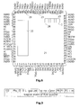
- Fig. 6 the pin assignments of a physical layer circuit according to the invention are shown. These pin assignments are identical to an existing physical layer IC from Texas Instruments named TSB41LV03A, except for one pin. This pin that is modified is the pin with the number 36. In the existing Texas Instruments IC this pin is also a ground pin named AGND like the four pins above pin 36.
- the physical layer circuit according to the invention has at this place a so-called configuration pin CON. This pin, therefore, is not being connected with the analogue ground of the IC. It is instead connected with a read/write register 24. It is sufficient that the pin is connected to only one register place of the read/write register 24.
- the configuration pin of the physical layer circuit can be an extra pin that is not used when the physical layer circuit is integrated in a standard IEEE1394 bus interface not having bridge functionality.
- the number of ports for bus cables need not be all connected with corresponding sockets. In one 1394 device more of the ports could be connected with corresponding sockets than in the other depending on the application.
- the writing into the configuration register 24 could be done in asynchronous fashion automatically by hardware after power-on of the physical layer circuit. Many different hardware implementations can be used for this.
- the bridge does not necessarily need to be a wireless bridge and especially not necessarily be a Hiperlan/2 bridge.
- the communication bus does not necessarily be an IEEE1394 bus.
Landscapes
- Engineering & Computer Science (AREA)
- Computer Networks & Wireless Communication (AREA)
- Signal Processing (AREA)
- Computer Security & Cryptography (AREA)
- Small-Scale Networks (AREA)
Abstract
The invention deals with a physical layer circuit (21) for
the IEEE1394 bus. Considered is a scenario where two
clusters of 1394 devices are linked to each other by means
of a wireless bridge (9). The devices of one cluster shall
communicate with devices of the other cluster without being
bridge aware. Under this scenario there are two different
types of 1394 devices existing in each cluster. One device
is a bridge portal and will have the bridge functionality.
All the other 1394 devices in the cluster will not have the
bridge functionality. As the device having the bridge
functionality needs to have a specific buffer memory (22)
for buffering node-ID packets, usually there are two
different types of physical layer circuits required for the
different types of 1394 devices. The invention deals with
the problem of how it can be realized to use in both
different types of 1394 devices the same type of physical
layer circuit (21). The invention solves the problem by
means of configuration means (24) in the physical layer
circuit (21). These configuration means enable either to
configure the physical layer circuit (21) as a bridge portal
physical layer circuit supporting the bridge functionality
by buffering said node-ID packets in said buffer memory (22)
or else configuring the physical layer circuit (21) as a
standard physical layer circuit that disables the buffering
of said node-ID packets. The new type of physical layer
circuit is pin compatible with a standard physical layer
circuit.
Description
The invention relates to a physical layer circuit for an
interface circuit to a first communication bus and to an
interface circuit.
The IEEE1394 bus has become an important communication bus
in the field of home systems. The IEEE1394 serial bus
already provides an internationally standardized and very
widely accepted bus for data exchange between terminals from
both, the consumer electronics field, the precise
designation of the afore mentioned standard is: IEEE
standard for high performance serial bus, (IEEE) STD 1394-1995,
IEEE New York, August 1996. In the year 2000 an
improved version had been finalized with the reference
IEEE1394a-2000.
The IEEE1394 bus is a wired bus and it is specified that a
maximum of 63 stations can participate in the communication
over the bus lines. The 63 stations can be distributed in an
apartment or a house. The maximum distance between two
stations is 4.5 m, however there are also existing solutions
that overcome the distance limitation.
A problem with all wired bus systems is that a bus cable
needs to be installed in every room where a bus station
shall be located. This problematic gave rise to the wish of
a wireless extension of the IEEE1394 standard. A stand-alone
device or a cluster of devices shall communicate with a
first cluster by means of a wireless link or bridge.
Today, wireless communication systems already exist that can
be used for the wireless link/bridge. The document
"Broadband Radio Access Networks (BRAN; Hiperlan/2; Packet
Based Convergence Layer; Part 3: IEEE1394 Service
Specification Convergence Sublayer (SSCS)" defines a
sublayer emulating the IEEE link layer over an ETSI BRAN
Hiperlan/2 wireless network. As such, it may be present in
bridge devices between wired 1394 buses or in stand-alone
wireless devices.
The inter-connection of the different buses (with different
bus-ID's) involves an IEEE1394 bridge, which is currently
under definition by the IEEE P1394.1 working group. Because
of the use of different bus-IDs an application operating on
bridges shall be bridge aware.
The box that connects the 1394 bus cable of a cluster to the
wireless bridge needs to have a standard conform 1394 interface
but on the other hand it needs to have some additional
functionality, which concerns the self- configuration phase
of the network. The 1394 bus has life insertion capability
and each time a device is added or removed from the bus a
bus reset is performed. After a bus reset each bus node
sends a self-ID packet to the bus, with which all other
stations on the bus become aware of how many stations are
present on the bus. The ID number is a 6-bit number so that
64 devices can be distinguished. There is a specific process
defined in the 1394 standard, with which the ID numbers are
assigned to the stations. This will be described in more
detail later on.
For now it is sufficient to explain that this process will
be done separately for both clusters that are connected
through the wireless bridge. This is because the wireless
bridge makes a bus reset isolation between both clusters.
This is a problem and the customer would not accept a
limitation in the control of bus stations due to the
existence of two or more 1394 clusters in his home. The
customer, therefore, wants to have a network topology being
displayed in the form of one single cluster to be able to
easily control the various devices from different locations.
There is, therefore, the desire that all the stations in the
network shall be configured as belonging to one 1394 bus and
this calls for a modified self-configuration phase that must
be performed in co-ordinated fashion in both clusters with
the bridge circuit in-between.
The devices of the second cluster are not aware that they
are connected via a wireless link to the network. To achieve
transparent operation, it is necessary that the wireless
boxes shall generate self-ID packets that reflect the
topology on both buses.
A solution for this problem is already presented in the
European Patent Application 01 250 155.7 of the applicant.
According to this solution, the physical layer circuit of
the 1394 interface circuit for the boxes of the wireless
bridge need to have an additional buffer memory in which the
self-ID packet of the bus stations in the cluster, to which
the wireless box is not connected, may be buffered. There is
a process that transfers the self-ID packets of the bus
stations in the cluster on the other side of the bridge over
the wireless link after each bus reset.
A bottleneck of this solution is that different physical
layer circuits need to be used in the boxes of the wireless
link than in all the other bus stations of both clusters.
From the demands of modern production lines, it would be
advantageous if the same physical layer circuit could be
used in both types of bus stations regardless of whether
they are part of the wireless link or not.
It is an object of the invention to provide a physical layer
circuit for a communication bus that can be used in both
types of bus stations, bridge portal box or out of bridge
bus station.
This objective is achieved by a physical layer circuit that
includes the necessary buffer memory for the bridge
functionality but also comprises configuration means that
enable to either configure the physical layer circuit as a
bridge portal physical layer circuit supporting the bridge
functionality or else to configure the physical layer
circuit as a standard physical layer circuit that has the
buffering of self-ID packets in the buffer memory disabled.
This solution has the advantage that one type of physical
layer circuit can be used in different types of bus
stations, namely bridge portal bus stations or non-bridge
portal bus stations.
Further improvements of the physical layer circuit are
possible by virtue of the measures evinced in the dependant
claims. The configuration means may consist of a configuration
register in the physical layer circuit that has one
or more register places dedicated to the enabling or
disabling of the node-ID packet buffering, i.e. bridge
functionality. This has the advantage that the configuration
could be performed simply with software means performing a
write access to the configuration register during an
installation process in the assembly line.
The physical layer circuit could have a pin connected with
the configuration register. In this case it is possible to
automatically configure the physical layer circuit after
power on. Of course the corresponding potential high or low
needs to be applied to the pin. Thus making the
configuration by software means unnecessary.
Preferably, this pin is positioned at a place where a
standard physical layer circuit that does not support the
bridge functionality has a power supply pin ground or
voltage supply. This means that the configuration pin would
be pulled to low/high potential in an interface circuit for
a standard bus station. The low/high value should be copied
into the configuration register and when read out must be
interpreted that the bridge functionality is switched off.
Typically a physical layer circuit for a communication bus
has a plurality of ground/voltage supply pins so that taking
away one of these pins would not cause a great problem for
the chip design.
Typically a physical layer chip for an IEEE1394 interface
has more than one port to connect the bus cable. It is then
advantageous that in an interface device that includes such
a physical layer circuit one of these ports remains unused,
i.e. it is not connected to a corresponding socket for a bus
cable. This avoids problems during the self-configuration
phase of the whole network. If this measure would not have
been taken the bus topology could not correctly be
reproduced because then the bus topology of only one cluster
would be reflected during the self-configuration phase.
Exemplary embodiments of the invention are illustrated in
the drawings and are explained in more detail in the
following description.
In the figures:
- Fig. 1
- shows two 1394 clusters connected to each other via a wireless bridge;
- Fig. 2
- shows a block diagram of a 1394 bus interface circuit;
- Fig. 3
- shows the format of a self-ID packet;
- Fig. 4
- shows a block diagram of a standard bus station not having the bridge functionality activated;
- Fig. 5
- shows a wireless box of a wireless link which is a bus station having the bridge functionality activated, and
- Fig. 6
- shows the pin assignments of a physical layer circuit according to the circuit.
Figure 1 shows two 1394 buses with 1394 bus stations and a
wireless bridge in-between. The first 1394 bus has assigned
reference number 7. A first and second 1394 device is shown
with reference numbers 1 and 2. Such a device can be a
consumer electronics device such as TV set, VCR, Camcorder,
Set Top Box, DVD player, etc. or a computer device like PC,
Notebook, etc. Each of these devices is a standard conform
1394 device and has a corresponding 1394 interface 10.
With reference number 3 a first transceiver box for the
wireless link 9 is denoted. This box also needs to have a
1394 interface because it is also connected to the 1394 bus
lines 7. The corresponding interface has reference number 11
in Fig. 1. This indicates already that it is not the same
1394 interface as that of devices 1 and 2. 1394 interface 11
has additional functionality involving the invention.
Transceiver box 3 further has another interface 12 for
wireless transmission. There are wireless protocols already
existing supporting high-speed communication. As an example
the Hiperlan system is mentioned. The document 'Broadband
Radio Access Networks (BRAN); Hiperlan/2; Packet based
convergence layer; Part 3: IEEE1394 Service Specific
Convergence Sublayer (SSCS)" defines a sublayer emulating
the IEEE1394 link layer over a ETSI BRAN Hiperlan/2 wireless
network. Other examples of wireless communication protocols
for the wireless link are the IEEE 802.11 system, the
Bluetooth system and the DECT system.
There is another cluster of 1394 devices shown in Fig. 1
having its own 1394 bus 8. Again, two 1394 devices 4 and 5
are depicted having standard 1394 interfaces 10. A second
box 6 for the wireless bridge 9 is connected to the bus 8 as
well. For the conception of the invention it is required
that the total amount of bus stations in both clusters
together inclusive wireless transceiver boxes 3 and 6 is
less than or equal to 63. This is because with the wireless
bridge 9 both clusters are merged together and data
communication between devices from different clusters is
from the point of view of the 1394 devices by no means
different than for communication between devices in one
cluster. The maximum allowed number of bus nodes in a 1394
cluster is however 63. It is defined that the bus where a
transceiver box of a wireless bridge has become the root
device will be the remote bus. If in both buses a
transceiver box of a wireless bridge has become the root
device, a decision has to be made for example by game of
dice.
A scenario with only one 1394 device in the remote cluster
is described in the European Patent Application 00 402
901.3. A scenario with more than one 1394 device in the
remote cluster is described in the European Patent
Application 01 400 826.2.
Fig. 2 shows the principal structure of a 1394 interface 10
or 11. The 1394 interface is subdivided in two parts, a
physical layer section 21 and a data link layer section 20.
Both can be integrated in one single chip or two distinct
chips. In principle it would also be possible that the data
link layer section is implemented in software running on a
powerful micro controller. Also the modified 1394 interface
11 has the same principle structure. The modification
concerns a specific buffer memory 22 in the physical layer
section and its management means. They are explained in
detail in the European Patent Application 01 250 155.7. For
the disclosure of the present invention it is therefore
expressively referred also to this application.
To understand the modification of the physical layer chip it
is helpful to first explain what happens in case of a bus
reset. A bus reset is performed each time a 1394 device is
plugged off (disconnected) from or plugged in (connected) to
the bus. The 1394 bus standard provides full live insertion
capability. An insertion or removal of a bus station is
accompanied by a specific voltage change on the bus lines
that is detected by electronic means providing the bus
reset. After a bus reset a self-configuration phase follows
for the network. During the self-configuration phase each
bus station sends its self-ID packet to the bus to inform
every other station in the network that it exists.
A self-ID packet has the format of that in Fig. 3. It
consists of 64 bits where the last 32 bits are the inverse
of the first 32 bits. Of course all bits of the self-ID
packets are explained in the 1394 standard itself. Some of
them will be expressively explained here. At the beginning
of a self-ID packet there is the physical ID-number of the
bus station. This field has a length of 6 bits corresponding
to the numbers 0 ... 63. At the end of the self-ID packets
there are 2-bit fields for the ports P0 to P2 of a bus
station. With the two bits it can be notified not only the
existence of the port in the station but also whether the
port is active and connected to a parent or child in the bus
topology. According to the IEEE1394 bus standard a bus
station can be equipped with up to 16 ports. If a station
has more than 3 ports their status will be reported in a
second or third self-ID packet. The last bit m in the self-ID
packet has the function to indicate whether a second or
third self-id packet will be send. In these self-id packets
the status of the ports of the 1394 device will be reported.
With the 1394 bus data communication in half-duplex
operation mode is possible. Therefore, only one station is
sending data to the bus and the rest is listening. The bus
is granted to the stations in a deterministic manner
depending on the bus topology (in particular whether a
station is branch or leaf). The physical ID number is
assigned to the stations in the order of bus grant beginning
from Zero. For addressing a data packet not only the
physical ID-number (node-ID) is used. Each bus also has a
bus-ID, which also needs to be taken into account during
addressing.
In case of the bus structure shown in Fig. 1 a number of
problems occur during self-configuration after a bus reset.
The devices are not aware that they are connected via a
wireless link to the network. The bridge makes a bus reset
isolation. The self-ID packets need to be forwarded from one
cluster to the other via the wireless link.
Now it is considered that a bus reset happened in the
cluster bus 7. The reset is detected by all stations 1, 2, 3
in the cluster. After the bus reset the stations will send
their self-ID packets one after the other. Each station in
the cluster will collect the corresponding information in a
higher software layer, e.g. in the transaction layer in
order to be able to generate the right addresses later on.
The interface 11 in the transceiver box 3 also receives each
self-ID packet and forwards them via the wireless link to
the second transceiver box 6. Also the box 3 generates a
self-ID packet and sends it to the 1394 bus 7. In the first
attempt wireless transceiver box 3 operates in legacy mode
and generates a self-ID packet without taking into account
that in case that the bridge is replaced by a 1394 cable, it
would have a different physical ID number.
After having collected all self-ID packets from the cluster
bus, the box 3 initiates a bus reset on the cluster bus by
software means. Again the self-ID packets are transmitted
over the bus. The difference is that when it is the turn of
the box 3 to send its self-ID packet, it will generate not
only its own self-ID packet but also all the self-ID packets
of the stations in the remote cluster, whereby the box 3
generates the self-ID packets under consideration of the
topology, which would result if the wireless link would be
replaced by a 1394 cable. In the following the self-ID
packets generated by the box 3 in representation of the
stations in the cluster bus are called artificial self-ID
packets.
Next, a bus reset is also initiated on the remote bus 8 by
software means in box 6. The box 6 has collected all self-ID
packets from the cluster bus and generates the corresponding
artificial self-ID packets in this phase. After this phase
the self-configuration is finalised and normal data
communication can continue.
As explained above to achieve transparent operation, it is
necessary that the Physical Layer chip in the interfaces 11
of the wireless transceiver box 3 and 6 generate self-ID
packets that are reflecting the topology on both buses.
To do that the content of artificial self-ID packets to be
generated automatically by the physical layer circuit will
be stored in a specific buffer memory 22 in the physical
layer circuit which can be a register bank or RAM. Taking
into account the format of a self-ID packet, only the
information of the first quadlet of each self-ID packet will
be stored in this register bank. The second quadlet of each
self-ID packet will be created on-the-fly by the physical
layer circuit itself (logical inverse of the first quadlet).
The number of self-ID packets per node is dependent on the
implemented ports per node. The maximum number is three
self-ID packets per node according to the IEEE1394a-2000
version and four in the standard IEEE1394-1995. To be
compatible with the old version leads to a minimum size of
the buffer memory of
16 byte * 62 nodes = 992 bytes.
The micro controller of the wireless link will provide the
information of the artificial self-ID packets. This
information is stored in the buffer memory of the physical
layer circuit.
Fig. 4 shows a block diagram of a hard disk drive. The three
main parts of the hard disk drive are the hard disk drive
15, a micro controller 14 and IEEE1394 interface 10. From
these components only the interface 10 is shown in greater
detail. The illustration again shows that the interface
circuit 10 comprises the two main blocks physical layer
circuit 21 and data link layer circuit 20. From the physical
layer circuit 21 the three 1394 ports 23, the buffer memory
22 and a configuration register 24 are separately shown. The
hard disk drive is configured as a standard 1394 bus
station. In this case the entry in the configuration
register 24 is 0, which means that the physical layer
circuit 21 does not support the bridge functionality and,
therefore makes no use of buffer memory 22 for buffering
self-ID packets that have been received via the wireless
bridge 9 from the remote bus. In this case all the three
port 23 are connected to corresponding 1394 sockets in the
housing of hard disk drive 1. The configuration of physical
layer circuit 21 with the configuration register 24 is that
the physical layer circuit 21 does not have the additional
bridge functionality, which especially means that the buffer
memory 22 is not used to store any self-ID packets.
Fig. 5 shows a wireless box of the wireless link 9 in block
diagram from. This box also consists of three main parts.
Reference number 13 denotes a micro controller, reference
number 11 denotes a 1394 bus interface and reference number
12 denotes a Hiperlan/2 interface. The Hiperlan/2 interface
is connected with a receiving and transmission antenna as
shown in Fig. 5. Again, only the 1394 interface 11 is shown
in greater detail. Also this interface circuit 11 consists
of the two main parts physical layer 21 and data link layer
circuit 20. In this case the entry in the configuration
register 24 is 1, which means that the physical layer
circuit 21 has bridge functionality and, therefore uses
buffer memory 22 for buffering self-ID packets that have
been received via the wireless bridge 9 from the remote bus.
Also, only two of the three ports 23 are connected with
corresponding sockets in the housing of the wireless box 3.
One of the three ports 23 is left open, which means that
over this port no data exchange physically takes place.
However, the occupied port 23 can be regarded as a virtual
port over which the communication to the counter part of the
wireless box namely wireless box 6 will take place. The
communication to the wireless box 6 will not physically take
place over this unoccupied port 23. The data that needs to
be transferred to this box and will be received from this
box have to be reformatted in a higher layer, e.g.
application layer where they can be shifted to the
Hiperlan/2 interface 12 and then they will be communicated
to the other side with the specified Hiperlan/2 protocol.
The virtual port, however, is necessary so that the physical
layer circuit 21 will generate the correct self-ID packets
after the bus reset taking into account that behind the
wireless bridge there are some more devices connected to the
1394 bus over the virtual port.
In Fig. 6 the pin assignments of a physical layer circuit
according to the invention are shown. These pin assignments
are identical to an existing physical layer IC from Texas
Instruments named TSB41LV03A, except for one pin. This pin
that is modified is the pin with the number 36. In the
existing Texas Instruments IC this pin is also a ground pin
named AGND like the four pins above pin 36. The physical
layer circuit according to the invention has at this place a
so-called configuration pin CON. This pin, therefore, is not
being connected with the analogue ground of the IC. It is
instead connected with a read/write register 24. It is
sufficient that the pin is connected to only one register
place of the read/write register 24.
All the other pin assignments shown in Fig. 6 are explained
in the data sheet of the above-mentioned Texas Instruments
physical layer IEEE1394 IC. For the disclosure of the
invention, it is therefore expressively also referred to
this data sheet. Separately shown are also the three
IEEE1394 bus ports 23 as well as the buffer memory 22 that
is an extra part of the new designed chip. This buffer
memory is not contained in the Texas Instruments chip
TSB41LV03A. In the embodiment shown in Fig. 6 the read/write
register 24 will be loaded with a value corresponding to the
potential that is pulled to pin 36 during the initialisation
phase of the chip. After this initialisation phase the
software can read out this read/write register 24 to make
the necessary configuration of the chip (e.g. by programming
the state machine for buffer management).
How the artificial self-ID packets will be transferred into
the buffer memory 22 is already explained in the above-mentioned
European Patent Application 01 250 155.7 of the
applicant. In summary, if an artificial self-ID packet is
received via the Hiperlan/2 interface 12, from the higher
layer a write access to a specific register in the
configuration and status register block of the physical
layer circuit is made. This write access will be interpreted
as a corresponding income of an artificial self-ID packet
and the data words are shifted into the buffer memory 22.
Correspondingly the address counter for buffer memory 22 is
incremented. Therefore, there do not need to be some
additional pins for this additional bridge functionality in
the physical layer circuit.
The invention is not restricted to the disclosed embodiment.
Different modifications are possible that shall also fall
within the scope of the claims of the present application.
The configuration pin of the physical layer circuit can be
an extra pin that is not used when the physical layer
circuit is integrated in a standard IEEE1394 bus interface
not having bridge functionality.
The number of ports for bus cables need not be all connected
with corresponding sockets. In one 1394 device more of the
ports could be connected with corresponding sockets than in
the other depending on the application.
The writing into the configuration register 24 could be done
in asynchronous fashion automatically by hardware after
power-on of the physical layer circuit. Many different
hardware implementations can be used for this.
The bridge does not necessarily need to be a wireless bridge
and especially not necessarily be a Hiperlan/2 bridge. Also,
the communication bus does not necessarily be an IEEE1394
bus.
Claims (8)
- Physical layer circuit for an interface circuit to a first communication bus (7), the physical layer circuit comprising a buffer memory (22) for node-ID packets received via a bridge circuit from a second communication bus (8), characterised in that the physical layer circuit (21) comprises configuration means (24) that enable to either configure the physical layer circuit (21) as a bridge portal physical layer circuit supporting the bridge functionality by buffering said node-ID packets in said buffer memory (22) or else configure the physical layer circuit as a standard physical layer circuit not supporting bridge functionality by disabling the buffering of said node-ID packets.
- Physical layer circuit according to claim 1, the configuration means (24) comprising a configuration register having one or more register places dedicated to the enabling or disabling of the node-ID packet buffering.
- Physical layer circuit according to claim 2, wherein the configuration register is a read/write register.
- Physical layer circuit according to claim 2 or 3, wherein a pin (CON) of the physical layer circuit (21) is connected with the register place dedicated to the enabling or disabling of the node-ID packet buffering.
- Physical layer circuit according to claim 4, wherein the pin (CON) of the physical layer circuit is positioned at a place where a standard physical layer circuit not supporting the bridge functionality has a power supply pin, namely ground pin (AGND) or voltage supply pin (AVDD).
- Physical layer circuit according to one of the previous claims, wherein the first and second communication bus (7, 8) is an IEEE1394 bus and the bridge (9) is a wireless bridge that performs wireless communication according to the Hiperlan/2 standard.
- Physical layer circuit according to one of the previous claims, comprising a number of n ports (23) for the first communication bus (7), n ∈ [2, 3, ...].
- Interface device for a first communication bus (7) comprising a physical layer circuit (21) according to claim 7, wherein said physical layer circuit (21) is configured as a bridge portal physical layer circuit with the buffering of node-ID packets being enabled, characterised in that at maximum n-1 of the ports (23) for the first communication bus (7) are connected to corresponding sockets for bus cable plug insertion.
Priority Applications (9)
| Application Number | Priority Date | Filing Date | Title |
|---|---|---|---|
| EP02090038A EP1331775A1 (en) | 2002-01-25 | 2002-01-25 | Physical layer circuit and interface circuit |
| US10/501,820 US7346073B2 (en) | 2002-01-25 | 2003-01-11 | Physical layer circuit and interface circuit |
| PCT/EP2003/000203 WO2003063432A1 (en) | 2002-01-25 | 2003-01-11 | Physical layer circuit and interface circuit |
| JP2003563166A JP4213041B2 (en) | 2002-01-25 | 2003-01-11 | Physical layer circuit and interface circuit |
| EP03708053A EP1468534B1 (en) | 2002-01-25 | 2003-01-11 | Physical layer circuit and interface circuit |
| CNB038026015A CN100384187C (en) | 2002-01-25 | 2003-01-11 | Physical layer circuit and interface circuit |
| MXPA04007194A MXPA04007194A (en) | 2002-01-25 | 2003-01-11 | Physical layer circuit and interface circuit. |
| KR10-2004-7011438A KR20040076283A (en) | 2002-01-25 | 2003-01-11 | Physical layer circuit and interface circuit |
| DE60332913T DE60332913D1 (en) | 2002-01-25 | 2003-01-11 | CIRCUIT OF THE PHYSICAL LAYER AND INTERFACE SWITCHING |
Applications Claiming Priority (1)
| Application Number | Priority Date | Filing Date | Title |
|---|---|---|---|
| EP02090038A EP1331775A1 (en) | 2002-01-25 | 2002-01-25 | Physical layer circuit and interface circuit |
Publications (1)
| Publication Number | Publication Date |
|---|---|
| EP1331775A1 true EP1331775A1 (en) | 2003-07-30 |
Family
ID=8185605
Family Applications (2)
| Application Number | Title | Priority Date | Filing Date |
|---|---|---|---|
| EP02090038A Withdrawn EP1331775A1 (en) | 2002-01-25 | 2002-01-25 | Physical layer circuit and interface circuit |
| EP03708053A Expired - Lifetime EP1468534B1 (en) | 2002-01-25 | 2003-01-11 | Physical layer circuit and interface circuit |
Family Applications After (1)
| Application Number | Title | Priority Date | Filing Date |
|---|---|---|---|
| EP03708053A Expired - Lifetime EP1468534B1 (en) | 2002-01-25 | 2003-01-11 | Physical layer circuit and interface circuit |
Country Status (8)
| Country | Link |
|---|---|
| US (1) | US7346073B2 (en) |
| EP (2) | EP1331775A1 (en) |
| JP (1) | JP4213041B2 (en) |
| KR (1) | KR20040076283A (en) |
| CN (1) | CN100384187C (en) |
| DE (1) | DE60332913D1 (en) |
| MX (1) | MXPA04007194A (en) |
| WO (1) | WO2003063432A1 (en) |
Cited By (2)
| Publication number | Priority date | Publication date | Assignee | Title |
|---|---|---|---|---|
| WO2005055536A1 (en) * | 2003-12-02 | 2005-06-16 | Robert Bosch Gmbh | Internetwork bridge configuration and control |
| FR2875359A1 (en) * | 2004-09-16 | 2006-03-17 | Canon Europa Nv Naamlooze Venn | MODULATION AND DEMODULATION DEVICES AND METHODS FOR EXTENDING OR REPLACING A CORRESPONDING COMMUNICATION LINK, TRANSMITTER AND RECEIVER |
Families Citing this family (5)
| Publication number | Priority date | Publication date | Assignee | Title |
|---|---|---|---|---|
| TW543293B (en) * | 2002-09-24 | 2003-07-21 | High Tech Comp Corp | Reset apparatus of separable extension accessories |
| FR2864870A1 (en) | 2004-01-06 | 2005-07-08 | Thomson Licensing Sa | METHOD FOR TRANSMITTING IEEE 1394 DATA ON A WIRELESS CONNECTION AND APPARATUS IMPLEMENTING THE METHOD |
| KR100766090B1 (en) | 2006-06-05 | 2007-10-11 | 삼성전자주식회사 | Wireless Bridge Device Using Mirror Image Technology and Wireless Network Implementation Method Using the Same |
| KR20090008576A (en) * | 2007-07-18 | 2009-01-22 | 삼성전자주식회사 | Network bridge device and bus reset control method |
| KR101496672B1 (en) * | 2009-12-31 | 2015-03-05 | 주식회사 동부하이텍 | Mobile Industry Processor Interface |
Citations (2)
| Publication number | Priority date | Publication date | Assignee | Title |
|---|---|---|---|---|
| FR2786355A1 (en) * | 1998-11-25 | 2000-05-26 | Thomson Multimedia Sa | Home automation two bus communication system processing having two communicator buses and modelling/emulating processing portal cordless bridge/portal and finding pass band outside global register. |
| EP1134937A1 (en) * | 1999-08-31 | 2001-09-19 | Canon Kabushiki Kaisha | Information communication system, information communication method, information signal processing device and information signal processing method, and storage medium |
Family Cites Families (5)
| Publication number | Priority date | Publication date | Assignee | Title |
|---|---|---|---|---|
| US5742760A (en) * | 1992-05-12 | 1998-04-21 | Compaq Computer Corporation | Network packet switch using shared memory for repeating and bridging packets at media rate |
| FR2779301B1 (en) * | 1998-05-26 | 2000-07-21 | Thomson Multimedia Sa | METHOD FOR IDENTIFYING DEVICES IN A COMMUNICATION NETWORK AND APPARATUS FOR IMPLEMENTING |
| EP1035682A1 (en) * | 1999-03-06 | 2000-09-13 | Deutsche Thomson-Brandt Gmbh | Method and bus interface employing a memory in an integrated circuit for linking a bus with an application device |
| US20060017811A1 (en) * | 1999-11-19 | 2006-01-26 | Tomoyuki Mizutani | Communication system, electronic apparatus, control apparatus, and computer-readable storage medium |
| WO2002056547A1 (en) * | 2000-12-27 | 2002-07-18 | Fujitsu Limited | Switched routing device and switched routing system |
-
2002
- 2002-01-25 EP EP02090038A patent/EP1331775A1/en not_active Withdrawn
-
2003
- 2003-01-11 KR KR10-2004-7011438A patent/KR20040076283A/en not_active Withdrawn
- 2003-01-11 DE DE60332913T patent/DE60332913D1/en not_active Expired - Lifetime
- 2003-01-11 CN CNB038026015A patent/CN100384187C/en not_active Expired - Fee Related
- 2003-01-11 EP EP03708053A patent/EP1468534B1/en not_active Expired - Lifetime
- 2003-01-11 US US10/501,820 patent/US7346073B2/en not_active Expired - Fee Related
- 2003-01-11 WO PCT/EP2003/000203 patent/WO2003063432A1/en not_active Ceased
- 2003-01-11 MX MXPA04007194A patent/MXPA04007194A/en active IP Right Grant
- 2003-01-11 JP JP2003563166A patent/JP4213041B2/en not_active Expired - Fee Related
Patent Citations (2)
| Publication number | Priority date | Publication date | Assignee | Title |
|---|---|---|---|---|
| FR2786355A1 (en) * | 1998-11-25 | 2000-05-26 | Thomson Multimedia Sa | Home automation two bus communication system processing having two communicator buses and modelling/emulating processing portal cordless bridge/portal and finding pass band outside global register. |
| EP1134937A1 (en) * | 1999-08-31 | 2001-09-19 | Canon Kabushiki Kaisha | Information communication system, information communication method, information signal processing device and information signal processing method, and storage medium |
Cited By (4)
| Publication number | Priority date | Publication date | Assignee | Title |
|---|---|---|---|---|
| WO2005055536A1 (en) * | 2003-12-02 | 2005-06-16 | Robert Bosch Gmbh | Internetwork bridge configuration and control |
| US7660935B2 (en) | 2003-12-02 | 2010-02-09 | Robert Bosch Gmbh | Network bridge |
| FR2875359A1 (en) * | 2004-09-16 | 2006-03-17 | Canon Europa Nv Naamlooze Venn | MODULATION AND DEMODULATION DEVICES AND METHODS FOR EXTENDING OR REPLACING A CORRESPONDING COMMUNICATION LINK, TRANSMITTER AND RECEIVER |
| US7596186B2 (en) | 2004-09-16 | 2009-09-29 | Canon Kabushiki Kaisha | Devices and methods of modulation and demodulation enabling the extension or replacement of a communications link, corresponding sender and receiver |
Also Published As
| Publication number | Publication date |
|---|---|
| DE60332913D1 (en) | 2010-07-22 |
| CN1620789A (en) | 2005-05-25 |
| WO2003063432A1 (en) | 2003-07-31 |
| MXPA04007194A (en) | 2004-10-29 |
| US20050033894A1 (en) | 2005-02-10 |
| JP4213041B2 (en) | 2009-01-21 |
| EP1468534B1 (en) | 2010-06-09 |
| CN100384187C (en) | 2008-04-23 |
| JP2005525723A (en) | 2005-08-25 |
| KR20040076283A (en) | 2004-08-31 |
| US7346073B2 (en) | 2008-03-18 |
| EP1468534A1 (en) | 2004-10-20 |
Similar Documents
| Publication | Publication Date | Title |
|---|---|---|
| JP4035235B2 (en) | Electronics | |
| US6813651B1 (en) | Interface device for ethernet transceiver and 1394 controller | |
| US6622187B1 (en) | Method for pre-processing data packets | |
| WO2001017177A1 (en) | Information communication system, information communication method, information signal processing device and information signal processing method, and storage medium | |
| US10999097B2 (en) | Apparatuses and methods involving first type of transaction registers mapped to second type of transaction addresses | |
| US10996950B2 (en) | Apparatuses and methods involving selective disablement of side effects caused by accessing register sets | |
| KR100746900B1 (en) | An electronic device and a method of controlling a state of a physical layer circuit of the electronic device | |
| US20200409976A1 (en) | Apparatuses and methods involving synchronization using data in the data/address field of a communications protocol | |
| US7346073B2 (en) | Physical layer circuit and interface circuit | |
| EP1384355B1 (en) | Interface circuit | |
| US20050172042A1 (en) | Audio visual system having a serial bus for identifying devices connected to the external terminals of an amplifier in the system | |
| US20180276166A1 (en) | Coupler for an automation system | |
| US6502158B1 (en) | Method and system for address spaces | |
| JP3882618B2 (en) | Communication apparatus and network system | |
| CN117640546B (en) | Method and device for expanding network port based on source MAC address and electronic equipment | |
| US6647537B1 (en) | IEEE 1394 cable connector with short circuit switch | |
| EP1058193A1 (en) | Method and apparatus for pre-processing data packets in a bus interface unit | |
| JP4529231B2 (en) | Electronics | |
| EP0932104A1 (en) | Method and apparatus for transferring bi-directionally data between an IEEE 1394 bus and a device | |
| EP1059590B1 (en) | Method for pre-processing packets in a bus interface | |
| US20020073169A1 (en) | Information processing apparatus, information processing system and method thereof |
Legal Events
| Date | Code | Title | Description |
|---|---|---|---|
| PUAI | Public reference made under article 153(3) epc to a published international application that has entered the european phase |
Free format text: ORIGINAL CODE: 0009012 |
|
| AK | Designated contracting states |
Designated state(s): AT BE CH CY DE DK ES FI FR GB GR IE IT LI LU MC NL PT SE TR |
|
| AX | Request for extension of the european patent |
Extension state: AL LT LV MK RO SI |
|
| AKX | Designation fees paid | ||
| REG | Reference to a national code |
Ref country code: DE Ref legal event code: 8566 |
|
| STAA | Information on the status of an ep patent application or granted ep patent |
Free format text: STATUS: THE APPLICATION IS DEEMED TO BE WITHDRAWN |
|
| 18D | Application deemed to be withdrawn |
Effective date: 20040131 |