EP1331720A2 - Programmable dual mode hysteretic power output controller - Google Patents
Programmable dual mode hysteretic power output controller Download PDFInfo
- Publication number
- EP1331720A2 EP1331720A2 EP03001664A EP03001664A EP1331720A2 EP 1331720 A2 EP1331720 A2 EP 1331720A2 EP 03001664 A EP03001664 A EP 03001664A EP 03001664 A EP03001664 A EP 03001664A EP 1331720 A2 EP1331720 A2 EP 1331720A2
- Authority
- EP
- European Patent Office
- Prior art keywords
- output
- state
- controller
- states
- output stage
- Prior art date
- Legal status (The legal status is an assumption and is not a legal conclusion. Google has not performed a legal analysis and makes no representation as to the accuracy of the status listed.)
- Granted
Links
Images

Classifications
-
- H—ELECTRICITY
- H02—GENERATION; CONVERSION OR DISTRIBUTION OF ELECTRIC POWER
- H02M—APPARATUS FOR CONVERSION BETWEEN AC AND AC, BETWEEN AC AND DC, OR BETWEEN DC AND DC, AND FOR USE WITH MAINS OR SIMILAR POWER SUPPLY SYSTEMS; CONVERSION OF DC OR AC INPUT POWER INTO SURGE OUTPUT POWER; CONTROL OR REGULATION THEREOF
- H02M3/00—Conversion of DC power input into DC power output
- H02M3/02—Conversion of DC power input into DC power output without intermediate conversion into AC
- H02M3/04—Conversion of DC power input into DC power output without intermediate conversion into AC by static converters
- H02M3/10—Conversion of DC power input into DC power output without intermediate conversion into AC by static converters using discharge tubes with control electrode or semiconductor devices with control electrode
- H02M3/145—Conversion of DC power input into DC power output without intermediate conversion into AC by static converters using discharge tubes with control electrode or semiconductor devices with control electrode using devices of a triode or transistor type requiring continuous application of a control signal
- H02M3/155—Conversion of DC power input into DC power output without intermediate conversion into AC by static converters using discharge tubes with control electrode or semiconductor devices with control electrode using devices of a triode or transistor type requiring continuous application of a control signal using semiconductor devices only
- H02M3/156—Conversion of DC power input into DC power output without intermediate conversion into AC by static converters using discharge tubes with control electrode or semiconductor devices with control electrode using devices of a triode or transistor type requiring continuous application of a control signal using semiconductor devices only with automatic control of output voltage or current, e.g. switching regulators
- H02M3/157—Conversion of DC power input into DC power output without intermediate conversion into AC by static converters using discharge tubes with control electrode or semiconductor devices with control electrode using devices of a triode or transistor type requiring continuous application of a control signal using semiconductor devices only with automatic control of output voltage or current, e.g. switching regulators with digital control
-
- H—ELECTRICITY
- H02—GENERATION; CONVERSION OR DISTRIBUTION OF ELECTRIC POWER
- H02M—APPARATUS FOR CONVERSION BETWEEN AC AND AC, BETWEEN AC AND DC, OR BETWEEN DC AND DC, AND FOR USE WITH MAINS OR SIMILAR POWER SUPPLY SYSTEMS; CONVERSION OF DC OR AC INPUT POWER INTO SURGE OUTPUT POWER; CONTROL OR REGULATION THEREOF
- H02M1/00—Details of apparatus for conversion
- H02M1/0003—Details of control, feedback or regulation circuits
- H02M1/0016—Control circuits providing compensation of output voltage deviations using feedforward of disturbance parameters
- H02M1/0019—Control circuits providing compensation of output voltage deviations using feedforward of disturbance parameters the disturbance parameters being load current fluctuations
-
- H—ELECTRICITY
- H02—GENERATION; CONVERSION OR DISTRIBUTION OF ELECTRIC POWER
- H02M—APPARATUS FOR CONVERSION BETWEEN AC AND AC, BETWEEN AC AND DC, OR BETWEEN DC AND DC, AND FOR USE WITH MAINS OR SIMILAR POWER SUPPLY SYSTEMS; CONVERSION OF DC OR AC INPUT POWER INTO SURGE OUTPUT POWER; CONTROL OR REGULATION THEREOF
- H02M1/00—Details of apparatus for conversion
- H02M1/0003—Details of control, feedback or regulation circuits
- H02M1/0032—Control circuits allowing low power mode operation, e.g. in standby mode
-
- Y—GENERAL TAGGING OF NEW TECHNOLOGICAL DEVELOPMENTS; GENERAL TAGGING OF CROSS-SECTIONAL TECHNOLOGIES SPANNING OVER SEVERAL SECTIONS OF THE IPC; TECHNICAL SUBJECTS COVERED BY FORMER USPC CROSS-REFERENCE ART COLLECTIONS [XRACs] AND DIGESTS
- Y02—TECHNOLOGIES OR APPLICATIONS FOR MITIGATION OR ADAPTATION AGAINST CLIMATE CHANGE
- Y02B—CLIMATE CHANGE MITIGATION TECHNOLOGIES RELATED TO BUILDINGS, e.g. HOUSING, HOUSE APPLIANCES OR RELATED END-USER APPLICATIONS
- Y02B70/00—Technologies for an efficient end-user side electric power management and consumption
- Y02B70/10—Technologies improving the efficiency by using switched-mode power supplies [SMPS], i.e. efficient power electronics conversion e.g. power factor correction or reduction of losses in power supplies or efficient standby modes
Definitions
- the present invention relates to power controllers, and more particularly to digitally controlled hysteretic dual mode power controllers, such as those used to power Subscriber Line Interface Circuits.
- Typical switch mode controllers use fixed frequency pulse width modulated (PWM) techniques for low power applications, such as flyback converters. These converters take an error signal generated from comparing a scaled output voltage to a reference voltage and amplify and filter the error signal. This analog error signal is then compared to a current ramp for the primary inductor (in current mode controlled topologies) to modulate the primary inductor pulse width. This allows the output voltage error to program the primary inductor current and thus delivered power.
- PWM pulse width modulated
- An example of an application of such analog power controllers is in telephony, such as power controllers used to power subscriber line interface circuits (SLICs).
- SLICs subscriber line interface circuits
- the particular efficiency problem arises due to the difficulty of achieving good efficiency at all modes of operation over a wide range of load conditions.
- the power controllers power converters
- the power controllers are relatively efficient in the off-hook state, they are typically very inefficient in the idle (on-hook) state.
- the power supply is wasting approximately 150-200 milliwatts.
- the SLIC needs to be able to operate during a lost power condition, i.e. it needs to operate from a battery power source. Under these conditions, the power controller's efficiency in the idle state becomes particularly important.
- the present invention is directed to a programmable dual mode hysteretic power output controller that substantially obviates the problems and disadvantages in the related art.
- One advantage of the present invention is being able to provide a power output controller that is efficient under a number of different load conditions.
- Another advantage of the present invention is being able to provide a power output controller that includes a pulse generator whose frequency is controlled based on current load conditions, yet is predetermined so as to minimize interference with system operations.
- Another advantage of the present invention is being able to program the behavior of the pulse generator that charges an output stage of the power output controller under varying load condition.
- a power output controller including an output stage, a sensing circuit that compares an output voltage of the output stage with a reference voltage, and a digital controller that controls output pulses that charge the output stage with a frequency that is dependent on an output of the comparator.
- a power output controller including an output stage, a sensing circuit that senses an output voltage of an output stage, a frequency modulated pulse generator for charging the output stage, and a multi-state digital controller that controls a frequency of pulses generated by the pulse generator based on output of the sensing circuit.
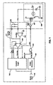
- FIG. 1 is a schematic illustration of one embodiment of the present invention
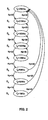
- FIG. 2 illustrates a state diagram of the control logic block of FIG. 1
- FIG. 3 is a comparison of a conventional pulse width modulation power output controller and a power output controller of the present invention as described in the embodiment of FIG. 1;
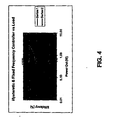
- FIG. 4 is a rspresentation of FIG. 3 with the scale of the x-axis shown as logarithmic;
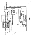
- FIG. 5 is a block diagram showing additional detail of the control logic block of FIG. 1;
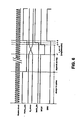
- FIG. 6 is a timing diagram of the control logic block of FIG. 5.
- an ultra-efficient switch mode controller topology uses variable, load dependent bandwidth adjustment to achieve ultra-low idle power objectives in battery operated systems, such as network powered cable communication services equipment and SLICs.
- battery operated systems such as network powered cable communication services equipment and SLICs.
- PWM pulse width modulated, or PWM
- FIGs. 1 and 5 illustrate the basic block diagram of the hysteretic controller of one embodiment of the present invention.
- This embodiment uses an inverted boost topology, as might be requited in a cable telephony application where apositive supply voltage, such as +12V, is converted to a negative battery supply, such as-48V.
- the power controller of one embodiment of the present invention includes a pulse generator 101 and a control logic block 102, both of which have a master clock 110 as an input.
- the pulse generator 101 outputs pulses that charge a capacitor 109 of an output stage 108 through an AND gate 103 and a level shifter 107.
- a sensing circuit 111 that includes an op amp 105 and a comparator 104 is used to sense a charging state of the capacitor 109.
- a fixed pulse width (for example, 2 ⁇ sec) variable frequency method is used.
- the control logic 102 uses an output of the sensing circuit Q_comp to count a number of output pulses (N P ) that occurred in a sliding time window that would allow, for example, 32 contiguous pulses at the particular switching frequency f i .
- the output voltage V OUT is preferably pre-filtered by the capacitor 125 to band limit the noise that the comparator 104 sees to avoid erroneous operation.
- the op amp 105 is used to generate a scaled down voltage proportional to the voltage V OUT on the capacitor 109. The scaled down voltage is fed into the inverting (-) input of the comparator 104.
- the programmable voltage reference V REF is provided by the control block 102 that allows the output voltage V OUT to vary depending on the desired state, for example -24V for telephony off-hook slates, -48V for on-hook states and-75V for ringing states.
- the reference voltage V REF which is outputted by the control logic 102, is fed into the non-inverting (+) input of the comparator 104. If the comparator 104 decides the magnitude of the output needs to increase, it will signal the control logic block 102 accordingly.
- the output Q_comp of the comparator 104 and the master clock 110 are inputted into the control logic 102, as further discussed below with reference to FIG. 5.
- FIG. 5. further illustrates the relationship between elements of the control block 102 and the pulse generator 101.
- the Q_comp signal from the comparator 104 is inputted into a DQ flip-flop 112 (a latch pulse).
- the master clock 110 (8.192 MHz in the preferred embodiment), is inputted into the pulse generator 101 and the clock input of the DQ flip-flop 112 as sys_clk.
- the pulse generator 101 outputs the Pulse_gen signal to the AND gate 103.
- the DQ flip-flop 112 outputs the latch_pls signal to the AND gate 103 as well.
- the Pulse_gen and latch_pls signals are ANDed by the AND gate 103, outputting the driver (DRV) signal.
- the DRV signal is inputted into the level shifter 107, as well as into a state machine/pulse counter 119 of the control block 102.
- the state machine/pulse counter 119 includes a 32 bit delay line 114, which uses the DRY signal and the Pulse_gen signal outputted by the pulse generator 101 as inputs. In the case of a window of pulses corresponding to 32 cycles of the Pulse_gen signal, the delay line 114 is essentially used to count how many times during the window the driver 103 was on.
- the 32 bit delay line 114 which is clocked by the Pulse_gen signal, outputs its output into a summer 117, The summer 117 therefore outputs the number of pulses N p outputted by the driver 103 during a paticular time window.
- the Pulse_gen signal also is inputted into a divide by 32 block 116.
- the summer 117 and the divide by 32 block 116 output their signals into a latch 118.
- the output of the latch 118 and the divide by 32 block 116 go into a state machine 115, which operates once every 32 cycles. The operation is described in additional detail below with reference to FIG. 2.
- the state machine 115 outputs a Freq signal (indicating at what frequency the pulse generator 101 should run) to the pulse generator 101 and to a latch generator 113.
- the pulse generator 101 also outputs a count_9B signal to the latch generator 113, and the latch generator 113 outputs an SCLK signal to the comparator 104, to enable the comparator 104.
- FIG. 6 illustrates a timing diagram of the control logic block 102 and the pulse generator 101 that are illustrated in FIGs. 1 and 5.
- the pulse generator 101 i.e., the Pulse_gen signal
- the comparator 104 outputs the Q_comp signal when the SCLK output of the latch generator 113 goes low. After the SCLK signal returns to high, the latch_pls signal goes high, and the output DRV of the AND gate 103 goes high, charging the capacitor 109.
- the capacitor 109 discharges rapidly, requiring a large number of pulses N P in a given time window to recharge.
- the pulse generator 101 only needs to output pulses at a rate of 16 KHz. If the control logic block 102 senses that in a given time window, the number of pulses N P required to charge the capacitor 109 is greater than a certain threshold (for example, 30 out of a maximum of 32), the frequency f i at which the pulse generator 101 charges the output stage will shift to 256 KHz (i.e., state S g ).
- control logic block 102 is in state S 2 or S 3 , which correspond to the pulse generator 101 frequencies of 32 KHz and 64 KHz, respectively.
- the frequencies f i are typically chosen to avoid a multiple or a submultiple of a frequency where there is some particular noise concern, so as to minimize interference with system operation.
- the operation of the state machine represented by the control logic block 102 may be thought of as follows; a number of possible states S 1 through S N exists in the state machine.
- the states may be thought of as M lower states S 1 through S M and N-M higher states, i.e., S M+1 though S N .
- For each state i there is a corresponding frequency f i (f 1 though f N ).
- For each state i there is a number of pulses N A1 which represent a threshold that triggers a shift to a higher state i+1.
- the digital controller includes a counter that monitors how many pulses have been output in the last N T (32 in one embodiment) Pulse_gen periods, continually updated on a sliding pulse-by-pulse scale.
- frequencies f i shown in the state diagram of FIG. 2 are believed to be optimum for the particular telephony (SLIC) application described above, it will be readily appreciated by one of ordinary skill in the art that these frequencies f i may be selected in accordance with a particular application, operating conditions and load ranges, and may vary on a case by case basis. It will also be appreciated that the number of states S 1 is not limited to that shown in FIG 2.
- components to the left of the dotted line in FIG. 1 represent circuitry that can be readily integrated in a low voltage CMOS process.
- the digital feedback loop provides control of the power converter over a wide range of switching frequencies as opposed to an analog feedback and control loop with fixed frequency operation. Moving the switching frequency to very low frequencies (constant on-time pulse width) provides very efficient power conversion at virtually no load, since the majority of losses are due to switching losses at low power. With multiple switching frequencies available, efficiency can be optimized for all load conditions, from no load to full load.
- a master clock 110 of 12.288Mhz may be used, with only six states, S 1 through S 6 , The states S 1 - S 6 correspond to frequencies of
- This embodiment could have greater performance depending on the overal system requirements.
- the pulse generator 101 may be constructed in any number of ways, as long as it generates the pulses that drive the circuit that provides current to the capacitor 109.
- it may be a separate generator, or implemented as part of the same IC as the control block 102.
- FIGs. 3 and 4 show the improvement in efficiency resulting from the use of the present invention. Both figures represent the same data, but FIG. 4 has a logarithmic scale on the x-axis, which allows abetter illustration of the efficiency at lower loads (e.g., the idle state),
- the lower curve in FIGs. 3 and 4 represents the related art efficiency, while the upper curve shows the efficiencies achieved with the power output controller of the present invention.
- This topology and control method can reduce system costs by easily allowing integration of the controller and elimination of variable compensation components required for different applications.
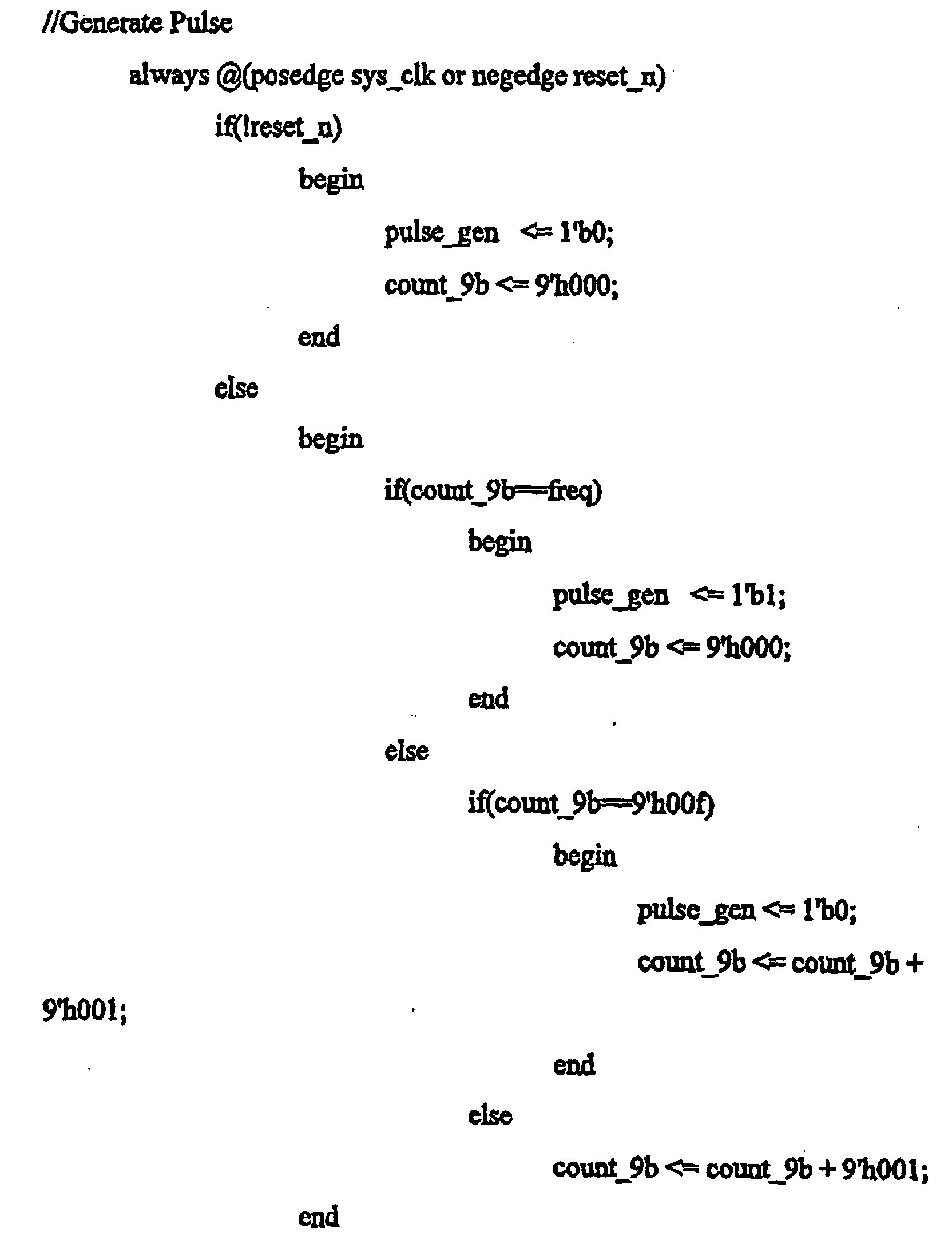
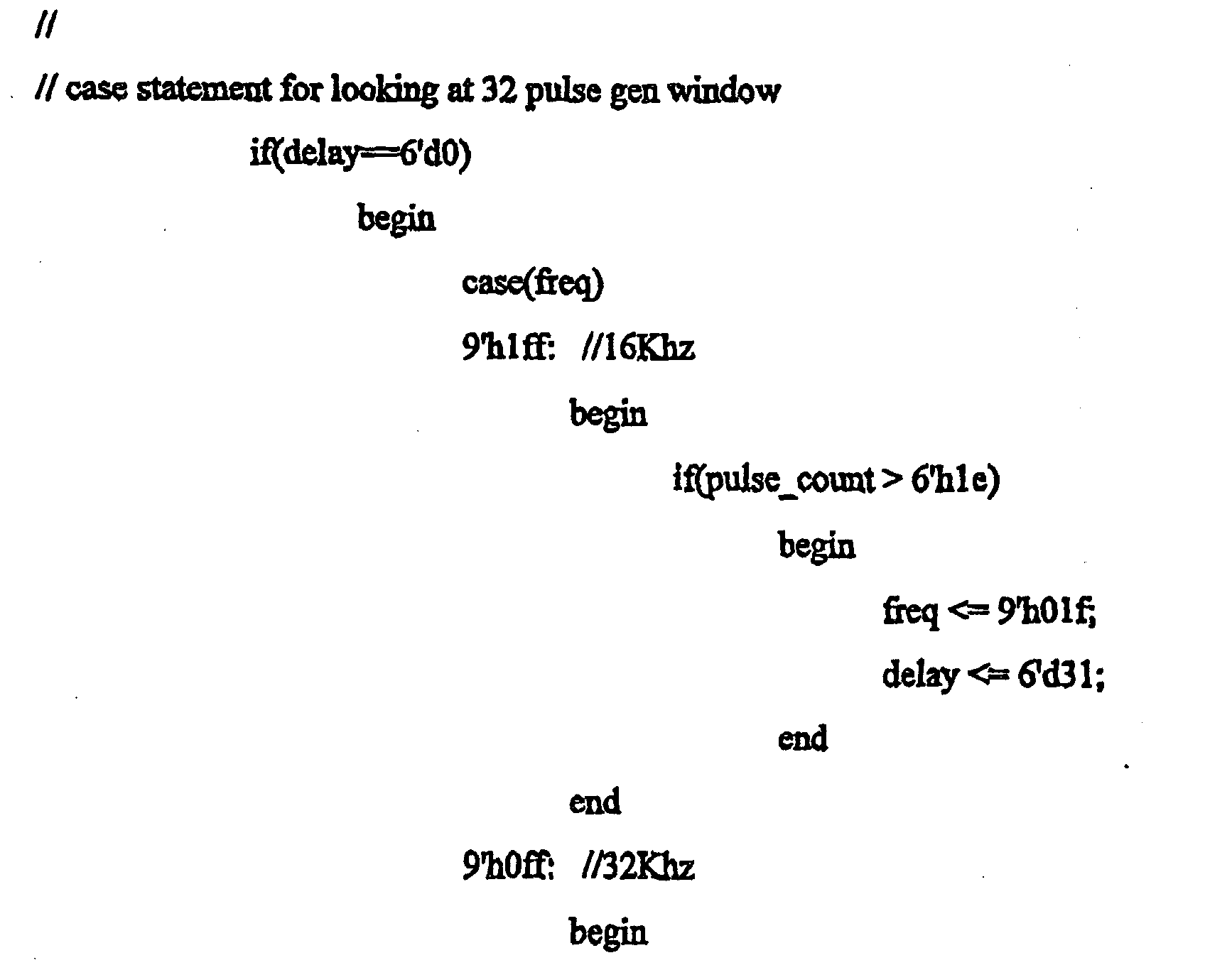
- the verilog code below illustrates one particular embodiment of the present invention, such as that shown in FIGs. 1 and 5. It will be understood that this embodiment is merely illustrative, and that the invention is not limited to this particular implementation.
- Pulse counter This circuit counts the number of pulses that occurs on the signal, driver during a period of 32 occurences of // pulse_gen .
- the 32 bit delay line is clockedkby the rising edge of pulse_gen . // This circuit controls the value of freq by looking at the accumulated pulse_count every 32 occurences of // pulse_gen .
- freq goes to the next lower freq state
- freq goes to the next higher freq state. Note that at 16,32 and 64 khz, if //the high theshold is crossed then the next state is the higher value of freq ,256khz, This allows the circuit to //quickly react to a high power requirement.
Landscapes
- Engineering & Computer Science (AREA)
- Power Engineering (AREA)
- Dc-Dc Converters (AREA)
- Programmable Controllers (AREA)
Abstract
Description

//make latchen_2 low for 5 cycles before rising edge of pulse


// This circuit counts the number of pulses that occurs on the signal, driver during a period of 32 occurences of //pulse_gen. The 32 bit delay line is clockedkby the rising edge of pulse_gen.




Claims (41)
- A power output controller comprising:an output stage;a sensing circuit for providing an output representative of an output voltage of the output stage; anda digital controller that controls output pulses that charge the output stage with a frequency that is dependent on the output of the sensing circuit.
- The power output controller of claim 1, wherein the output stage includes a capacitor being charged by the output pulses.
- The power output controller of claim 1, wherein the sensing circuit scales the output voltage prior to inputting the output voltage into a comparator.
- The power output controller of claim 1, wherein the sensing circuit includes an op amp for scaling the output voltage prior to inputting the output voltage into a comparator.
- The power output controller of claim 1, further including a pulse generator for generating the output pulses, the pulse generator being controlled by the digital controller.
- The power output controller of claim 1, wherein the digital controller lncludes a logic circuit having N states S1 through SN corresponding to N pulse frequencies fi (i=1 through N) and that controls output to the output stage, the pulse frequencies fi monotonically increasing.
- The power output controller of claim 6, wherein the N states include M states S1 through SM with lower frequencies f1 through fM and states SM+1 through SN with higher frequencies fM+1 through fN,
wherein the logic circuit switches to state SN from any of states S1 through SM when a number of pulses needed to charge the output stage exceeds a threshold number NAi for each state S1 through SN,
wherein the logic circuit switches to a next higher state from any of states SM+1 through SN-1 when the number of pulses needed to charge the output stage exceeds NAi for each corresponding state SM+1 through SN-1, and
wherein the logic circuit switches to a next lower state when the number of pulses needed to charge the output stage is less than a threshold number NBi for each state S2 through SN. - The power controller of claim 7, wherein NAi> NBi for each state.
- The power controller of claim 6, wherein the frequencies fi are programmable.
- A power controller comprising:wherein the N states include states S1 through SM with lower frequencies f1 through fM and states SM+1 through SN with higher frequencies fM+1 through fN, fN, andan output stage;a sensing circuit for providing an output corresponding to a voltage of the output stage;a pulse generator that charges the output stage; anda multi-state digital logic circuit having N states S, through SN corresponding to N pulse frequencies fi (i=1 through N) and that controls the pulse generator, the pulse frequencies fi monotonically increasing.
wherein the logic circuit switches to state SN from any of states S1 through SM when a number of pulses needed to charge the output stage exceeds a threshold number NAi for each state S1 through SM. - The power controller of claim 10, wherein the multi-state digital logic circuit switches to a next higher state from any of states SM+1 through SN-1 when the number of pulses needed to charge the output stage exceeds NA1 for each state SM+1 through SN-1.
- The power controller of claim 10, wherein the multi-state digital logic circuit switches to a next lower state when the number of pulses needed to charge the output stage is less than a threshold number NBI for each state S2 through SN.
- The power controller of claim 12, wherein NAi > NBi for each state.
- The power controller of claim 10, wherein the frequencies f1 are programmable.
- The power output controller of claim 10, wherein the sensing circuit scales the output voltage prior to inputting the output voltage into a comparator.
- The power output controller of claim 15, wherein the sensing circuit includes an op amp for scaling the output voltage prior to inputting the output voltage into the comparator.
- The power controller of claim 10, wherein the sensing circuit includes a comparator that compares the voltage of the output stage with a reference voltage.
- The power controller of claim 17, wherein the reference voltage is outputted by the multi-state digital logic circuit.
- The power controller of claim 10, wherein the output stage includes a capacitor being charged by the output pulses.
- A power controller comprising:wherein the N states include states S1 through SM with lower frequencies f1 through fM and states SM+1 through SN with higher frequencies fM+1 through fN,a sensing circuit that provides an output corresponding to a voltage of an output stage;a pulse generator that charges the output stage; anda digital logic circuit having N states S1 through SN corresponding to N pulse frequencies fi (i=1 thmugh N) and that controls the pulse generator based on the output of the sensing circuit, the pulse frequencies f1 monotonically increasing,
wherein the logic circuit switches to state SN from any of states S1 through SM when a number of pulses needed to charge the output stage exceeds a threshold number NA1 for each state S, through SM,
wherein the logic circuit switches to a next higher state from any of states SM+1 through SN-1 when a number of pulses needed to charge the output stage exceeds NA for each state SM+1 through SN-1, and
wherein the logic circuit switches to a next lower state when the number of pulses needed to charge the output stage is less than a threshold number NBi for each state S2 through SN. - The power controller of claim 20, wherein NAi>NBi for each state,
- The power controller of claim 20, wherein the sensing circuit includes a comparator that compares the voltage of the output stage with a reference voltage.
- The power output controller of claim 22, wherein the sensing circuit scales the output voltage prior to inputting the output voltage into the comparator.
- The power controller of claim 22, wherein the sensing circuit includes an op amp for scaling the output voltage before inputting the output voltage into the comparator.
- The power controller of claim 20, wherein the frequencies fi are programmable.
- The power controller of claim 20, wherein the output stage includes a capacitor being charged by the output pulses.
- A power output conteoller comprising:a sensing circuit that senses an output voltage of an output stage;a frequency modulated pulse generator that charges the output stage; anda multi-state digital controller that controls a frequency of pulses generated by the pulse generator based on information from the sensing circuit.
- The power controller of claim 27, wherein the sensing circuit includes a comparator that compares the output voltage with a reference voltage.
- The power output controller of claim 28, wherein the sensing circuit scales the output voltage prior to inputting the output voltage into a comparator.
- The power controller of claim 28, wherein the sensing circuit includes an op amp for scaling the output voltage before inputting the output voltage into the comparator.
- The power output controller of claim 27, wherein the output stage includes a capacitor being charged by the output pulses.
- The power output controller of claim 27, wherein the multi-state controller includes a logic circuit having N states S1 through SN corresponding to N pulse frequencies fi (i=1 throughN) and that controls output to the output stage, the pulse frequencies fi monotonically increasing.
- The power output controller of claim 32, wherein the N states include M states S1 through SM with lower frequencies f1 through fM and states SM+1 through SN with higher frequencies fM+1 through fN,
wherein the logic circuit switches to state SN from any of states S1 through SM when a number of pulses needed to charge the output stage exceeds a threshold number NAi for each corresponding state S1 through SM,
wherein the logic circuit switches to a next higher state from any of states SM+1 through SN-1 when a number of pulses needed to charge the output stage exceeds NAi for each state SM+1 through SN-1, and
wherein the logic circuit switches to a next lower state when the number of pulses needed to charge the output stage is less than a threshold number NBi for each state S2 through SN. - The power controller of claim 33, wherein NAi>NBi for each state.
- The power controller of claim 32, wherein the frequencies f1 are programmable.
- A method of controlling power output comprising the steps of:wherein the N states include M states S, through SM with lower frequencies fi through fM and states SM+1 through SN with higher frequencies fM+1 through fN, andsensing a voltage of an output stage;diving a pulse generator to charge the output stage; andcontrolling the pulse generator by using a multi-state digital logic circuit having N states S1 through SN corresponding to N pulse frequencies fi (i=1 through N), the pulse frequencies fi monotonically increasing,
wherein the digital logic circuit switches to state SN from any of states S1 through SM when a number of pulses needed to charge the output stage exceeds a threshold number NAi for each state S1 through SM. - The method of claim 36, wherein the digital logic circuit switches to a next higher state from any of states SM+1 through SN-1 when the number of pulses needed to charge the output stage exceeds NAi for each state SM+1 through SN-1,
- The method of claim 37, wherein the digital logic circuit switches to a next lower state when the number of pulses needed to charge the output stage is less than a threshold number NBi for each state S2 through SN.
- The method of claim 38, wherein NAi > NBi for each state.
- The method of claim 36, wherein the frequencies fi are programmable.
- A power output controller comprising:an output stage;a sensing circuit for providing an output representative of an output voltage of the output stage; anda controller that controls output pulses that charge the output stage with a frequency selected from a plurality of discrete frequencies and dependent on the output of the sensing circuit.
Applications Claiming Priority (4)
| Application Number | Priority Date | Filing Date | Title |
|---|---|---|---|
| US35089602P | 2002-01-25 | 2002-01-25 | |
| US350896P | 2002-01-25 | ||
| US10/244,407 US6853173B2 (en) | 2002-01-25 | 2002-09-17 | Programmable dual mode hysteretic power output controller |
| US244407 | 2002-09-17 |
Publications (3)
| Publication Number | Publication Date |
|---|---|
| EP1331720A2 true EP1331720A2 (en) | 2003-07-30 |
| EP1331720A3 EP1331720A3 (en) | 2005-12-14 |
| EP1331720B1 EP1331720B1 (en) | 2016-04-13 |
Family
ID=26936516
Family Applications (1)
| Application Number | Title | Priority Date | Filing Date |
|---|---|---|---|
| EP03001664.6A Expired - Lifetime EP1331720B1 (en) | 2002-01-25 | 2003-01-24 | Programmable dual mode hysteretic power output controller |
Country Status (2)
| Country | Link |
|---|---|
| US (1) | US6853173B2 (en) |
| EP (1) | EP1331720B1 (en) |
Families Citing this family (18)
| Publication number | Priority date | Publication date | Assignee | Title |
|---|---|---|---|---|
| US7570036B2 (en) * | 2004-09-10 | 2009-08-04 | Primarion Corporation | Multi-threshold multi-gain active transient response circuit and method for digital multiphase pulse width modulated regulators |
| US7521913B2 (en) * | 2004-09-10 | 2009-04-21 | Primarion Corporation | Active transient response circuits, system and method for digital multiphase pulse width modulated regulators |
| US6977492B2 (en) * | 2002-07-10 | 2005-12-20 | Marvell World Trade Ltd. | Output regulator |
| US6801028B2 (en) * | 2002-11-14 | 2004-10-05 | Fyre Storm, Inc. | Phase locked looped based digital pulse converter |
| US7439715B2 (en) * | 2006-05-22 | 2008-10-21 | Hamilton Sundstrand Corporation | Dual source power generating system |
| WO2009140404A2 (en) * | 2008-05-13 | 2009-11-19 | Igo , Inc. | Circuit and method for ultra-low idle power |
| US7779278B2 (en) * | 2008-05-29 | 2010-08-17 | Igo, Inc. | Primary side control circuit and method for ultra-low idle power operation |
| US7770039B2 (en) * | 2008-05-29 | 2010-08-03 | iGo, Inc | Primary side control circuit and method for ultra-low idle power operation |
| US7800252B2 (en) * | 2008-06-27 | 2010-09-21 | Igo, Inc. | Load condition controlled wall plate outlet system |
| US7795760B2 (en) * | 2008-07-25 | 2010-09-14 | Igo, Inc. | Load condition controlled power module |
| US7795759B2 (en) * | 2008-06-27 | 2010-09-14 | iGo, Inc | Load condition controlled power strip |
| US8207635B2 (en) * | 2009-02-20 | 2012-06-26 | Redwood Systems, Inc. | Digital switch communication |
| US8248230B2 (en) * | 2009-02-20 | 2012-08-21 | Redwood Systems, Inc. | Smart power device |
| US8427300B2 (en) | 2009-02-20 | 2013-04-23 | Redwood Systems, Inc. | Transmission of power and data with frequency modulation |
| US8058750B2 (en) * | 2009-05-14 | 2011-11-15 | Redwood Systems, Inc. | Discharge cycle communication |
| US8232791B2 (en) * | 2009-10-05 | 2012-07-31 | World Properties, Inc. | Soft starting driver for piezoelectric device |
| CN103795252B (en) * | 2012-10-31 | 2016-02-24 | 中兴通讯股份有限公司 | A kind of control method of series resonant converter |
| US20240235399A1 (en) * | 2023-01-05 | 2024-07-11 | Atmosic Technologies, Inc. | Power switching regulator for switching frequency avoidance |
Citations (1)
| Publication number | Priority date | Publication date | Assignee | Title |
|---|---|---|---|---|
| US5945820A (en) | 1997-02-06 | 1999-08-31 | The Board Of Trustees Of The Leland Stanford Junior University | DC-DC switching regulator with switching rate control |
Family Cites Families (12)
| Publication number | Priority date | Publication date | Assignee | Title |
|---|---|---|---|---|
| US588613A (en) * | 1897-08-24 | E morris petefts c | ||
| US3908163A (en) * | 1974-11-01 | 1975-09-23 | Allis Chalmers | Bandwidth limit circuit for step voltage regulator |
| US4066977A (en) * | 1976-03-30 | 1978-01-03 | E-Systems, Inc. | Digitized AGC amplifier with gain hysteresis circuit |
| US4531524A (en) * | 1982-12-27 | 1985-07-30 | Rdm International, Inc. | Circuit apparatus and method for electrothermal treatment of cancer eye |
| JP3727064B2 (en) * | 1994-06-03 | 2005-12-14 | コーニンクレッカ フィリップス エレクトロニクス エヌ ヴィ | Improved efficiency power supply and transmitter comprising such a power supply |
| EP0859454B1 (en) * | 1997-02-17 | 2002-10-02 | Asulab S.A. | Switch mode booster of a photovoltaic source voltage, especially for a timepiece |
| JP2985124B2 (en) * | 1997-06-12 | 1999-11-29 | 株式会社日立製作所 | Liquid crystal display |
| US6005377A (en) * | 1997-09-17 | 1999-12-21 | Lucent Technologies Inc. | Programmable digital controller for switch mode power conversion and power supply employing the same |
| US6198261B1 (en) * | 1998-10-30 | 2001-03-06 | Volterra Semiconductor Corporation | Method and apparatus for control of a power transistor in a digital voltage regulator |
| US6268716B1 (en) * | 1998-10-30 | 2001-07-31 | Volterra Semiconductor Corporation | Digital voltage regulator using current control |
| TW428363B (en) * | 1999-01-06 | 2001-04-01 | Faraday Tech Corp | Digital programmable DC voltage-drop converter |
| US6275018B1 (en) * | 2000-06-02 | 2001-08-14 | Iwatt | Switching power converter with gated oscillator controller |
-
2002
- 2002-09-17 US US10/244,407 patent/US6853173B2/en not_active Expired - Lifetime
-
2003
- 2003-01-24 EP EP03001664.6A patent/EP1331720B1/en not_active Expired - Lifetime
Patent Citations (1)
| Publication number | Priority date | Publication date | Assignee | Title |
|---|---|---|---|---|
| US5945820A (en) | 1997-02-06 | 1999-08-31 | The Board Of Trustees Of The Leland Stanford Junior University | DC-DC switching regulator with switching rate control |
Also Published As
| Publication number | Publication date |
|---|---|
| EP1331720B1 (en) | 2016-04-13 |
| EP1331720A3 (en) | 2005-12-14 |
| US20030141858A1 (en) | 2003-07-31 |
| US6853173B2 (en) | 2005-02-08 |
Similar Documents
| Publication | Publication Date | Title |
|---|---|---|
| EP1331720B1 (en) | Programmable dual mode hysteretic power output controller | |
| US5677619A (en) | Method and apparatus for multiple output regulation in a step-down switching regulator | |
| US7541795B1 (en) | Apparatus and method for start-up and over-current protection for a regulator | |
| US9391514B2 (en) | Device for controlling a switching mode power supply | |
| US7501805B2 (en) | Circuit and method for soft start from a residual voltage | |
| US9093901B2 (en) | Switching converter and method for controlling a switching converter | |
| CN115514228B (en) | Switching converter and its control circuit | |
| KR100927649B1 (en) | DC voltage converter | |
| US8269570B2 (en) | Systems and methods of ripple reduction in a DC/DC converter | |
| EP1078444A1 (en) | Pwm controller for use with open loop dc to ac converter | |
| US9667144B2 (en) | DC-DC converter with reverse current detecting circuit | |
| US7026795B2 (en) | Method for pulse modulation control of switching regulators | |
| KR102549239B1 (en) | Buck-boost converter using delta-sigma mudulator | |
| KR20050119213A (en) | Step-up/down dc-dc converter | |
| JP2004173421A (en) | DC / DC converter | |
| KR100576373B1 (en) | Digital DC-DC Converters Using Digital Modulation Techniques | |
| US20050237037A1 (en) | Switching power supply controller system and method | |
| US6275014B1 (en) | Switching regulator circuit capable of eliminating power supply recharging operation by reverse coil current | |
| CN105612683A (en) | Voltage regulator with charge pump for generating second voltage source | |
| US20090243578A1 (en) | Power Supply with Digital Control Loop | |
| CN110868067A (en) | Power converter and method for improving efficiency of power converter | |
| US20090243572A1 (en) | Power Supply with Digital Control Loop | |
| KR20210015457A (en) | Boost dc-dc converter using dsm, duty ratio controller for the boost dc-dc converter, and a method for configuring the duty ratio controller | |
| EP0998048B1 (en) | A method and device for controlling the power consumption of a mobile radio device | |
| EP0960470A1 (en) | Circuit and method for generating a voltage |
Legal Events
| Date | Code | Title | Description |
|---|---|---|---|
| PUAI | Public reference made under article 153(3) epc to a published international application that has entered the european phase |
Free format text: ORIGINAL CODE: 0009012 |
|
| AK | Designated contracting states |
Designated state(s): AT BE BG CH CY CZ DE DK EE ES FI FR GB GR HU IE IT LI LU MC NL PT SE SI SK TR |
|
| AX | Request for extension of the european patent |
Extension state: AL LT LV MK RO |
|
| PUAL | Search report despatched |
Free format text: ORIGINAL CODE: 0009013 |
|
| AK | Designated contracting states |
Kind code of ref document: A3 Designated state(s): AT BE BG CH CY CZ DE DK EE ES FI FR GB GR HU IE IT LI LU MC NL PT SE SI SK TR |
|
| AX | Request for extension of the european patent |
Extension state: AL LT LV MK RO |
|
| RIC1 | Information provided on ipc code assigned before grant |
Ipc: 7H 02M 3/10 A |
|
| 17P | Request for examination filed |
Effective date: 20060614 |
|
| AKX | Designation fees paid |
Designated state(s): DE FR GB |
|
| RAP1 | Party data changed (applicant data changed or rights of an application transferred) |
Owner name: BROADCOM CORPORATION |
|
| 17Q | First examination report despatched |
Effective date: 20100802 |
|
| GRAP | Despatch of communication of intention to grant a patent |
Free format text: ORIGINAL CODE: EPIDOSNIGR1 |
|
| INTG | Intention to grant announced |
Effective date: 20151111 |
|
| RIN1 | Information on inventor provided before grant (corrected) |
Inventor name: DUNN, WILLIAM ALVA Inventor name: WIER, CHARLES GARRISON Inventor name: CAINE, STEVEN LANCE |
|
| GRAS | Grant fee paid |
Free format text: ORIGINAL CODE: EPIDOSNIGR3 |
|
| GRAA | (expected) grant |
Free format text: ORIGINAL CODE: 0009210 |
|
| AK | Designated contracting states |
Kind code of ref document: B1 Designated state(s): DE FR GB |
|
| REG | Reference to a national code |
Ref country code: GB Ref legal event code: FG4D |
|
| REG | Reference to a national code |
Ref country code: DE Ref legal event code: R096 Ref document number: 60348785 Country of ref document: DE |
|
| REG | Reference to a national code |
Ref country code: DE Ref legal event code: R097 Ref document number: 60348785 Country of ref document: DE |
|
| PLBE | No opposition filed within time limit |
Free format text: ORIGINAL CODE: 0009261 |
|
| STAA | Information on the status of an ep patent application or granted ep patent |
Free format text: STATUS: NO OPPOSITION FILED WITHIN TIME LIMIT |
|
| 26N | No opposition filed |
Effective date: 20170116 |
|
| REG | Reference to a national code |
Ref country code: DE Ref legal event code: R119 Ref document number: 60348785 Country of ref document: DE |
|
| GBPC | Gb: european patent ceased through non-payment of renewal fee |
Effective date: 20170124 |
|
| REG | Reference to a national code |
Ref country code: FR Ref legal event code: ST Effective date: 20170929 |
|
| PG25 | Lapsed in a contracting state [announced via postgrant information from national office to epo] |
Ref country code: FR Free format text: LAPSE BECAUSE OF NON-PAYMENT OF DUE FEES Effective date: 20170131 |
|
| PG25 | Lapsed in a contracting state [announced via postgrant information from national office to epo] |
Ref country code: GB Free format text: LAPSE BECAUSE OF NON-PAYMENT OF DUE FEES Effective date: 20170124 Ref country code: DE Free format text: LAPSE BECAUSE OF NON-PAYMENT OF DUE FEES Effective date: 20170801 |