EP1331202A2 - Electronic device having an electrode made of metal on which carbon nanotubes are deposited - Google Patents
Electronic device having an electrode made of metal on which carbon nanotubes are deposited Download PDFInfo
- Publication number
- EP1331202A2 EP1331202A2 EP02257772A EP02257772A EP1331202A2 EP 1331202 A2 EP1331202 A2 EP 1331202A2 EP 02257772 A EP02257772 A EP 02257772A EP 02257772 A EP02257772 A EP 02257772A EP 1331202 A2 EP1331202 A2 EP 1331202A2
- Authority
- EP
- European Patent Office
- Prior art keywords
- electrode
- metal
- carbon
- electronic device
- oxygen
- Prior art date
- Legal status (The legal status is an assumption and is not a legal conclusion. Google has not performed a legal analysis and makes no representation as to the accuracy of the status listed.)
- Withdrawn
Links
Images



Classifications
-
- B—PERFORMING OPERATIONS; TRANSPORTING
- B82—NANOTECHNOLOGY
- B82Y—SPECIFIC USES OR APPLICATIONS OF NANOSTRUCTURES; MEASUREMENT OR ANALYSIS OF NANOSTRUCTURES; MANUFACTURE OR TREATMENT OF NANOSTRUCTURES
- B82Y10/00—Nanotechnology for information processing, storage or transmission, e.g. quantum computing or single electron logic
-
- B—PERFORMING OPERATIONS; TRANSPORTING
- B82—NANOTECHNOLOGY
- B82Y—SPECIFIC USES OR APPLICATIONS OF NANOSTRUCTURES; MEASUREMENT OR ANALYSIS OF NANOSTRUCTURES; MANUFACTURE OR TREATMENT OF NANOSTRUCTURES
- B82Y30/00—Nanotechnology for materials or surface science, e.g. nanocomposites
-
- B—PERFORMING OPERATIONS; TRANSPORTING
- B82—NANOTECHNOLOGY
- B82Y—SPECIFIC USES OR APPLICATIONS OF NANOSTRUCTURES; MEASUREMENT OR ANALYSIS OF NANOSTRUCTURES; MANUFACTURE OR TREATMENT OF NANOSTRUCTURES
- B82Y40/00—Manufacture or treatment of nanostructures
-
- C—CHEMISTRY; METALLURGY
- C01—INORGANIC CHEMISTRY
- C01B—NON-METALLIC ELEMENTS; COMPOUNDS THEREOF; METALLOIDS OR COMPOUNDS THEREOF NOT COVERED BY SUBCLASS C01C
- C01B32/00—Carbon; Compounds thereof
- C01B32/15—Nano-sized carbon materials
- C01B32/158—Carbon nanotubes
- C01B32/16—Preparation
- C01B32/162—Preparation characterised by catalysts
-
- H—ELECTRICITY
- H10—SEMICONDUCTOR DEVICES; ELECTRIC SOLID-STATE DEVICES NOT OTHERWISE PROVIDED FOR
- H10K—ORGANIC ELECTRIC SOLID-STATE DEVICES
- H10K10/00—Organic devices specially adapted for rectifying, amplifying, oscillating or switching; Organic capacitors or resistors having potential barriers
- H10K10/40—Organic transistors
- H10K10/46—Field-effect transistors, e.g. organic thin-film transistors [OTFT]
- H10K10/462—Insulated gate field-effect transistors [IGFETs]
-
- H—ELECTRICITY
- H10—SEMICONDUCTOR DEVICES; ELECTRIC SOLID-STATE DEVICES NOT OTHERWISE PROVIDED FOR
- H10K—ORGANIC ELECTRIC SOLID-STATE DEVICES
- H10K71/00—Manufacture or treatment specially adapted for the organic devices covered by this subclass
- H10K71/60—Forming conductive regions or layers, e.g. electrodes
-
- H—ELECTRICITY
- H10—SEMICONDUCTOR DEVICES; ELECTRIC SOLID-STATE DEVICES NOT OTHERWISE PROVIDED FOR
- H10K—ORGANIC ELECTRIC SOLID-STATE DEVICES
- H10K85/00—Organic materials used in the body or electrodes of devices covered by this subclass
- H10K85/20—Carbon compounds, e.g. carbon nanotubes or fullerenes
- H10K85/221—Carbon nanotubes
-
- H—ELECTRICITY
- H10—SEMICONDUCTOR DEVICES; ELECTRIC SOLID-STATE DEVICES NOT OTHERWISE PROVIDED FOR
- H10K—ORGANIC ELECTRIC SOLID-STATE DEVICES
- H10K10/00—Organic devices specially adapted for rectifying, amplifying, oscillating or switching; Organic capacitors or resistors having potential barriers
- H10K10/40—Organic transistors
- H10K10/46—Field-effect transistors, e.g. organic thin-film transistors [OTFT]
- H10K10/462—Insulated gate field-effect transistors [IGFETs]
- H10K10/466—Lateral bottom-gate IGFETs comprising only a single gate
Definitions
- the present invention relates to an electronic device, and more particularly, to an electronic device having an electrode which is proper to a case where carbon nanotubes are deposited on the electrode by chemical vapor deposition.
- carbon nanotubes are applied to a variety of types of electrode devices. For example, they can be applied to the fields of electron emitters, substances containing hydrogen, cathode materials for secondary cells, catalyzers, and sensors. In addition, more applications of carbon nanotubes are under development.
- a method using paste is inferior to a method using chemical vapor deposition in a characteristic such as selective deposition or alignment. Accordingly, it is predicted that the method using chemical vapor deposition will be widely used in manufacturing electronic devices.
- Representative chemical vapor deposition methods are a thermal chemical vapor deposition method and a plasma chemical vapor deposition method.
- the plasma chemical vapor deposition method is advantageous in synthesizing carbon nanotubes at a lower temperature than in a electric discharge method or a laser deposition method.
- the thermal chemical vapor deposition method is advantageous in synthesizing carbon nanotubes on a large area and synthesizing carbon nanotubes of high quality.
- methane (CH 4 ), acetylene (C 2 H 2 ), or carbon monoxide (CO) is used as a reactant gas for deposition of carbon nanotubes.
- This reactant gas is mixed with an etching gas such as hydrogen (H 2 ) or ammonia (NH 3 ).
- carbon nanotubes of good quality can be generated.
- carbon nanotubes can be deposited at a low temperature.
- Carbon monoxide allows the hydrogen impurity content of carbon nanotubes to be reduced so that carbon nanotubes of good quality can be deposited at a low temperature.
- carbon monoxide competes with oxygen atoms or radicals, which are generated during manufacturing of carbon nanotube, for chemical reaction with a metal or other carbon molecules, thereby oxidizing the metal or generating a product such as carbon dioxide.
- the surface of the metal oxidized by carbon monoxide is reduced in electrical conductivity, thereby disturbing the correct operation of electronic devices.
- an object of the present invention to provide an electronic device having an electrode, in which the electrical conductivity of the electrode is maintained constant and carbon nanotubes of good quality are formed on the electrode when the carbon nanotubes are deposited on the electrode using a chemical vapor deposition method.
- an electronic device having an electrode on which carbon nanotubes are deposited by a chemical vapor deposition method using a reactant gas containing carbon and oxygen.
- the electrode is made of a metal generating less reaction enthalpy when reacting with carbon than when reacting with oxygen.
- the metal is Ti or Mo.
- the metal reacts with carbon, forming a carbonized metal.
- the reactant gas is for example, carbon monoxide, carbon dioxide, methyl alcohol or ethyl alcohol.
- an electronic device having an electrode on which carbon nanotubes are deposited by a chemical vapor deposition method, the electron having a carbonized metal layer formed on a surface thereof.
- the carbonized metal layer prevents the electrode from being oxidized.
- the metal is Ti or Mo.
- the present invention uses a metal, which generates less reaction enthalpy when reacting with carbon than when reacting with oxygen, for an electrode, the metal of the electrode reacts with carbon prior to oxygen to form a carbonized metal layer on the surface of the electrode when a reactant gas containing carbon and oxygen is injected in a chemical vapor deposition apparatus. Due to the carbonized metal layer, oxygen cannot permeate into the electrode. Accordingly, the electrode is prevented from being oxidized, thereby maintaining the electrical conductivity of the electrode constant and increasing the yield of carbon nanotubes.
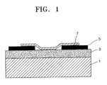
- FIG. 1 is a diagram of an electronic device having electrodes according to an embodiment of the present invention.
- an insulation layer 3 is deposited on a substrate 1
- two metal electrodes 5 in the form of foils are disposed to be separated from each other by a predetermined space at both sides on the surface of the insulation layer 3, and a carbon nanotube layer 7 connects the two metal electrodes 5.
- the structure is a most simple current-voltage (I-V) device if silicon is not doped with impurities and is a field-effect transistor (FET) if silicon is doped with P-type or N-type impurities.
- I-V current-voltage
- FET field-effect transistor
- the metal electrodes 5 of the electronic device are made of a metal such as titanium (Ti) or molybdenum (Mo).
- the metal generates less reaction enthalpy when reacting with carbon than when reacting with oxygen, so the metal reacts with carbon at higher speed than oxygen.
- FIG. 2 is a diagram for explaining a method of manufacturing an electronic device having electrodes according to the embodiment of the present invention using plasma chemical vapor deposition.
- a plasma chemical vapor deposition apparatus an upper electrode 14 and a lower electrode 12 are provided, and a substrate 11 on which a catalytic metal layer is formed is positioned on the lower electrode 12.
- a thermal resistance heater 13 positioned below the lower electrode 12 supplies heat to the substrate 11.
- a filament 15 is disposed between the upper electrode 14 and the lower electrode 12 to supply energy necessary for decomposing a reactant gas or synthesizing carbon nanotubes.
- a motor 19 rotates the lower electrode 12 on which the substrate 11 is positioned.
- a metal electrode 16 of an electron device to be manufactured is positioned on the surface of the catalytic metal layer on the substrate 11.
- the metal electrode 16 is made of a metal generating larger reaction enthalpy when reacting with carbon than when reacting with oxygen.
- the electronic device to be manufactured may have another layer having a different function, for example, an insulation layer, between the substrate 11 and the metal electrode 16.
- An RF power supply 17 is connected to the upper and lower electrodes 14 and 12 to supply electrical energy.
- a pipe for injecting a reactant gas is connected to the center of the upper electrode 14 so that a reactant gas such as carbon monoxide, methane, acetylene, or hydrogen is supplied to a reaction chamber 10.
- a glass, quartz, silicon, or alumina (Al 2 O 3 ) substrate may be used as the substrate 11.
- the metal electrode 16 of an electronic device may be made of a metal such as Ti, Mo, or iron (Fe) that reacts with carbon at higher speed than oxygen because it generates less reaction enthalpy when reacting with carbon than when reacting with oxygen.
- a metal such as Ti, Mo, or iron (Fe) that reacts with carbon at higher speed than oxygen because it generates less reaction enthalpy when reacting with carbon than when reacting with oxygen.
- Formula (1) is a chemical reaction formula illustrating the production of a carbonized metal when a metal reacts with carbon monoxide.
- Formula (2) illustrates a chemical reaction for producing an oxidized metal. 2 M + 2 CO ⁇ 2 MC + O 2 2 M + 2 CO ⁇ 2 MO + 2C
- the binding energy of TiO is 672.4 kJ/mol
- the binding energy of TiC is 423 kJ/mol
- a reaction enthalpy according to Formula (1) is -1307.1 kJ
- a reaction enthalpy according to Formula (2) is -808.2 kJ, so it can be inferred that the reaction according to Formula (1) is more dominant than the reaction according to Formula (2).
- the binding energy of MoO is 560.2 kJ/mol
- the binding energy of MoC is 481 kJ/mol
- a reaction enthalpy according to Formula (1) is -1191 kJ
- a reaction enthalpy according to Formula (2) is -1032 kJ, so it can be inferred that the reaction according to Formula (1) is more dominant than the reaction according to Formula (2).
- a carbonized metal such as carbon titanium, carbon molybdenum, or iron carbide is formed on the surface of a metal, thereby preventing the metal from contacting oxygen.
- a chemical reaction between carbon and metal and a chemical reaction between oxygen and metal are exothermic reactions, and a decrement in internal energy in the chemical reaction between carbon and metal is larger than a decrement in internal energy in the chemical reaction between oxygen and metal, so reaction enthalpy in the chemical reaction between carbon and metal is less than that in the chemical reaction between oxygen and metal.
- reaction enthalpy in the chemical reaction between carbon and metal is less than that in the chemical reaction between oxygen and metal.
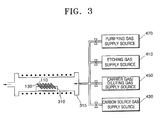
- An electronic device having an electrode made of a metal according to the embodiment of the present invention may be manufactured by a thermal chemical vapor deposition method.
- substrates 130 having electrodes 110 are arranged on a boat 310 of a thermal chemical vapor deposition apparatus to be separated from one another by a predetermined space in a line, and the boat 310 is loaded within a reaction furnace 315. Thereafter, the temperature of the reaction furnace 315 is raised to a process temperature, and an etching gas and a reactant gas are injected to the reaction furnace 315 to deposit carbon nanotubes on the electrodes 110.
- the electrode 16 or 110 is made of a metal such as Ti, Mo, or Fe that reacts with carbon better than with oxygen, so a carbonized metal layer is formed on the electrode 16 or 110. Accordingly, the electrode 16 or 110 is prevented from being oxidized during formation of carbon nanotubes. Since electrical conductivity is maintained constant, an electronic device can be easily manufactured. Therefore, an electronic device having good performance can be manufactured.
- FIG. 4 is a graph showing a change in an atom concentration (%) with respect to a chrome (Cr) electrode, which has been exposed to the conditions of carbon nanotube manufacturing using a mixed gas of carbon monoxide and hydrogen as a reactant gas, in the form of an Auger electron spectrum.
- chrome reacts with oxygen prior to carbon so as to form chrome oxide (CrO x )
- CrO x chrome oxide
- a Cr-atom concentration is small to a predetermined depth from the surface but increases as the depth is deeper into the inside of the chrome electrode.
- oxygen which is familiar with chrome is adsorbed to the surface of the chrome electrode much, so an O-atom concentration is high to a predetermined depth from the surface but decreases as the depth is deeper into the inside of the chrome electrode.
- Carbon hardly reacts with chrome, so a C-atom concentration is maintained nearly constant.
- FIG. 5A is a graph showing a change in an atom concentration with respect to an aluminum (Al) electrode, which has been exposed to the conditions of carbon nanotube manufacturing using a mixed gas of carbon monoxide and hydrogen as a reactant gas, in the form of an X-ray photoelectron spectrum.
- an Al-atom concentration increases while an O-atom concentration decreases as a depth from the surface of the aluminum electrode is deeper.
- Aluminum reacts with oxygen or hydrogen, thereby producing alumina (Al 2 O 3 ) or aluminum hydride (AIH x , for example, AlH 3 ).
- alumina Al 2 O 3
- AIH x aluminum hydride
- FIG. 5 As the depth from the surface of the aluminum electrode is deeper, more aluminum hydride is produced.
- aluminum hydride is more produced than alumina.
- aluminum hydride has a low melting point, so aluminum is inappropriate for the electrode.
- FIG. 6 is a graph showing a change in an atom concentration with respect to a molybdenum (Mo) electrode, which is included in an electron device according to the embodiment of the present invention and which has been exposed to the conditions of carbon nanotube manufacturing using a mixed gas of carbon monoxide and hydrogen as a reactant gas, in the form of an X-ray photoelectron spectrum.
- Mo molybdenum
- an electronic device in the case of using a reactant gas containing carbon and oxygen in forming carbon nanotubes, an electronic device has an electrode made of a metal that reacts with carbon at higher speed than oxygen because it generates less reaction enthalpy when reacting with carbon than when reacting with oxygen so that a carbonized metal layer is formed on the surface of the electrode to prevent oxidization. Accordingly, carbon nanotubes can be grown on the electronic device under a state in which the electrical conductivity of the electrode is maintained constant, thereby improving the performance of the electronic device.
- an electronic device has an electrode made of a metal which reacts with carbon better than with oxygen so that a carbonized metal layer is formed on the electrode so as to prevent oxidization of the electrode.
- the electrical conductivity of the electrode is maintained constant, thereby allowing carbon nanotubes to be formed by various methods and improving the entire performance of the electronic device.
Landscapes
- Engineering & Computer Science (AREA)
- Chemical & Material Sciences (AREA)
- Nanotechnology (AREA)
- Materials Engineering (AREA)
- Crystallography & Structural Chemistry (AREA)
- Physics & Mathematics (AREA)
- Manufacturing & Machinery (AREA)
- Condensed Matter Physics & Semiconductors (AREA)
- General Physics & Mathematics (AREA)
- Organic Chemistry (AREA)
- Composite Materials (AREA)
- Mathematical Physics (AREA)
- Theoretical Computer Science (AREA)
- Chemical Kinetics & Catalysis (AREA)
- Inorganic Chemistry (AREA)
- Carbon And Carbon Compounds (AREA)
- Electrodes Of Semiconductors (AREA)
- Electrochromic Elements, Electrophoresis, Or Variable Reflection Or Absorption Elements (AREA)
- Ceramic Capacitors (AREA)
- Cold Cathode And The Manufacture (AREA)
Abstract
Description
- The present invention relates to an electronic device, and more particularly, to an electronic device having an electrode which is proper to a case where carbon nanotubes are deposited on the electrode by chemical vapor deposition.
- Due to peculiar structural and electrical characteristics, carbon nanotubes are applied to a variety of types of electrode devices. For example, they can be applied to the fields of electron emitters, substances containing hydrogen, cathode materials for secondary cells, catalyzers, and sensors. In addition, more applications of carbon nanotubes are under development.
- In manufacturing electron devices using carbon nanotubes, a method using carbon nanotubes in the form of powder or paste or a method of directly depositing carbon nanotubes on a substrate using chemical vapor deposition is used.
- In a method of manufacturing electron devices using carbon nanotube powder or paste, laser ablation or arc discharge is performed on carbon nanotubes to obtain carbon nanotube powder, the carbon nanotube powder is mixed with conductive or nonconductive paste, and then printing is performed.
- A method using paste is inferior to a method using chemical vapor deposition in a characteristic such as selective deposition or alignment. Accordingly, it is predicted that the method using chemical vapor deposition will be widely used in manufacturing electronic devices.
- Representative chemical vapor deposition methods are a thermal chemical vapor deposition method and a plasma chemical vapor deposition method. The plasma chemical vapor deposition method is advantageous in synthesizing carbon nanotubes at a lower temperature than in a electric discharge method or a laser deposition method. The thermal chemical vapor deposition method is advantageous in synthesizing carbon nanotubes on a large area and synthesizing carbon nanotubes of high quality.
- In the above chemical vapor deposition methods, methane (CH4), acetylene (C2H2), or carbon monoxide (CO) is used as a reactant gas for deposition of carbon nanotubes. This reactant gas is mixed with an etching gas such as hydrogen (H2) or ammonia (NH3).
- When methane is used as a reactant gas in a case using high-energy plasma, carbon nanotubes of good quality can be generated. When acetylene is used as a reactant gas, carbon nanotubes can be deposited at a low temperature.
- Carbon monoxide allows the hydrogen impurity content of carbon nanotubes to be reduced so that carbon nanotubes of good quality can be deposited at a low temperature. However, carbon monoxide competes with oxygen atoms or radicals, which are generated during manufacturing of carbon nanotube, for chemical reaction with a metal or other carbon molecules, thereby oxidizing the metal or generating a product such as carbon dioxide. The surface of the metal oxidized by carbon monoxide is reduced in electrical conductivity, thereby disturbing the correct operation of electronic devices.
- In other words, when gas such as carbon monoxide, carbon dioxide (CO2), methyl alcohol (CH3OH), or ethyl alcohol (C2H5OH) containing oxygen is used as a reactant gas in a conventional chemical vapor deposition apparatus, the reactant gas reacts with a metal forming electrodes and oxidizes it, thereby decreasing electrical conductivity of the electrodes. Consequently, performance of electronic devices is decreased.
- To solve the above-described problems, it is an object of the present invention to provide an electronic device having an electrode, in which the electrical conductivity of the electrode is maintained constant and carbon nanotubes of good quality are formed on the electrode when the carbon nanotubes are deposited on the electrode using a chemical vapor deposition method.
- To achieve the above object of the present invention, in one aspect, there is provided an electronic device having an electrode on which carbon nanotubes are deposited by a chemical vapor deposition method using a reactant gas containing carbon and oxygen. The electrode is made of a metal generating less reaction enthalpy when reacting with carbon than when reacting with oxygen.
- Preferably, the metal is Ti or Mo.
- Preferably, the metal reacts with carbon, forming a carbonized metal.
- The reactant gas is for example, carbon monoxide, carbon dioxide, methyl alcohol or ethyl alcohol.
- In another aspect, there is provided an electronic device having an electrode on which carbon nanotubes are deposited by a chemical vapor deposition method, the electron having a carbonized metal layer formed on a surface thereof. The carbonized metal layer prevents the electrode from being oxidized.
- Preferably, the metal is Ti or Mo.
- Since the present invention uses a metal, which generates less reaction enthalpy when reacting with carbon than when reacting with oxygen, for an electrode, the metal of the electrode reacts with carbon prior to oxygen to form a carbonized metal layer on the surface of the electrode when a reactant gas containing carbon and oxygen is injected in a chemical vapor deposition apparatus. Due to the carbonized metal layer, oxygen cannot permeate into the electrode. Accordingly, the electrode is prevented from being oxidized, thereby maintaining the electrical conductivity of the electrode constant and increasing the yield of carbon nanotubes.
- The above object and advantages of the present invention will become more apparent by describing in detail a preferred embodiment thereof with reference to the attached drawings in which:
- FIG. 1 is a diagram of an electronic device having electrodes according to an embodiment of the present invention;
- FIG. 2 is a diagram for explaining a method of manufacturing an electronic device having electrodes according to the embodiment of the present invention using plasma chemical vapor deposition;
- FIG. 3 is a diagram for explaining a method of manufacturing an electronic device having electrodes according to the embodiment of the present invention using thermal chemical vapor deposition;
- FIG. 4 is a graph of changes in an atom concentration versus sputter time after a chrome electrode is exposed to carbon nanotube deposition conditions;
- FIG. 5A is a graph of changes in an atom concentration versus sputter time after an aluminum electrode is exposed to carbon nanotube deposition conditions;
- FIG. 5B is a graph of count/second (C/S) versus binding energy after an aluminum electrode is exposed to carbon nanotube deposition conditions; and
- FIG. 6 is a graph of changes in an atom concentration versus sputter time after a molybdenum electrode is exposed to carbon nanotube deposition conditions.
-
- Hereinafter, an electronic device having electrodes according to the embodiment of the present invention will be described in detail with reference to the attached drawings.
- FIG. 1 is a diagram of an electronic device having electrodes according to an embodiment of the present invention. Referring to FIG. 1, an
insulation layer 3 is deposited on a substrate 1, twometal electrodes 5 in the form of foils are disposed to be separated from each other by a predetermined space at both sides on the surface of theinsulation layer 3, and acarbon nanotube layer 7 connects the twometal electrodes 5. - The structure is a most simple current-voltage (I-V) device if silicon is not doped with impurities and is a field-effect transistor (FET) if silicon is doped with P-type or N-type impurities.
- The
metal electrodes 5 of the electronic device are made of a metal such as titanium (Ti) or molybdenum (Mo). The metal generates less reaction enthalpy when reacting with carbon than when reacting with oxygen, so the metal reacts with carbon at higher speed than oxygen. - FIG. 2 is a diagram for explaining a method of manufacturing an electronic device having electrodes according to the embodiment of the present invention using plasma chemical vapor deposition. Referring to FIG. 2, in a plasma chemical vapor deposition apparatus, an
upper electrode 14 and alower electrode 12 are provided, and asubstrate 11 on which a catalytic metal layer is formed is positioned on thelower electrode 12. Athermal resistance heater 13 positioned below thelower electrode 12 supplies heat to thesubstrate 11. Afilament 15 is disposed between theupper electrode 14 and thelower electrode 12 to supply energy necessary for decomposing a reactant gas or synthesizing carbon nanotubes. Amotor 19 rotates thelower electrode 12 on which thesubstrate 11 is positioned. - A
metal electrode 16 of an electron device to be manufactured is positioned on the surface of the catalytic metal layer on thesubstrate 11. Themetal electrode 16 is made of a metal generating larger reaction enthalpy when reacting with carbon than when reacting with oxygen. Here, the electronic device to be manufactured may have another layer having a different function, for example, an insulation layer, between thesubstrate 11 and themetal electrode 16. - An
RF power supply 17 is connected to the upper andlower electrodes upper electrode 14 so that a reactant gas such as carbon monoxide, methane, acetylene, or hydrogen is supplied to areaction chamber 10. - When RF power is supplied under a state in which a predetermined pressure is maintained at a temperature of no greater than about 660EC after an etching gas such as ammonia gas or hydrogen gas is injected into the
reaction chamber 10, the surface of themetal electrode 16 on thesubstrate 11 is etched by plasma generated from the etching gas, thereby forming catalytic corpuscles in the forms of fine grains on the surface of themetal electrode 16. Carbon nanotubes are synthesized to be vertically arranged on the catalytic corpuscles. - A glass, quartz, silicon, or alumina (Al2O3) substrate may be used as the
substrate 11. - The
metal electrode 16 of an electronic device may be made of a metal such as Ti, Mo, or iron (Fe) that reacts with carbon at higher speed than oxygen because it generates less reaction enthalpy when reacting with carbon than when reacting with oxygen. - Formula (1) is a chemical reaction formula illustrating the production of a carbonized metal when a metal reacts with carbon monoxide. Formula (2) illustrates a chemical reaction for producing an oxidized metal.
- In the case of Ti, the binding energy of TiO is 672.4 kJ/mol, the binding energy of TiC is 423 kJ/mol, a reaction enthalpy according to Formula (1) is -1307.1 kJ, and a reaction enthalpy according to Formula (2) is -808.2 kJ, so it can be inferred that the reaction according to Formula (1) is more dominant than the reaction according to Formula (2).
- In the case of Mo, the binding energy of MoO is 560.2 kJ/mol, the binding energy of MoC is 481 kJ/mol, a reaction enthalpy according to Formula (1) is -1191 kJ, and a reaction enthalpy according to Formula (2) is -1032 kJ, so it can be inferred that the reaction according to Formula (1) is more dominant than the reaction according to Formula (2).
- However, in the case of Cr, while the binding energy of CrO is 429.3 kJ/mol, the binding energy of CrC is much higher than 429.3 kJ/mol, so the reaction according to Formula (2) is more dominant than the reaction according to Formula (1).
- Accordingly, when gas such as carbon monoxide, carbon dioxide, methyl alcohol, or ethyl alcohol containing oxygen is used as a reaction gas, a carbonized metal such as carbon titanium, carbon molybdenum, or iron carbide is formed on the surface of a metal, thereby preventing the metal from contacting oxygen.
- Internal energy decreases, resulting in a negative reaction enthalpy when chemical reaction is of exothermic type, and increases, resulting in a positive reaction enthalpy when the chemical reaction is of endothermic type. In the present invention, a chemical reaction between carbon and metal and a chemical reaction between oxygen and metal are exothermic reactions, and a decrement in internal energy in the chemical reaction between carbon and metal is larger than a decrement in internal energy in the chemical reaction between oxygen and metal, so reaction enthalpy in the chemical reaction between carbon and metal is less than that in the chemical reaction between oxygen and metal. In other words, more heat is generated when a carbonized metal is produced by the reaction between carbon and metal than when an oxidized metal is produced by the reaction between oxygen and metal. Therefore, it can be inferred that a carbonized metal is safer than an oxidized metal.
- An electronic device having an electrode made of a metal according to the embodiment of the present invention may be manufactured by a thermal chemical vapor deposition method.
- Referring to FIG. 3,
substrates 130 havingelectrodes 110 are arranged on aboat 310 of a thermal chemical vapor deposition apparatus to be separated from one another by a predetermined space in a line, and theboat 310 is loaded within areaction furnace 315. Thereafter, the temperature of thereaction furnace 315 is raised to a process temperature, and an etching gas and a reactant gas are injected to thereaction furnace 315 to deposit carbon nanotubes on theelectrodes 110. - Descriptions of the
substrates 130, theelectrodes 110, and the reactant gas are the same as those in the plasma chemical vapor deposition method, and thus they will be omitted. - According to the present invention, when an electronic device such as a transistor or a field emitter display (FED) is manufactured by a thermal chemical vapor deposition method or a plasma chemical vapor deposition method, the
electrode electrode electrode - FIG. 4 is a graph showing a change in an atom concentration (%) with respect to a chrome (Cr) electrode, which has been exposed to the conditions of carbon nanotube manufacturing using a mixed gas of carbon monoxide and hydrogen as a reactant gas, in the form of an Auger electron spectrum.
- Referring to FIG. 4, as the sputter time elapses 1500 sec, a Cr-atom concentration increases while an oxygen (O)-atom concentration decreases. A carbon (C)-atom concentration is almost constant.
- Since chrome reacts with oxygen prior to carbon so as to form chrome oxide (CrOx), a Cr-atom concentration is small to a predetermined depth from the surface but increases as the depth is deeper into the inside of the chrome electrode. In contrast, oxygen which is familiar with chrome is adsorbed to the surface of the chrome electrode much, so an O-atom concentration is high to a predetermined depth from the surface but decreases as the depth is deeper into the inside of the chrome electrode. Carbon hardly reacts with chrome, so a C-atom concentration is maintained nearly constant.
- It can be seen from the graph that chrome is more familiar with oxygen than carbon, so it can be inferred that chrome is inappropriate for the electrode.
- FIG. 5A is a graph showing a change in an atom concentration with respect to an aluminum (Al) electrode, which has been exposed to the conditions of carbon nanotube manufacturing using a mixed gas of carbon monoxide and hydrogen as a reactant gas, in the form of an X-ray photoelectron spectrum.
- Referring to FIG. 5A, an Al-atom concentration increases while an O-atom concentration decreases as a depth from the surface of the aluminum electrode is deeper.
- Aluminum reacts with oxygen or hydrogen, thereby producing alumina (Al2O3) or aluminum hydride (AIHx, for example, AlH3). Referring to FIG. 5, as the depth from the surface of the aluminum electrode is deeper, more aluminum hydride is produced. In other words, it is inferred from the results only shown in FIG. 5A that aluminum mainly reacts with oxygen to produce alumina on the surface of the electrode, but it can be newly inferred from the graph shown in FIG. 5B that aluminum hydride is more produced than alumina. However, aluminum hydride has a low melting point, so aluminum is inappropriate for the electrode.
- FIG. 6 is a graph showing a change in an atom concentration with respect to a molybdenum (Mo) electrode, which is included in an electron device according to the embodiment of the present invention and which has been exposed to the conditions of carbon nanotube manufacturing using a mixed gas of carbon monoxide and hydrogen as a reactant gas, in the form of an X-ray photoelectron spectrum.
- As shown in FIG. 6, as an etching process proceeds, a C-atom concentration decreases while a Mo-atom concentration increases and an O-atom concentration is maintained nearly constant. This is because a molybdenum carbide layer is formed on only the surface of the electrode and a metal property is maintained inside the electrode. It can be inferred from this graph that molybdenum is appropriate for the electrode used in an electronic device according to the embodiment of the present invention.
- The following table shows changes in electrical conductivity of different metals. A unit is l/Ω cm.
Metal Cr Mo Ti Ni Al Before reaction 0.2 0.4 0.3 0.4 0.2 After reaction >10-6 1.2 1.0 15.7 0.6 - While the electrical conductivity of chrome greatly decreases after reaction in a chemical vapor deposition apparatus, the electrical conductivities of the other metals hardly change. It can be inferred from the above table that electrical energy can be constantly supplied when an electrode is made of one of the four metals except chrome. However, aluminum may sublimate in the form of aluminum hybrid, so it is not appropriate for an electrode.
- According to the embodiment of the present invention, in the case of using a reactant gas containing carbon and oxygen in forming carbon nanotubes, an electronic device has an electrode made of a metal that reacts with carbon at higher speed than oxygen because it generates less reaction enthalpy when reacting with carbon than when reacting with oxygen so that a carbonized metal layer is formed on the surface of the electrode to prevent oxidization. Accordingly, carbon nanotubes can be grown on the electronic device under a state in which the electrical conductivity of the electrode is maintained constant, thereby improving the performance of the electronic device.
- As described above, according to the present invention, an electronic device has an electrode made of a metal which reacts with carbon better than with oxygen so that a carbonized metal layer is formed on the electrode so as to prevent oxidization of the electrode. As a result, the electrical conductivity of the electrode is maintained constant, thereby allowing carbon nanotubes to be formed by various methods and improving the entire performance of the electronic device.
Claims (6)
- An electronic device having an electrode on which carbon nanotubes are deposited by a chemical vapor deposition method using a reactant gas containing carbon and oxygen, the electrode being made of a metal which generates less reaction enthalpy when reacting with carbon than when reacting with oxygen.
- The electronic device according to claim 1, wherein the metal is Ti or Mo.
- The electronic device according to claim 2, wherein the metal is one which reacts with carbon to form a carbonized metal.
- The electronic device according to claim 1, wherein the reactant gas is carbon monoxide, carbon dioxide, methyl alcohol or ethyl alcohol.
- An electronic device having an electrode on which carbon nanotubes are deposited by a chemical vapor deposition method, the electrode having a carbonized metal layer formed on a surface thereof, the carbonized metal layer preventing the electrode from being oxidized.
- The electronic device according to claim 5, wherein the metal is Ti or Mo.
Applications Claiming Priority (2)
| Application Number | Priority Date | Filing Date | Title |
|---|---|---|---|
| KR1020020003688A KR100837393B1 (en) | 2002-01-22 | 2002-01-22 | Electronic device having a metal having high affinity for carbon as an electrode |
| KR2002003688 | 2002-01-22 |
Publications (2)
| Publication Number | Publication Date |
|---|---|
| EP1331202A2 true EP1331202A2 (en) | 2003-07-30 |
| EP1331202A3 EP1331202A3 (en) | 2005-01-19 |
Family
ID=19718736
Family Applications (1)
| Application Number | Title | Priority Date | Filing Date |
|---|---|---|---|
| EP02257772A Withdrawn EP1331202A3 (en) | 2002-01-22 | 2002-11-08 | Electronic device having an electrode made of metal on which carbon nanotubes are deposited |
Country Status (5)
| Country | Link |
|---|---|
| US (2) | US20040214429A1 (en) |
| EP (1) | EP1331202A3 (en) |
| JP (1) | JP2003331711A (en) |
| KR (1) | KR100837393B1 (en) |
| CN (1) | CN1319114C (en) |
Cited By (7)
| Publication number | Priority date | Publication date | Assignee | Title |
|---|---|---|---|---|
| FR2860780A1 (en) * | 2003-10-13 | 2005-04-15 | Centre Nat Rech Scient | METHOD FOR SYNTHESIS OF NANOMETRIC FILAMENT STRUCTURES AND COMPONENTS FOR ELECTRONICS COMPRISING SUCH STRUCTURES |
| WO2005069412A1 (en) * | 2004-01-14 | 2005-07-28 | Kh Chemicals Co., Ltd. | Carbon nanotube or carbon nanofiber electrode comprising sulfur or metal nanoparticles as a binder and process for preparing the same |
| US7531267B2 (en) | 2003-06-02 | 2009-05-12 | Kh Chemicals Co., Ltd. | Process for preparing carbon nanotube electrode comprising sulfur or metal nanoparticles as a binder |
| CN1608980B (en) * | 2003-07-31 | 2011-08-03 | 株式会社半导体能源研究所 | Method for manufacturing ultrafine carbon fiber and field emission element |
| EP2259043A4 (en) * | 2008-02-27 | 2012-06-27 | Japan Science & Tech Agency | CARBON NANOTUBE SUPPORT AND METHOD FOR PRODUCING THE CARBON NANOTUBE SUPPORT |
| US9506194B2 (en) | 2012-09-04 | 2016-11-29 | Ocv Intellectual Capital, Llc | Dispersion of carbon enhanced reinforcement fibers in aqueous or non-aqueous media |
| CN110295296A (en) * | 2019-08-16 | 2019-10-01 | 深圳利都科技有限公司 | A kind of preparation method of molybdenum base carbon nano electronic encapsulating material |
Families Citing this family (21)
| Publication number | Priority date | Publication date | Assignee | Title |
|---|---|---|---|---|
| US8958917B2 (en) | 1998-12-17 | 2015-02-17 | Hach Company | Method and system for remote monitoring of fluid quality and treatment |
| US9056783B2 (en) | 1998-12-17 | 2015-06-16 | Hach Company | System for monitoring discharges into a waste water collection system |
| US7454295B2 (en) | 1998-12-17 | 2008-11-18 | The Watereye Corporation | Anti-terrorism water quality monitoring system |
| US8920619B2 (en) | 2003-03-19 | 2014-12-30 | Hach Company | Carbon nanotube sensor |
| JP4620401B2 (en) * | 2004-07-21 | 2011-01-26 | 三菱電機株式会社 | Semiconductor laser element |
| US7598516B2 (en) * | 2005-01-07 | 2009-10-06 | International Business Machines Corporation | Self-aligned process for nanotube/nanowire FETs |
| KR20070003467A (en) * | 2005-07-02 | 2007-01-05 | 삼성전자주식회사 | Surface light source device and liquid crystal display device including the same |
| EP2089418B1 (en) * | 2006-12-04 | 2016-11-09 | Ramot at Tel-Aviv University Ltd. | Formation of organic nanostructure array |
| DE102007006444B4 (en) * | 2007-02-05 | 2015-05-13 | Airbus Defence and Space GmbH | Micro-engine, in particular for use as attitude control engine, small engine and method for manufacturing a micro-engine |
| JP4875517B2 (en) * | 2007-03-05 | 2012-02-15 | シャープ株式会社 | Chemical substance sensing element, chemical substance sensing device, and method of manufacturing chemical substance sensing element |
| FR2922364B1 (en) * | 2007-10-12 | 2014-08-22 | Saint Gobain | PROCESS FOR PRODUCING A MOLYBDENE OXIDE ELECTRODE |
| KR101001477B1 (en) * | 2009-02-27 | 2010-12-14 | 아주대학교산학협력단 | Atmospheric Low Temperature Micro Plasma Injection Apparatus for Bio-Medical Applications |
| US8624396B2 (en) | 2012-06-14 | 2014-01-07 | Taiwan Semiconductor Manufacturing Company, Ltd. | Apparatus and method for low contact resistance carbon nanotube interconnect |
| US10418647B2 (en) | 2015-04-15 | 2019-09-17 | Lockheed Martin Energy, Llc | Mitigation of parasitic reactions within flow batteries |
| JP2018529189A (en) | 2015-08-19 | 2018-10-04 | ロッキード マーティン エナジー, エルエルシーLockheed Martin Energy, Llc | Solid reduction in flow battery |
| US10381674B2 (en) | 2016-04-07 | 2019-08-13 | Lockheed Martin Energy, Llc | High-throughput manufacturing processes for making electrochemical unit cells and electrochemical unit cells produced using the same |
| US10147957B2 (en) | 2016-04-07 | 2018-12-04 | Lockheed Martin Energy, Llc | Electrochemical cells having designed flow fields and methods for producing the same |
| US10109879B2 (en) | 2016-05-27 | 2018-10-23 | Lockheed Martin Energy, Llc | Flow batteries having an electrode with a density gradient and methods for production and use thereof |
| US10403911B2 (en) | 2016-10-07 | 2019-09-03 | Lockheed Martin Energy, Llc | Flow batteries having an interfacially bonded bipolar plate-electrode assembly and methods for production and use thereof |
| US10573899B2 (en) | 2016-10-18 | 2020-02-25 | Lockheed Martin Energy, Llc | Flow batteries having an electrode with differing hydrophilicity on opposing faces and methods for production and use thereof |
| US10581104B2 (en) | 2017-03-24 | 2020-03-03 | Lockheed Martin Energy, Llc | Flow batteries having a pressure-balanced electrochemical cell stack and associated methods |
Citations (1)
| Publication number | Priority date | Publication date | Assignee | Title |
|---|---|---|---|---|
| EP1126494A1 (en) | 2000-02-16 | 2001-08-22 | Ise Electronics Corporation | Electron-emitting source, electron-emitting module, and method of manufacturing electron-emitting source |
Family Cites Families (9)
| Publication number | Priority date | Publication date | Assignee | Title |
|---|---|---|---|---|
| KR100365444B1 (en) * | 1996-09-18 | 2004-01-24 | 가부시끼가이샤 도시바 | Vacuum micro device and image display device using the same |
| DE69823441T2 (en) * | 1997-09-30 | 2004-09-23 | Noritake Co., Ltd., Nagoya | Electron emitting source |
| WO1999066523A1 (en) * | 1998-06-18 | 1999-12-23 | Matsushita Electric Industrial Co., Ltd. | Electron emitting device, electron emitting source, image display, and method for producing them |
| EP1061554A1 (en) * | 1999-06-15 | 2000-12-20 | Iljin Nanotech Co., Ltd. | White light source using carbon nanotubes and fabrication method thereof |
| US6914372B1 (en) * | 1999-10-12 | 2005-07-05 | Matsushita Electric Industrial Co., Ltd. | Electron-emitting element and electron source, field emission image display device, and fluorescent lamp utilizing the same and methods of fabricating the same |
| EP1102299A1 (en) * | 1999-11-05 | 2001-05-23 | Iljin Nanotech Co., Ltd. | Field emission display device using vertically-aligned carbon nanotubes and manufacturing method thereof |
| US6495258B1 (en) * | 2000-09-20 | 2002-12-17 | Auburn University | Structures with high number density of carbon nanotubes and 3-dimensional distribution |
| JP2002146533A (en) * | 2000-11-06 | 2002-05-22 | Mitsubishi Electric Corp | Carbon thin body, carbon thin body forming method, and field emission type electron source |
| US6423583B1 (en) * | 2001-01-03 | 2002-07-23 | International Business Machines Corporation | Methodology for electrically induced selective breakdown of nanotubes |
-
2002
- 2002-01-22 KR KR1020020003688A patent/KR100837393B1/en not_active Expired - Fee Related
- 2002-11-08 EP EP02257772A patent/EP1331202A3/en not_active Withdrawn
- 2002-11-12 CN CNB021504393A patent/CN1319114C/en not_active Expired - Fee Related
- 2002-11-18 US US10/295,868 patent/US20040214429A1/en not_active Abandoned
-
2003
- 2003-01-22 JP JP2003012946A patent/JP2003331711A/en active Pending
-
2007
- 2007-05-01 US US11/797,185 patent/US20080152839A1/en not_active Abandoned
Patent Citations (1)
| Publication number | Priority date | Publication date | Assignee | Title |
|---|---|---|---|---|
| EP1126494A1 (en) | 2000-02-16 | 2001-08-22 | Ise Electronics Corporation | Electron-emitting source, electron-emitting module, and method of manufacturing electron-emitting source |
Cited By (9)
| Publication number | Priority date | Publication date | Assignee | Title |
|---|---|---|---|---|
| US7531267B2 (en) | 2003-06-02 | 2009-05-12 | Kh Chemicals Co., Ltd. | Process for preparing carbon nanotube electrode comprising sulfur or metal nanoparticles as a binder |
| US8278010B2 (en) | 2003-06-02 | 2012-10-02 | Kh Chemicals Co., Ltd. | Carbon nanotube electrode comprising sulfur or metal nanoparticles as a binder and process for preparing the same |
| CN1608980B (en) * | 2003-07-31 | 2011-08-03 | 株式会社半导体能源研究所 | Method for manufacturing ultrafine carbon fiber and field emission element |
| FR2860780A1 (en) * | 2003-10-13 | 2005-04-15 | Centre Nat Rech Scient | METHOD FOR SYNTHESIS OF NANOMETRIC FILAMENT STRUCTURES AND COMPONENTS FOR ELECTRONICS COMPRISING SUCH STRUCTURES |
| WO2005037710A1 (en) * | 2003-10-13 | 2005-04-28 | Centre National De La Recherche Scientifique-Cnr S | Method for the synthesis of filament structures on a nanometre scale and electronic components comprising such structures |
| WO2005069412A1 (en) * | 2004-01-14 | 2005-07-28 | Kh Chemicals Co., Ltd. | Carbon nanotube or carbon nanofiber electrode comprising sulfur or metal nanoparticles as a binder and process for preparing the same |
| EP2259043A4 (en) * | 2008-02-27 | 2012-06-27 | Japan Science & Tech Agency | CARBON NANOTUBE SUPPORT AND METHOD FOR PRODUCING THE CARBON NANOTUBE SUPPORT |
| US9506194B2 (en) | 2012-09-04 | 2016-11-29 | Ocv Intellectual Capital, Llc | Dispersion of carbon enhanced reinforcement fibers in aqueous or non-aqueous media |
| CN110295296A (en) * | 2019-08-16 | 2019-10-01 | 深圳利都科技有限公司 | A kind of preparation method of molybdenum base carbon nano electronic encapsulating material |
Also Published As
| Publication number | Publication date |
|---|---|
| US20080152839A1 (en) | 2008-06-26 |
| KR20030063530A (en) | 2003-07-31 |
| CN1319114C (en) | 2007-05-30 |
| US20040214429A1 (en) | 2004-10-28 |
| KR100837393B1 (en) | 2008-06-12 |
| JP2003331711A (en) | 2003-11-21 |
| EP1331202A3 (en) | 2005-01-19 |
| CN1434480A (en) | 2003-08-06 |
Similar Documents
| Publication | Publication Date | Title |
|---|---|---|
| US20080152839A1 (en) | Electron device having electrode made of metal that is familiar with carbon | |
| KR100537512B1 (en) | carbon-nano tube structure and manufacturing method thereof and field emitter and display device both adopting the same | |
| CN1240612C (en) | Carbon nanometer for fuel battery, its preparing method and fuel battery therewith | |
| US7448931B2 (en) | Method for manufacturing carbon nanotube field emission device | |
| EP1061041A1 (en) | Low-temperature thermal chemical vapor deposition apparatus and method of synthesizing carbon nanotube using the same | |
| US20090258255A1 (en) | Method for Producing Diamond Having Acicular Projection Array Structure on Surface thereof, Diamond Material, Electrode and Electronic Device | |
| JP2004284938A (en) | Method for producing carbon nanotube | |
| JP2009196873A (en) | Method and apparatus for manufacturing carbon nanotube | |
| WO2008013309A1 (en) | Carbon nanowall with controlled structure and method of controlling structure of carbon nanowall | |
| JP4988330B2 (en) | Method for producing nitrogen-doped single-walled carbon nanotubes | |
| JP2005272284A (en) | Carbon nanotube production method and carbon nanotube production substrate | |
| JP2006015342A (en) | Catalyst-based production method for carbon nanotube production and carbon nanotube production method using the same | |
| KR100459060B1 (en) | Manufacturing method of Pt catalyst for electrode utilizing carbon nanotube | |
| US20080206484A1 (en) | Graphitized Carbon Coatings for Composite Electrodes | |
| JP5116961B2 (en) | Diode using carbon nanowall | |
| JP6210445B2 (en) | Method for producing carbon nanotube | |
| US20060068103A1 (en) | Film forming method | |
| US20060068100A1 (en) | Film forming method | |
| KR101602628B1 (en) | Manufacturing method of nanowire using atomic layer deposition | |
| US7641884B2 (en) | Method for fabricating carbon nanotubes and carbon nano particles | |
| US7312140B2 (en) | Film forming method | |
| KR20210128122A (en) | Method for producing octahedron transition metal dichalcogenides using plasma | |
| JP2000344505A (en) | Method and apparatus for producing carbon nanotube | |
| JP2007091484A (en) | Method for production of carbon fiber, and substrate unit | |
| JP2002167207A (en) | Method for removing amorphous carbon |
Legal Events
| Date | Code | Title | Description |
|---|---|---|---|
| PUAI | Public reference made under article 153(3) epc to a published international application that has entered the european phase |
Free format text: ORIGINAL CODE: 0009012 |
|
| AK | Designated contracting states |
Designated state(s): AT BE BG CH CY CZ DE DK EE ES FI FR GB GR IE IT LI LU MC NL PT SE SK TR |
|
| AX | Request for extension of the european patent |
Extension state: AL LT LV MK RO SI |
|
| PUAL | Search report despatched |
Free format text: ORIGINAL CODE: 0009013 |
|
| AK | Designated contracting states |
Kind code of ref document: A3 Designated state(s): AT BE BG CH CY CZ DE DK EE ES FI FR GB GR IE IT LI LU MC NL PT SE SK TR |
|
| AX | Request for extension of the european patent |
Extension state: AL LT LV MK RO SI |
|
| 17P | Request for examination filed |
Effective date: 20050511 |
|
| AKX | Designation fees paid |
Designated state(s): DE FR GB |
|
| STAA | Information on the status of an ep patent application or granted ep patent |
Free format text: STATUS: THE APPLICATION IS DEEMED TO BE WITHDRAWN |
|
| 18D | Application deemed to be withdrawn |
Effective date: 20100601 |