EP1330051A1 - Pulse width control circuit - Google Patents
Pulse width control circuit Download PDFInfo
- Publication number
- EP1330051A1 EP1330051A1 EP00970112A EP00970112A EP1330051A1 EP 1330051 A1 EP1330051 A1 EP 1330051A1 EP 00970112 A EP00970112 A EP 00970112A EP 00970112 A EP00970112 A EP 00970112A EP 1330051 A1 EP1330051 A1 EP 1330051A1
- Authority
- EP
- European Patent Office
- Prior art keywords
- terminal
- pulse width
- source
- current
- section
- Prior art date
- Legal status (The legal status is an assumption and is not a legal conclusion. Google has not performed a legal analysis and makes no representation as to the accuracy of the status listed.)
- Granted
Links
Images






Classifications
-
- H—ELECTRICITY
- H04—ELECTRIC COMMUNICATION TECHNIQUE
- H04B—TRANSMISSION
- H04B10/00—Transmission systems employing electromagnetic waves other than radio-waves, e.g. infrared, visible or ultraviolet light, or employing corpuscular radiation, e.g. quantum communication
- H04B10/50—Transmitters
- H04B10/508—Pulse generation, e.g. generation of solitons
-
- H—ELECTRICITY
- H03—ELECTRONIC CIRCUITRY
- H03K—PULSE TECHNIQUE
- H03K5/00—Manipulating of pulses not covered by one of the other main groups of this subclass
- H03K5/01—Shaping pulses
- H03K5/04—Shaping pulses by increasing duration; by decreasing duration
-
- H—ELECTRICITY
- H04—ELECTRIC COMMUNICATION TECHNIQUE
- H04L—TRANSMISSION OF DIGITAL INFORMATION, e.g. TELEGRAPHIC COMMUNICATION
- H04L25/00—Baseband systems
- H04L25/02—Details ; arrangements for supplying electrical power along data transmission lines
- H04L25/03—Shaping networks in transmitter or receiver, e.g. adaptive shaping networks
- H04L25/03828—Arrangements for spectral shaping; Arrangements for providing signals with specified spectral properties
- H04L25/03834—Arrangements for spectral shaping; Arrangements for providing signals with specified spectral properties using pulse shaping
-
- H—ELECTRICITY
- H01—ELECTRIC ELEMENTS
- H01S—DEVICES USING THE PROCESS OF LIGHT AMPLIFICATION BY STIMULATED EMISSION OF RADIATION [LASER] TO AMPLIFY OR GENERATE LIGHT; DEVICES USING STIMULATED EMISSION OF ELECTROMAGNETIC RADIATION IN WAVE RANGES OTHER THAN OPTICAL
- H01S5/00—Semiconductor lasers
- H01S5/04—Processes or apparatus for excitation, e.g. pumping, e.g. by electron beams
- H01S5/042—Electrical excitation ; Circuits therefor
- H01S5/0428—Electrical excitation ; Circuits therefor for applying pulses to the laser
Definitions
- the present invention relates to a circuit for driving light emitting elements, for example, semiconductor lasers (laser diodes: LDs), light-emitting diodes (LEDs) and the like, in the field of optical communications and the like, and in particular, to a pulse width control circuit for controlling pulse width of output light.
- a circuit for driving light emitting elements for example, semiconductor lasers (laser diodes: LDs), light-emitting diodes (LEDs) and the like, in the field of optical communications and the like, and in particular, to a pulse width control circuit for controlling pulse width of output light.
- pulse width of optical output waveform is narrower compared to that of an LD drive current waveform, due to turn-on delay in the LD.
- the turn-on delay time Td fluctuates according to the LD drive current If, the bias current Ib, and the LD threshold current Ith. Also, in the turn-on delay time Td, there is an individual difference due to connection variation in the assembly of the LD optical system. Further, even if an LD is decided, since there is a change in the turn-on delay time Td due to temperature fluctuation, pulse width fluctuation in an LD light output waveform is caused. Consequently, a control circuit is required for the purpose of suppressing pulse width fluctuation in the LD light output waveform due to temperature fluctuation and the like.
- Fig. 13 is a circuit diagram showing a structural example of a conventional pulse width control circuit.
- the conventional pulse width control circuit comprises a Tr/Tf control section that controls a rise time Tr and a fall time Tf of an input data signal DATA_IN, and a waveform shaping section that waveform shapes a signal from the Tr/Tf control section to output an output signal DATA_OUT for driving an LD.
- the rise time Tr of the input signal DATA_IN is restricted by a time constant determined by a constant current source I11 and capacity C11
- the fall time Tf of the input signal DATA_IN is restricted by a time constant determined by a constant current source 112 and the capacity C11 (refer to a voltage waveform at point BB).
- the output signal from the Tr/Tf control section and a threshold voltage (refer to a voltage waveform at point CC) set according to pulse width control information supplied from the exterior are compared with each other, so that the output signal DATA_OUT whose pulse width is controlled is generated to be output.
- the threshold voltage is set to be high, so that the output signal DATA_OUT with a narrow pulse width is output.
- the threshold voltage is set to be low, so that the output signal DATA_OUT with a broad pulse width is output.
- An LD drive circuit is connected to a latter stage of the conventional pulse width control circuit shown in Fig. 13.
- an LD drive current is controlled in accordance with the output signal DATA_OUT of the pulse width control circuit.
- pulse width control information that brings pulse width of an LD light output waveform to a desired value is sent to the pulse width control circuit, and the threshold voltage is set according to the pulse width control information to set pulse width of an optical output.
- the input signal DATA_IN is band restricted by the Tr/Tf control section so that the rise and fall time constants are always constant, and then, compared with the threshold value controllable from the exterior, so that the pulse width of the output signal DATA_OUT is controlled. Therefore, there is a problem that it is difficult to respond to multi-bit rate of data signals.
- the conventional pulse width control circuit there is a disadvantage that it is easily affected by noise or power source voltage fluctuation.
- the pulse width is set to be wide, it is necessary to set the threshold voltage of a comparator of the waveform shaping section to be low. Consequently, the waveform shaping section results in a circuit that is liable to be affected by ground (GND) noise and the like, to easily cause pulse width fluctuation or the pattern jitters.
- GND ground
- the waveform shaping section results in a circuit that is liable to be affected by power source noise.
- the Tr/Tf control section has a circuit structure that is liable to be affected by power source noise or ground noise, irrespective of a set value of the pulse width, since it operates in a state where the band thereof is always lowered.
- the pulse width control circuit in order to set the pulse width of the output signal DATA_OUT to be wider, 100% or more, than the pulse width of the input signal DATA_IN, it is necessary to restrict the band of the fall time Tf for the input signal DATA_IN.
- the pulse width fluctuation is caused by the power source voltage fluctuation.
- the polarity of the circuit shown in Fig. 13 is reversed, there is caused the same problem as in the case described above when the pulse width is set to be narrow,.
- the present invention has been accomplished in view of the above problems, and has an object to provide a pulse width control circuit capable of responding to multi-bit rates with the same circuit structure. Also, the present invention has a further object to provide a pulse width control circuit that has excellent noise resistance and is not liable to be affected by power source voltage fluctuation.
- a pulse width control circuit of the present invention for controlling pulse width of an input signal based on pulse width control information, and generating an output signal for driving a light emitting element, comprises: a rise/fall control section controlling at least one of a rise time and a fall time of the input signal according to a bit rate of the input signal; a waveform shaping section shaping a signal output from the rise/fall control section, to generate the output signal; and a control signal generating section generating a control signal for controlling an operation of the rise/fall control section based on the pulse width control information.
- one or both of the rise time and fall time of the input signal is controlled, according to the bit rate of the input signal, by the rise/fall control section whose operation is controlled in accordance the control signal from the control signal generating section, and the signal output from the rise/fall control section is shaped by the waveform shaping section, so that the pulse width of the output signal for driving the light emitting element is controlled.
- the pulse width is not controlled by changing the threshold voltage of the waveform shaping section as in the conventional pulse width control circuit, but is controlled by adjusting the rise time and fall time of the input signal according to the bit rate.
- the specific constitution of the rise/fall control section may comprise: a current source controlled in accordance with the control signal from the control signal generating section; a bit detection element detecting a level of each bit indicated by the input signal; and an integrating element determining rise and fall time constants of the input signal based on a current supplied from the current source and detection results from the bit detection element.
- the input signal is sent to the bit detection element so that the level of each bit is detected, and also the control signal from the control signal generating section is sent to the current source so that a current value to be supplied to the integrating element is controlled. Then, in the integrating element, the rise and fall time constants of the input signal are determined based on the current from the current source and the detection results of the bit detection element, so that a signal having a rise time and a fall time corresponding to the bit rate of the input signal is generated.
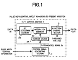
- Fig. 1 is a block drawing showing a basic structure of the pulse width control circuit of the present invention.
- the basic structure of the pulse width control circuit comprises a control signal generating section 1 generating a Tr/Tf control signal Sc for controlling pulse width of an input signal DATA_IN according to pulse width control information, a Tr/Tf control section 2 controlling one or both of a rise time Tr and a fall time Tf of the input signal DATA_IN according to the Tr/Tf control signal Sc, and a waveform shaping section 3 shaping a signal from the Tr/Tf control section 2 to output an output signal DATA_OUT.
- the Tr/Tf control section 2 includes a current source 2A, a bit detection element 2B and an integrating element 2C.
- the current source 2A generates a constant current in accordance with the Tr/Tf control signal Sc sent from the control signal generating section 1, to supply the constant current to the integrating element 2C.
- the bit detection element 2B is a circuit that detects whether each bit shown by the input signal DATA_IN is "HI” or "LOW", and transmits a detection result to the integrating element 2C.
- the integrating circuit 2C is a circuit that determines rise and fall time constants of the input signal DATA_IN based on the detection result of the bit detection element 2B and the constant current supplied from the current source 2A. An output signal of the integrating circuit 2C is sent to the waveform shaping section 3.
- Fig. 2 is a diagram for explaining the operating principle of the present pulse width control circuit
- a waveform example in the case where the pulse width is set to be wide is shown on the left
- a waveform example in the case where the pulse width is set to be narrow is shown on the right.
- the Tr/Tf control signal Sc for delaying, for example, the fall time Tf of the input signal DATA_IN according to a bit rate, is generated to be sent to the Tr/Tf control section 2.
- the rise time Tr of the input signal DATA_IN may be advanced according to the bit rate, or alternatively, the fall time Tf may be delayed while the rise time Tr being advanced according to the bit rate.
- Tr/Tf control section 2 there is performed a control for delaying the fall time Tf of the input signal DATA_IN according to the bit rate, in accordance with the Tr/Tf control signal Sc.
- the current source 2A is controlled in accordance with the Tr/Tf control signal Sc, so that the fall time constant of the input signal DATA_IN in the integrating element 2C is determined according to the bit rate.
- the Tr/Tf control signal Sc for delaying, for example, the rise time Tr of the input signal DATA_IN according to the bit rate, is generated to be sent to the Tr/Tf control section 2.
- the fall time Tf of the input signal DATA_IN may be advanced according to the bit rate, or alternatively, the fall time Tf may be advanced while the rise time Tr being delayed according to the bit rate.
- Tr/Tf control section 2 there is performed a control for delaying the rise time Tr of the input signal DATA_IN, according to the bit rate, in accordance with the Tr/Tf control signal Sc.
- the current source 2A is controlled in accordance with the Tr/Tf control signal Sc, so that the rise time constant of the input signal DATA_IN in the integrating element 2C is determined according to the bit rate.
- the rise time Tr and the fall time Tf of the input signal DATA_IN is controlled according to the bit rate. Then, even if the bit rate is changed, it is possible to primarily determine a pulse width adjustment amount, thus enabling to respond to multi-bit rates.
- Fig. 3 is a diagram showing an example of a specific circuit structure of the Tr/Tf control section.
- the Tr/Tf control section 2 is of a simple circuit structure provided with, for example, two current sources I1 and I2 as the current source 2A, a P-channel MOSFET tp1 and an N-channel MOSFET tn1 as the bit detection element 2B, and two P-channel MOSFETs tp2 and tp3 and two N-channel MOSFETs tn2 and tn3 as the integrating element 2C.
- the current source I1 has one terminal connected to a power source V and the other terminal connected to a drain terminal of the N-channel MOSFET tn1, and a current value thereof is controlled in accordance with the Tr/Tf control signal Sc from the control signal generating section 1.
- the current source I2 has one terminal grounded and the other terminal connected to a drain terminal of the P-channel MOSFET tp1, and a current value thereof is controlled in accordance with the Tr/Tf control signal Sc from the control signal generating section 1.
- Specific current sources I1 and I2 can be made up of current mirror circuits, to which the current from the control signal generating section 1 is input, in the case where a current of a required value is output from the control signal generating circuit 1 as the Tr/Tf control signal Sc, for example,.
- the P-channel MOSFET tp1 as the bit detection element 2B has a gate terminal connected to an input terminal of the Tr/Tf control section 2, and a source terminal connected to the power source V.
- the N-channel MOSFET tn1 has a gate terminal connected to the input terminal of the Tr/Tf control section 2 and a source terminal grounded.
- the P-channel MOSFET tp2 has a drain terminal and a gate terminal each connected to the current source 12, and a source terminal connected to the power source V.
- the N-channel MOSFET tn2 has a drain terminal and a gate terminal each connected to the current source I1 and a source terminal grounded.
- the P-channel MOSFET tp3 has a source terminal connected to the power source V, a gate terminal connected to the current source 12, and a drain terminal connected to an output terminal of the Tr/Tf control section 2.
- the N-channel MOSFET tn3 has a source terminal grounded, a gate terminal connected to the current source I1, and a drain terminal connected to the output terminal of the Tr/Tf control section 2.
- the current source I2 is adjusted in order to control the rise time Tr of the input signal DATA_IN, while the current source 11 being adjusted in order to control the fall time Tf.
- Fig. 5 is a diagram showing an example of the specific circuit structure of the Tr/Tf control section to improve noise resistance.
- a difference between a structure of a Tr/Tf control section 2' of Fig. 5 and the Tr/Tf control section 2 of Fig. 3 is in that a P-channel MOSFET tp2' and an N-channel MOSFET tn2' are added to the integrating element 2C.
- the P-channel MOSFET tp2' has a drain terminal and a gate terminal each connected to the source terminal of the P-channel MOSFET tp2, and a source terminal connected to the power source V.
- the N-channel MOSFET tn2' has a drain terminal and a gate terminal each connected to the source terminal of the N-channel MOSFET tn2, and a source terminal grounded.
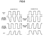
- Tr/Tf control section 2' A basic operation of the above Tr/Tf control section 2' is the same as that of the Tr/Tf control section 2 of Fig. 3 described above. However, since the P-channel MOSFET tp2' and the N-channel MOSFET tn2' are connected so that amplitudes of voltage signals in points A and B shown in the second and third levels from the top in Fig. 6 become large, resistance of the Tr/Tf control section 2' to power source noise and ground noise is improved.
- Fig. 7 is a diagram showing a specific circuit structure of the modification example of the Tr/Tf control section of Fig. 3.
- a Tr/Tf control section 2 instead of the current sources I1 and I2 in the Tr/Tf control section 2 of Fig. 3, there are provided two P-channel MOSFETs tp4 and tp5 constituting a first current mirror circuit to which the Tr/Tf control signal Sc is input from the control signal generating section 1, two N-channel MOSFETs tn4 and tn5 constituting a second current mirror circuit to which an output signal of the first current mirror circuit is input, and a current source I3 and a N-channel MOSFET tn6 connected to the current source 13.
- Constitutions other than those described above, that is, the constitutions of the bit detection element 2B and the integrating element 2C are the same as those of the Tr/Tf control section 2 of Fig. 3. Further, these constitutions may be the same as those of the Tr/Tf control section 2' of Fig. 5.
- the P-channel MOSFET tp4 constituting the first current mirror circuit has a source terminal connected to the power source V, and a commonly connected drain terminal and a gate terminal, to which the Tr/Tf control signal Sc is input from the control signal generating section 1. Further, the P-channel MOSFET tp5 has a source terminal connected to the power source V, a gate terminal connected to the gate terminal of the P-channel MOSFET tp4, and a drain terminal connected to the second current mirror circuit.
- the N-channel MOSFET tn4 constituting the second current mirror circuit has a source terminal grounded, and a commonly connected drain terminal and a gate terminal, to which a current from the first current mirror circuit is input. Further, the N-channel MOSFET tn5 has a source terminal grounded, a gate terminal connected to the gate terminal of the N-channel MOSFET tn4, and a drain terminal connected to the drain terminal of the P-channel MOSFET tp1 of the bit detection element 2B.
- the current source I3 has one terminal connected to the power source V, and the other terminal connected to the drain terminals of the N-channel MOSFETs tn1 and tn6.
- the N-channel MOSFET tn6 has a gate terminal connected to an output of the first current mirror circuit, that is, the drain terminal of the P-channel MOSFET tp5, and a source terminal grounded.
- the current source I3 and the N-channel MOSFET tn6 correspond to the current source 11 of the Tr/Tf control section 2 of Fig. 3
- the N-channel MOSFET tn5 output current from the second current mirror circuit
- Tr/Tf control section 2 a current of a desired value is input to the first current mirror circuit, as the Tr/Tf control signal Sc from the control signal generating section 1, so that a current flows to each part in accordance with a relationship shown in Fig. 8.
- Tr/Tf control signal Sc represents a level of the Tr/Tf control signal Sc, that is, a value of the current input to the first current mirror circuit, and the ordinate represents a current la flowing through the P-channel MOSFET tp4, a current Ib flowing through the P-channel MOSFET tp5, a current Id flowing through the N-channel MOSFET tn6, a current I1 flowing through the drain point of the N-channel MOSFET tn1, and a current I2 flowing through the drain point of the P-channel MOSFET tp1.
- the Tr/Tf control signal Sc may be appropriately set so that the values of the currents I1 and I2 become desired values according to the bit rate.
- Fig. 9 shows another specific structural example of the Tr/Tf control section.
- the current source 2A comprises current output D/A converters (IDACs) 21 and 22 controlled by signals from a CPU 4.
- a memory 4A comprising a ROM, a non-volatile memory or the like, and a temperature sensor 4B detecting the surrounding temperature, are connected to the CPU 4.
- Signals for controlling the current output D/A converters 21 and 22 are generated by the CPU 4, based on pulse width control information supplied from exterior, information stored in the memory 4A, and the detection result of the temperature sensor 4B. Consequently, when the present Tr/Tf control section 2"' is used, a function corresponding to the control signal generating section 1 is realized by the CPU 4, the memory 4A, and the temperature sensor 4B.
- the constitutions of the bit detection element 2B and the integrating element 2C are the same as those of the Tr/Tf control section 2 of Fig. 3.
- the stored information of the memory 4A is read out by the CPU 4 according to the pulse width control information from exterior and the detection result of the temperature sensor 4B, and the signal for controlling each of the current output D/A converters 21 and 22 is generated.
- a corresponding relationship between an LD turn-on delay time and the pulse width control information is previously stored in the memory 4A, and also, as LD temperature characteristic information, information relating to temperature characteristic with regard to a threshold current Ith, a modulated current Ip and a bias current Ib of the LD are previously stored in the memory 4A.
- the LD turn-on delay time is calculated in accordance with the equation (1) described above, using the LD temperature characteristic information corresponding to the detection result of the temperature sensor 4B, and based on the corresponding relationship between the turn-on delay time and the pulse width control information, the current values of the current output D/A converters 21 and 22 are controlled so as to realize the rise time Tr and the fall time Tf corresponding to the bit rate. Then, the currents generated by the current output D/A converters 21 and 22 flow through the drain points of the P-channel MOSFET tp1 and the N-channel MOSFET tn1, thereby, similarly to the case of the Tr/Tf control section 2 of Fig. 3 described above, the rise time Tr and fall time Tf of the input signal DATA_IN are controlled. Thus, it becomes possible to realize an automatic control of the pulse width according to the LD temperature characteristic.
- the circuit example shown in Fig. 9 described above has been constituted to use the current output D/A converters.
- the constitution may be such that voltage output D/A converters controlled by the CPU 4, for example, are used, and a circuit for converting an output voltage of each of the voltage output D/A converters to a current is provided.
- the constitution has been such that the pulse width control information from exterior is sent to the CPU 4, it is also possible to previously store the pulse width control information in the memory 4A.
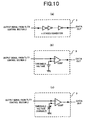
- Fig. 10 is a diagram that enumerates specific circuit structure examples of the waveform shaping section 3.
- the circuit structure of (a) in Fig. 10 is one example in which the waveform shaping section 3 is formed by inverters of n-stages to which a signal from the Tr/Tf control section 2 is input.
- the output signal DATA_OUT of the waveform shaping section 3 has a pulse width narrower than that of the input signal DATA_IN of the pulse width control circuit.
- the rise time Tr of the input signal of the waveform shaping section 3 is advanced, while the fall time Tf being delayed, the output signal DATA_OUT of the waveform shaping section 3 has a pulse width wider than that of the input signal DATA_IN of the pulse width control circuit.
- the circuit structure of (b) in Fig. 10 is an example in which the waveform shaping section 3 is formed by a comparator (COMP) to which a signal from the Tr/Tf control section 2 is input as a forward input (or inversion input), and the threshold voltage generated at the constant voltage source is input as the inversion input (or the forward input).
- the circuit structure of (c) of Fig. 10 is a circuit that enables the threshold voltage input to the comparator to be adjusted from exterior, thereby capable to further widen a pulse width control range.
- Fig. 11 is a diagram that enumerates specific circuit structure examples of the control signal generating section 1.
- the circuit structure of (a) in Fig. 11 is an example in which the control signal generating section 1 is formed using: a constant current source 1A and a variable resistor 1 B connected in series between the power source and ground; an operational amplifier 1C with one input terminal connected to a common connection point of the constant current source 1A and the variable resistor 1B; an N-channel MOSFET tn7 having a gate terminal connected to an output terminal of the operational amplifier 1C, a source terminal connected the other input terminal of the operational amplifier 1 C, and a drain terminal connected to an output terminal of the control signal generating section 1; and a resistor 1 D having one terminal connected to the source terminal of the N-channel MOSFET tn7 and the other terminal grounded.
- a current output as the Tr/Tf control signal Sc can be controlled to a desired value by adjusting a resistance value of the variable resistor 1 B according to the pulse width control
- circuit structure of (b) of Fig. 11 is an example in which the control signal generating section 1 is formed, by providing a constant voltage source 1 E instead of the above constant current source 1A and variable resistor 1B, and a variable resistor 1F instead of the resistor 1D.
- a current output as the Tr/Tf control signal Sc can be controlled to a desired value by adjusting a resistance value of the variable resistor 1 F according to the pulse width control information.
- control signal generating section 1 such a constitution as shown in Fig. 9 comprising the CPU 4, memory 4A and temperature sensor 4B may be used.
- a current output D/A converter or the like is used as the current source 2A of the Tr/Tf control section 2.
- a thermistor or the like is provided instead of the resistor 1 D in the circuit structure of (a) in Fig. 11, and a constant current source and a thermistor or the like connected in series between the power source and ground are provided instead of the constant voltage source 1 E in the circuit structure of (b) of Fig. 11, so that the Tr/Tf control signal Sc is generated according to a change in the ambient temperature.
- the constitution may be such that the Tr/Tf control sections 2 and waveform shaping sections 3 are connected in multi-stages, to adjust the pulse width of the input signal DATA_IN in stepwise.
- the pulse width is set to be wide, since the band restriction in the Tr/Tf control section 2 of each stage can be suppressed to a small range, the noise resistance at each stage can be improved, and consequently, it is possible to improve the noise resistance of the overall pulse width control circuit.
- by suppressing an adjustment range of the pulse width at each stage to be small it is also possible to suppress a pattern effect at each stage.
- Tr/Tf control sections 2 and the waveform shaping sections 3 are connected in multi-stages, it becomes possible to achieve effects, such as extension of the applied bit rate range, extension of the pulse width control range, suppression of pattern effect, improvement of electrical and ground noise resistances, and the like.
- the pulse width control circuit of the present invention since one or both of the rise time Tr and fall time Tf of the input signal DATA_IN is variable controlled according to the bit rate, it is possible to easily realize the response to multi-bit rates. Further, since the Tr/Tf control sections 2 and the waveform shaping sections 3 are connected in multi-stages, it is possible to make the bit rate range wider. Specifically, it is possible to perform the pulse width control in a bit rate range of on the order of 50Mbps to 2.4Gbps.
- the present pulse width control circuit is not a type of controlling the pulse width by changing the threshold voltage (slice level) in the waveform shaping section 3 as in the conventional technique, but is basically a type of variably controlling the rise time Tr and fall time Tf of the input signal DATA_IN it is possible to improve the resistance to electrical noise and ground noise.
- this pulse width control circuit since a DC voltage at point A in Fig. 1 is changed according to the power source voltage, and the on/off speed of the P-channel MOSFET tp3 is changed according to the power source voltage, the output signal DATA_OUT is not liable to be affected by power source voltage fluctuation. Consequently, compared to the conventional circuits, pulse width fluctuation due to power source voltage fluctuation can be suppressed.
- the pulse width control circuit of the present invention can be constituted by a number of MOSFETs. Therefore, the pulse width control circuit of the present invention does not affect on the chip size of LSIs, and is effective in the reduction of the chip surface area and the reduction of cost.
- the present invention in fields such as optical communications and the like, has considerable industrial applicability as an electrical circuit technology for controlling the pulse width of data signals to be used in the drive circuits of light emitting elements.
Landscapes
- Physics & Mathematics (AREA)
- Engineering & Computer Science (AREA)
- Computer Networks & Wireless Communication (AREA)
- Signal Processing (AREA)
- Electromagnetism (AREA)
- Spectroscopy & Molecular Physics (AREA)
- Power Engineering (AREA)
- Nonlinear Science (AREA)
- Pulse Circuits (AREA)
- Logic Circuits (AREA)
- Led Devices (AREA)
Abstract
Description
Claims (13)
- A pulse width control circuit for controlling pulse width of an input signal based on pulse width control information, and generating an output signal for driving a light emitting element, comprising:a rise/fall control section controlling at least one of a rise time and a fall time of said input signal according to a bit rate of said input signal;a waveform shaping section shaping a signal output from said rise/fall control section, to generate said output signal; anda control signal generating section generating a control signal for controlling an operation of said rise/fall control section based on said pulse width control information.
- A pulse width control circuit according to claim 1,
wherein said rise/fall control section comprises:a current source controlled in accordance with the control signal from said control signal generating section;a bit detection element detecting a level of each bit indicated by said input signal; andan integrating element determining rise and fall time constants of said input signal based on a current supplied from said current source and detection results from said bit detection element. - A pulse width control circuit according to claim 2,
wherein said current source includes: a first current source having one terminal applied with a power source voltage, a current value thereof being controlled in accordance with the control signal from said control signal generating section; and a second current source having one terminal grounded, a current value thereof being controlled in accordance with the control signal from said control signal generating section;said bit detection element includes: a P-channel MOSFET having a gate terminal applied with said input signal, a source terminal applied with the power source voltage, and a drain terminal connected to the other terminal of said second current source; and an N-channel MOSFET having a gate terminal applied with said input signal, a source terminal grounded, and a drain terminal connected to the other terminal of said first current source; andsaid integrating circuit includes: a first P-channel MOSFET having a drain terminal and a gate terminal each connected to the other terminal of said second current source, and a source terminal applied with the power source voltage; a first N-channel MOSFET having a drain terminal and a gate terminal each connected to the other terminal of said first current source, and a source terminal grounded; a second P-channel MOSFET having a gate terminal connected to the other terminal of said second current source, a source terminal applied with the power source voltage, and a drain terminal connected to an output terminal of said rise/fall control section; and a second N-channel MOSFET having a gate terminal connected to the other terminal of said first current source, a source terminal grounded, and a drain terminal connected to the output terminal of said rise/fall control section. - A pulse width control circuit according to claim 3,
wherein said integrating element includes: a third P-channel MOSFET having a drain terminal and a gate terminal each connected to the source terminal of said first P-channel MOSFET, and a source terminal applied with the power source voltage; and a third N-channel MOSFET having a drain terminal and a gate terminal each connected to the source terminal of said first N-channel MOSFET, and a source terminal grounded. - A pulse width control circuit according to claim 2,
wherein said current source includes: a first current mirror circuit that is input with the control signal from said control signal generating section; a second current mirror circuit that is input with an output signal of said first current mirror circuit; a third current source having one terminal input with a power source voltage; and an N-channel MOSFET having a gate terminal applied with the output signal of said first current mirror circuit, a drain terminal connected to the other terminal of said third current source, and a source terminal grounded;said bit detection element includes: a P-channel MOSFET having a gate terminal applied with said input signal, a source terminal applied with the power source voltage, and a drain terminal connected to an output terminal of said second current mirror circuit; and an N-channel MOSFET having a gate terminal applied with said the input signal, a source terminal grounded, and a drain terminal connected to the other terminal of said third current source; andsaid integrating element includes a first P-channel MOSFET having a drain terminal and a gate terminal each connected to the output terminal of said second current mirror circuit, and a source terminal applied with the power source voltage; a first N-channel MOSFET having a drain terminal and a gate terminal each connected to the other terminal of the third current source, and a source terminal grounded; a second P-channel MOSFET having a gate terminal connected to the output terminal of said second current mirror circuit, a source terminal applied with the power source voltage, and a drain terminal connected to an output terminal of said rise/fall control section; and a second N-channel MOSFET having a gate terminal connected to the other terminal of the third current source, a source terminal grounded, and a drain terminal connected to the output terminal of said rise/fall control section. - A pulse width control circuit according to claim 2,
wherein said current source is constituted by a current output D/A converter, and said control signal generating section generates a control signal for controlling said current output D/A converter. - A pulse width control circuit according to claim 1,
wherein said waveform shaping section is constituted by an inverter circuit that is input with a signal output from said rise/fall control section. - A pulse width control circuit according to claim 1,
wherein said waveform shaping section is constituted by a voltage source generating a previously set threshold voltage, and a converter having one input terminal applied with a signal output from said rise/fall control section, and the other input terminal applied the threshold voltage generated by said voltage source. - A pulse width control circuit according to claim 8,
wherein said voltage source generates a variable threshold voltage. - A pulse width control circuit according to claim 1,
wherein said control signal generating section includes a variable resistor with a resistance value thereof being controlled based on said pulse width control information, and a current controlled according to the resistance value of said variable resistor, is output as a control signal for controlling an operation of said rise/fall control section. - A pulse width control circuit according to claim 1,
wherein said control signal generating section includes a temperature sensor detecting a temperature, and generates a control signal for controlling an operation of said rise/fall control section based on a detection result of said temperature sensor, and said pulse width control information. - A pulse width control circuit according to claim 1,
wherein said control signal generating section includes a memory previously storing said pulse width control information, and generates a control signal controlling an operation of said rise/fall control section based on the pulse width control information in said memory. - A pulse width control circuit according to claim 1,
wherein a plurality of units each constituted by said rise/fall control section and said waveform shaping section are connected in multi-stages, and an operation of said rise/fall control section of each unit is controlled according to a control signal generated by said control signal generating section.
Applications Claiming Priority (1)
| Application Number | Priority Date | Filing Date | Title |
|---|---|---|---|
| PCT/JP2000/007519 WO2002035740A1 (en) | 2000-10-26 | 2000-10-26 | Pulse width control circuit |
Publications (3)
| Publication Number | Publication Date |
|---|---|
| EP1330051A1 true EP1330051A1 (en) | 2003-07-23 |
| EP1330051A4 EP1330051A4 (en) | 2006-04-12 |
| EP1330051B1 EP1330051B1 (en) | 2009-12-16 |
Family
ID=11736627
Family Applications (1)
| Application Number | Title | Priority Date | Filing Date |
|---|---|---|---|
| EP00970112A Expired - Lifetime EP1330051B1 (en) | 2000-10-26 | 2000-10-26 | Pulse width control circuit |
Country Status (5)
| Country | Link |
|---|---|
| US (2) | US6700423B1 (en) |
| EP (1) | EP1330051B1 (en) |
| JP (1) | JP3733116B2 (en) |
| DE (1) | DE60043550D1 (en) |
| WO (1) | WO2002035740A1 (en) |
Cited By (1)
| Publication number | Priority date | Publication date | Assignee | Title |
|---|---|---|---|---|
| GB2397478B (en) * | 2003-01-16 | 2007-03-14 | Agilent Technologies Inc | Communication module and related method |
Families Citing this family (8)
| Publication number | Priority date | Publication date | Assignee | Title |
|---|---|---|---|---|
| US7271635B2 (en) * | 2004-07-15 | 2007-09-18 | Micron Technology | Method and apparatus for reducing duty cycle distortion of an output signal |
| CN1735081B (en) * | 2004-08-11 | 2010-10-06 | 华为技术有限公司 | Control method and circuit for output signal waveform of line driver |
| EP1841668B1 (en) * | 2005-01-14 | 2009-04-22 | Graphic Packaging International, Inc. | Package for browning and crisping dough-based foods in a microwave oven |
| JP2006217172A (en) * | 2005-02-02 | 2006-08-17 | Sanyo Electric Co Ltd | Delay circuit and ring oscillator |
| JP4670675B2 (en) * | 2006-02-16 | 2011-04-13 | ソニー株式会社 | Drive circuit for charge transfer unit and drive method for charge transfer unit |
| US8344777B2 (en) * | 2010-02-24 | 2013-01-01 | Intersil Americas Inc. | Method and apparatus for adaptively modifying a pulse width of a pulse width modulated output |
| JP7102728B2 (en) * | 2017-12-26 | 2022-07-20 | 富士フイルムビジネスイノベーション株式会社 | Laser drive control device, drying device, image forming device, laser drive control program and drying program |
| CN108983860B (en) * | 2018-09-18 | 2024-01-12 | 杭州洪芯微电子科技有限公司 | Current self-checking regulating circuit based on voltage calibration |
Family Cites Families (17)
| Publication number | Priority date | Publication date | Assignee | Title |
|---|---|---|---|---|
| JPS6230433A (en) * | 1985-08-01 | 1987-02-09 | Oki Electric Ind Co Ltd | Laser diode bias current control system |
| JPH01314013A (en) * | 1988-06-11 | 1989-12-19 | Sony Corp | Duty ratio variable circuit |
| JP2539667Y2 (en) * | 1988-06-15 | 1997-06-25 | ソニー株式会社 | Variable duty circuit |
| DE3885750D1 (en) * | 1988-09-26 | 1993-12-23 | Siemens Ag | CMOS pulse width modulator. |
| US5081380A (en) * | 1989-10-16 | 1992-01-14 | Advanced Micro Devices, Inc. | Temperature self-compensated time delay circuits |
| JP2864596B2 (en) * | 1989-12-21 | 1999-03-03 | 日本電気株式会社 | Laser diode drive circuit |
| JPH06169237A (en) * | 1991-09-13 | 1994-06-14 | Mitsubishi Electric Corp | Ring oscillator circuit |
| JPH07141865A (en) * | 1993-06-28 | 1995-06-02 | Mitsubishi Electric Corp | Oscillation circuit and semiconductor memory device |
| US6462598B1 (en) * | 1996-10-28 | 2002-10-08 | Advantest Corp. | Delay time control circuit |
| US5994937A (en) * | 1996-11-06 | 1999-11-30 | International Business Machines Corporation | Temperature and power supply adjusted address transition detector |
| JPH10242915A (en) | 1997-02-26 | 1998-09-11 | Fujitsu Ltd | Optical transmitter |
| US6169765B1 (en) * | 1997-05-28 | 2001-01-02 | Integration Associates, Inc. | Apparatus and method for output signal pulse width error correction in a communications receiver |
| JP3839577B2 (en) * | 1998-03-11 | 2006-11-01 | 富士通株式会社 | Semiconductor laser drive circuit |
| JP3473400B2 (en) * | 1998-05-19 | 2003-12-02 | 松下電器産業株式会社 | Oscillator |
| JPH11340927A (en) * | 1998-05-27 | 1999-12-10 | Nec Corp | Pulse width adjustment circuit and semiconductor laser driving circuit |
| JP2000013204A (en) * | 1998-06-18 | 2000-01-14 | Fujitsu Ltd | Delay circuit and oscillation circuit using the delay circuit |
| JP3644010B2 (en) * | 1999-03-29 | 2005-04-27 | 富士通株式会社 | Optical transmission circuit |
-
2000
- 2000-10-26 EP EP00970112A patent/EP1330051B1/en not_active Expired - Lifetime
- 2000-10-26 WO PCT/JP2000/007519 patent/WO2002035740A1/en not_active Ceased
- 2000-10-26 DE DE60043550T patent/DE60043550D1/en not_active Expired - Lifetime
- 2000-10-26 JP JP2002538595A patent/JP3733116B2/en not_active Expired - Fee Related
-
2003
- 2003-01-15 US US10/342,251 patent/US6700423B1/en not_active Expired - Fee Related
-
2004
- 2004-01-12 US US10/754,703 patent/US6940327B2/en not_active Expired - Fee Related
Cited By (1)
| Publication number | Priority date | Publication date | Assignee | Title |
|---|---|---|---|---|
| GB2397478B (en) * | 2003-01-16 | 2007-03-14 | Agilent Technologies Inc | Communication module and related method |
Also Published As
| Publication number | Publication date |
|---|---|
| JP3733116B2 (en) | 2006-01-11 |
| EP1330051B1 (en) | 2009-12-16 |
| US20040251943A1 (en) | 2004-12-16 |
| JPWO2002035740A1 (en) | 2004-03-04 |
| US6940327B2 (en) | 2005-09-06 |
| US6700423B1 (en) | 2004-03-02 |
| WO2002035740A1 (en) | 2002-05-02 |
| DE60043550D1 (en) | 2010-01-28 |
| EP1330051A4 (en) | 2006-04-12 |
Similar Documents
| Publication | Publication Date | Title |
|---|---|---|
| EP0845863B1 (en) | Pulse-width controller | |
| EP0744800B1 (en) | Laser-diode driving circuit | |
| US6826215B2 (en) | Laser diode driving circuit | |
| EP1330051B1 (en) | Pulse width control circuit | |
| US9130341B2 (en) | Semiconductor laser drive apparatus and image forming apparatus | |
| JP4566692B2 (en) | LIGHT EMITTING DIODE DRIVING DEVICE AND OPTICAL TRANSMISSION DEVICE HAVING THE SAME | |
| US7595645B2 (en) | Calibration circuit and semiconductor device incorporating the same | |
| US7068691B2 (en) | Directly modulated optical module and method for driving semiconductor laser included therein | |
| US20030042940A1 (en) | Driver circuit | |
| US7812587B2 (en) | LED drive circuit | |
| US5708673A (en) | Optical signal transmitter | |
| JP4339208B2 (en) | Data driving circuit and semiconductor device using the same | |
| JPH10224188A (en) | Output pulse width control system | |
| JPH04283978A (en) | Laser diode drive circuit | |
| US6373297B1 (en) | Input buffer capable of achieving quick response | |
| US5309463A (en) | Laser driving circuit | |
| US20050259375A1 (en) | Overcurrent protection circuit | |
| JP2006047039A (en) | Temperature detection circuit and power semiconductor device provided with temperature detection circuit | |
| US7155474B2 (en) | Current-mode multi-valued full adder in semiconductor device | |
| EP3772821B1 (en) | An electric circuit, a method for generating a pulse width modulated output signal, and a control system for a time-of-flight camera | |
| KR20000067250A (en) | Charge pump circuit and pll employing therefor | |
| US7471108B2 (en) | Variable reference level input circuit and method | |
| WO2024043129A1 (en) | Light source device and ranging device | |
| JPH11340927A (en) | Pulse width adjustment circuit and semiconductor laser driving circuit | |
| JP2008263071A (en) | Drive current control circuit and light emitting element drive circuit |
Legal Events
| Date | Code | Title | Description |
|---|---|---|---|
| PUAI | Public reference made under article 153(3) epc to a published international application that has entered the european phase |
Free format text: ORIGINAL CODE: 0009012 |
|
| 17P | Request for examination filed |
Effective date: 20030326 |
|
| AK | Designated contracting states |
Designated state(s): AT BE CH CY DE DK ES FI FR GB GR IE IT LI LU MC NL PT SE |
|
| RBV | Designated contracting states (corrected) |
Designated state(s): DE FR GB |
|
| A4 | Supplementary search report drawn up and despatched |
Effective date: 20060224 |
|
| RIC1 | Information provided on ipc code assigned before grant |
Ipc: H04L 25/02 20060101ALI20020504BHEP Ipc: H03K 5/04 20060101ALI20020504BHEP Ipc: H04B 10/155 20060101AFI20060220BHEP Ipc: H01S 5/062 20060101ALI20020504BHEP |
|
| 17Q | First examination report despatched |
Effective date: 20061109 |
|
| GRAP | Despatch of communication of intention to grant a patent |
Free format text: ORIGINAL CODE: EPIDOSNIGR1 |
|
| GRAS | Grant fee paid |
Free format text: ORIGINAL CODE: EPIDOSNIGR3 |
|
| RIN1 | Information on inventor provided before grant (corrected) |
Inventor name: MIKI, MAKOTO,FUJITSU HIGASHI-NIHON DIGITAL Inventor name: MATSUYAMA, TORU,FUJITSU HIGASHI-NIHON DIGITAL |
|
| GRAA | (expected) grant |
Free format text: ORIGINAL CODE: 0009210 |
|
| AK | Designated contracting states |
Kind code of ref document: B1 Designated state(s): DE FR GB |
|
| REG | Reference to a national code |
Ref country code: GB Ref legal event code: FG4D |
|
| REF | Corresponds to: |
Ref document number: 60043550 Country of ref document: DE Date of ref document: 20100128 Kind code of ref document: P |
|
| PLBE | No opposition filed within time limit |
Free format text: ORIGINAL CODE: 0009261 |
|
| STAA | Information on the status of an ep patent application or granted ep patent |
Free format text: STATUS: NO OPPOSITION FILED WITHIN TIME LIMIT |
|
| 26N | No opposition filed |
Effective date: 20100917 |
|
| PG25 | Lapsed in a contracting state [announced via postgrant information from national office to epo] |
Ref country code: FR Free format text: LAPSE BECAUSE OF NON-PAYMENT OF DUE FEES Effective date: 20101102 |
|
| REG | Reference to a national code |
Ref country code: FR Ref legal event code: ST Effective date: 20110630 |
|
| REG | Reference to a national code |
Ref country code: DE Ref legal event code: R119 Ref document number: 60043550 Country of ref document: DE Effective date: 20110502 |
|
| PG25 | Lapsed in a contracting state [announced via postgrant information from national office to epo] |
Ref country code: DE Free format text: LAPSE BECAUSE OF NON-PAYMENT OF DUE FEES Effective date: 20110502 |
|
| PGFP | Annual fee paid to national office [announced via postgrant information from national office to epo] |
Ref country code: GB Payment date: 20141022 Year of fee payment: 15 |
|
| GBPC | Gb: european patent ceased through non-payment of renewal fee |
Effective date: 20151026 |
|
| PG25 | Lapsed in a contracting state [announced via postgrant information from national office to epo] |
Ref country code: GB Free format text: LAPSE BECAUSE OF NON-PAYMENT OF DUE FEES Effective date: 20151026 |