EP1330023A2 - Direct conversion receiver architecture - Google Patents
Direct conversion receiver architecture Download PDFInfo
- Publication number
- EP1330023A2 EP1330023A2 EP03250300A EP03250300A EP1330023A2 EP 1330023 A2 EP1330023 A2 EP 1330023A2 EP 03250300 A EP03250300 A EP 03250300A EP 03250300 A EP03250300 A EP 03250300A EP 1330023 A2 EP1330023 A2 EP 1330023A2
- Authority
- EP
- European Patent Office
- Prior art keywords
- receiver
- input
- coupled
- operational amplifier
- base band
- Prior art date
- Legal status (The legal status is an assumption and is not a legal conclusion. Google has not performed a legal analysis and makes no representation as to the accuracy of the status listed.)
- Granted
Links
Images




Classifications
-
- H—ELECTRICITY
- H04—ELECTRIC COMMUNICATION TECHNIQUE
- H04B—TRANSMISSION
- H04B1/00—Details of transmission systems, not covered by a single one of groups H04B3/00 - H04B13/00; Details of transmission systems not characterised by the medium used for transmission
- H04B1/06—Receivers
- H04B1/16—Circuits
- H04B1/30—Circuits for homodyne or synchrodyne receivers
-
- H—ELECTRICITY
- H03—ELECTRONIC CIRCUITRY
- H03G—CONTROL OF AMPLIFICATION
- H03G3/00—Gain control in amplifiers or frequency changers
- H03G3/20—Automatic control
- H03G3/30—Automatic control in amplifiers having semiconductor devices
- H03G3/3052—Automatic control in amplifiers having semiconductor devices in bandpass amplifiers (H.F. or I.F.) or in frequency-changers used in a (super)heterodyne receiver
Definitions
- RF radio frequency
- IFs intermediate frequencies
- the mobile station In modem wireless communications systems, in particular cellular telecommunications systems, the mobile station (also referred to, for example, as a wireless terminal or as a cellular telephone) must perform a number of tasks that are commanded by the base station. One of these tasks is to receive and measure the power level of different radio channels, such as those originating in neighbor cells, and to report the results of the measurements back to the base station.
- the MS may be required to tune its receiver from a current channel to a channel to be measured, make the measurement, and then tune back to the original channel in order to continue an ongoing communication or to listen for a page.
- a multi-band receiver is one that is capable of operating with at least two communication frequency bands (e.g., 1900 MHz and 800MHz). If a multi-band receiver uses a common base band circuit for all the frequency bands, it is even more crucial to quickly recover from the channel measurement task. This is particularly the case if, for example, burst-type GSM (Global System for Mobile Communications) channels are required to be measured while a WCDMA (Wideband Code Division Multiple Access) call is in progress.
- GSM Global System for Mobile Communications
- WCDMA Wideband Code Division Multiple Access
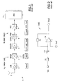
- Fig. 1 shows a conventional architecture for a direct conversion receiver 1 having a front end 1A and a base band section 1B.
- RF signals are received through an antenna 2, amplified in a low noise amplifier (LNA) stage 3 and downconverted to baseband in a mixer stage 4, using a local oscillator input.
- the base band section 1B includes a base band gain block 5, a channel selection filter 6, an automatic gain control (AGC) block 7 and an analog to digital converter (ADC) 8 where the received signal is converted into digital data for subsequent processing in the digital domain.
- LNA low noise amplifier
- ADC analog to digital converter
- the largest time constants of the direct conversion receiver 1 can typically be found in the AGC block 7.
- the limiting factor on the other channel measurement task is typically related to the magnitude of the time constants inherent in the operation of the AGC block 7.
- the AGC block 7 includes an amplifier 7A (shown connected in an inverting configuration), input resistor R1, feedback resistor R2 and an input DC blocking capacitor C1.
- the DC-voltage of the output must be set to a proper value by using the DC compensation circuit of the AGC block 7.
- this circuit normally contains large capacitors (e.g., C1), which have to be charged to a proper value before reception. The charging of the capacitors requires some finite amount of time and also consumes current.
- a further problem in the conventional direct conversion receiver relates to the biasing of the base band section 1B.
- the lowest signal frequency in the base band is 0Hz (i.e, DC)
- care must be taken to avoid the occurrence of the wrong biasing of the base band section 1B when the gain is changed. This requirement results in the use of DC-compensation circuitry.
- the AGC circuitry 7 may not have the same gain for DC that it has for higher frequencies. This is true because the biasing of the base band section 1B may be changed each time the gain is changed. Providing a different value for the gain for operation at 0Hz (DC) has traditionally been achieved through the use of large AC-coupling capacitors. As was discussed above, these capacitors must be charged to the correct value before each reception burst (as in a Time Division Multiple Access (TDMA) system such as GSM). Normally the charging is performed in a situation where some undesired signal is also present in the system. Therefore it is possible that not only the DC-value is charged to the capacitor, but that some of the undesired signal appears as well. This occurrence can result in the generation of a large and undesirable offset in the output of the base band section 1B.
- TDMA Time Division Multiple Access
- Fig. 3 which corresponds to the R1/C1 input network shown in Fig. 2, in accordance with conventional practice the coupling capacitor (C) is charged as a 1 st order lowpass filter, resulting in the AC value of the incoming error signal being reduced.
- the first order lowpass filter of Fig. 3 does not decrease the signal sufficiently, as the lowpass comer frequency cannot be decreased without increasing the time constant of the circuit, and hence increasing the required DC-compensation time (which is limited by system timing constraints).
- the time constant of the AGC circuit is removed altogether, enabling the direct conversion receiver to be more quickly changed from one reception band to another. While reception can proceed as well in a conventional fashion, if no gain (or low gain) is required from the AGC circuit, the DC-compensation can be avoided.
- Disclosed is a method for operating a mobile station that includes an RF receiver having an RF front end followed by a base band section.
- the base band section includes an AGC block that contains a DC blocking capacitor coupled in series between an input node of the AGC block and an input to a gain element.
- the method has steps of tuning from a current RF channel to another RF channel to make a signal strength measurement, and reducing a time constant of the AGC circuit by shorting around the DC blocking capacitor.
- an AGC circuit that includes a first order low pass filter is provided with a switch and with additional components for operating with a second order low pass filter, thereby increasing the attenuation of the input AC signal.
- This method has steps of operating the AC coupling capacitance and the first resistance as a first order low pass filter for attenuating the AC value of an input signal, and closing at least one switch for switching in additional capacitance and resistance for transforming the first order low pass filter to a second order low pass filter for increasing the attenuation of the AC value of the input signal.
- a mobile station includes an RF receiver having an RF front end with an output coupled to an input of a base band section.
- the base band section includes an automatic gain control AGC block having a capacitance coupled between an input node of the AGC block and an input to a gain element, typically an operational amplifier.
- the AGC block further includes a plurality of switches controlled by a control unit of the mobile station, such as a DSP, for operating the AGC block in an all-pass signal reception made of operation, or in a first DC compensation mode of operation, where a signal appearing across the capacitance is low pass filtered with a first order filter, or in a second DC compensation mode of operation, where a signal appearing across the capacitance is low pass filtered with a second order filter.
- a control unit of the mobile station such as a DSP
- Circuit topologies are described for both inverting and non-inverting operational amplifier implementations.
- Fig. 4 where there is illustrated a simplified block diagram of an embodiment of a wireless communications system 5 that includes at least one mobile station (MS) 100 that is suitable for practicing this invention.
- Fig. 4 also shows an exemplary network operator having, for example, a GPRS Support Node (GSN) 30 for connecting to a telecommunications network, such as a Public Packet Data Network or PDN, at least one base station controller (BSC) 40, and a plurality of base transceiver stations (BTS) 50 that transmit in a forward or downlink direction both physical and logical channels to the mobile station 100 in accordance with a predetermined air interface standard.
- GSN GPRS Support Node
- BSC base station controller
- BTS base transceiver stations
- Each BTS 50 is assumed to support a cell.
- a reverse or uplink communication path also exists from the mobile station 100 to the network operator, which conveys mobile originated access requests and traffic.
- the air interface standard can conform to any suitable standard or protocol, and may enable both voice and data traffic, such as data traffic enabling Internet 70 access and web page downloads.
- One suitable type of air interface is based on TDMA and may support a GSM or an advanced GSM protocol, although these teachings are not intended to be limited to TDMA or to GSM or GSM-related wireless systems.
- another wireless system and air interface such as a WCDMA system, may serve at least a part of the geographical area served by the wireless communication system shown in Fig. 4, and the MS 100 may be a multi-band terminal that is capable of operating with either the GSM or the WCDMA network.
- the network operator may also include a suitable type of Message Center (MC) 60 that receives and forwards messages for the mobile stations 100.
- MC Message Center
- Other types of messaging service may include Supplementary Data Services and one under currently development and known as Multimedia Messaging Service (MMS), wherein image messages, video messages, audio messages, text messages, executables and the like, and combinations thereof, can be transferred between the network and the mobile station 100.
- MMS Multimedia Messaging Service
- the mobile station 100 typically includes a microcontrol unit (MCU) 120 having an output coupled to an input of a display 140 and an input coupled to an output of a keyboard or keypad 160.
- the mobile station 100 may be a handheld radiotelephone, such as a cellular telephone or a personal communicator.
- the mobile station 100 could also be contained within a card or module that is connected during use to another device.
- the mobile station 10 could be contained within a PCMCIA or similar type of card or module that is installed during use within a portable data processor, such as a laptop or notebook computer, or even a computer that is wearable by the user.
- the MCU 120 is assumed to include or be coupled to some type of a memory 130, including a read-only memory (ROM) for storing an operating program, as well as a random access memory (RAM) for temporarily storing required data, scratchpad memory, received packet data, packet data to be transmitted, and the like.
- ROM read-only memory
- RAM random access memory
- SIM separate, removable SIM (not shown) can be provided as well, the SIM storing, for example, a preferred Public Land Mobile Network (PLMN) list and other subscriber-related information.
- PLMN Public Land Mobile Network
- the ROM is assumed, for the purposes of this invention, to store a program enabling the MCU 120 to execute the software routines, layers and protocols required to operate in the wireless communications system, as well as to provide a suitable user interface (UI), via display 140 and keypad 160, with a user.
- UI user interface
- a microphone and speaker are typically provided for enabling the user to conduct voice calls in a conventional manner.
- the mobile station 100 also contains a wireless section that includes a digital signal processor (DSP) 180, or equivalent high speed processor or logic or control unit, as well as a wireless transceiver that includes a transmitter (Tx) 200 and a receiver (Rx) 220, both of which are coupled to an antenna 240 for communication with the network operator via the BTS 50.
- DSP digital signal processor
- Rx receiver
- At least one local oscillator (LO) 260 such as a frequency synthesizer, is provided for tuning the transceiver.
- Data such as digitized voice and packet data, is transmitted and received through the antenna 240.
- the receiver 220 is assumed to be a direct conversion receiver and to have a base band section that is constructed along the general lines of the one shown in Fig. 1.
- the base band section of the MS 100 is improved over the prior art base band section 1B, and the direct conversion receiver of the MS 100 is thus also improved over the prior art direct conversion receivers, as will now be described in detail.
- an improved AGC block 7' is shown wherein the capacitor C1 is selectively bypassable with a switch (SW).
- the state of the SW can be controlled by the DSP 180.
- the switch SW is closed a DC path exists around C1, there making the AGC block 7' a DC-coupled gain block, and the output of the AGC block (Vout) follows the input (Vin) without exhibiting any appreciable time constant.
- the AGC block 7' is preferably not used with high gain when SW is closed , since any DC-offsets generated earlier in the receiver 220 would be amplified as well, and Vout would become saturated to one of the supply voltages.
- Amplification is, however, not required if a rough estimate of the signal amplitude can be used, meaning that the direct conversion receiver 220 can be operated in a DC-coupled fashion if necessary, i.e., with SW closed.
- switch SW can be closed to remove the charge from the capacitor C1. This can be used if, for example, the DC-compensation is applied incorrectly for some reason, causing C1 to be charged to an inappropriate voltage.
- the switch SW can therefore be used to clear the memory of the DC-compensation circuit, and to reset the charge on C1 to a known condition.
- this aspect of the invention provides a method for operating the mobile station 100, where the mobile station includes the RF receiver 220 having the RF front end 1A followed by the improved base band section 1B.
- the improved base band section 1B includes the AGC block 7' that contains the DC blocking capacitor C1 coupled in series between an input node of the AGC block 7' and an input to a gain element, implemented conveniently as an operational amplifier 7A.
- the method has steps of (A) tuning from a current RF channel to another RF channel to make a signal strength measurement, and (B) reducing a time constant of the AGC circuit by shorting around the DC blocking capacitor.
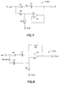
- FIGs. 7, 8 and 9 embodiments are shown of circuitry for using a 2 nd order low pass filter in the AGC block 7'.
- the use of the 2 nd order lowpass filter means that the AC value of the incoming error signal is reduced by a greater amount than would be possible using the conventional 1 st order low pass filter, and thus overcomes the problem that can occur when a previous burst is much stronger (for example 20dB) than the current burst.
- the implementation of the second order low pass filter can be achieved with relatively simple additional components as compared to the prior art circuit.
- Figs. 8 and 9 represent inverting and non-inverting AGC circuit 7' topologies, respectively.
- Figs. 8 and 9 represent inverting and non-inverting AGC circuit 7' topologies, respectively.
- In the inverting AGC circuit topology of Fig. 8 only three components (R 2 , C 2 and a switch DCcomp) are added.
- switch DCcomp When switch DCcomp is open the 2 nd order low pas filter is effectively disabled, as C2 is disconnected from the circuit.
- the state of the switch DCcomp can be controlled by the DSP 180, or with some other logic. Since the size of the resistor R 2 does not degrade the noise performance, it can be made a high value resistance such that the capacitor C 2 can be easily fabricated within an integrated circuit, thereby eliminating the need to provide a separate, discrete capacitor for C2.
- the additional components are R2, R3, R4, R5, C2, amplifier 7B, and switches DCcomp_A, DCcomp_B and XDCcomp, connected as shown.
- switches DCcomp_A, DCcomp_B are opened, and XDCcomp is closed, the circuit is all-pass, i.e., no filtering is performed. This is the normal mode of operation when a signal is received.
- switch DCcomp_A is open, switch DCcomp_B is closed and XDCcomp is open, the circuit is placed into a first order, low pass filter DC compensation mode of operation. This is the conventional DC compensation mode, where the signal across C1 is low pass filtered with a first order filter.
- the circuit of Fig. 9 has only two additional components as compared to the conventional first order low pass filter, i.e., capacitor C2 and switch DCcomp_A.
- switch DCcomp_B is closed (switch DCcomp_B can be controlled by the DSP 180 or by other suitable logic).
- switch DCcomp_B is opened, causing the positive input to operational amplifier 7A to float.
- the gain of operational amplifier 7B, set by R4 and R5, is typically -1.
- operational amplifier 7B effectively inverts the output voltage from operational amplifier 7A.
- the entire circuit may be viewed as operating in a manner that is analogous to a voltage regulator when the DC compensation mode is on, as the DC voltage Vref is forced to appear at the (-) terminal of C1 (with this operational amplifier configuration).
- the level of Vref (e.g., 1.5 VDC) is the DC level that appears at the output of the circuit (node Vout) when the DC compensation mode ends and normal signal reception begins.
- the operational amplifier 7B When the DC compensation is turned off (switches DCcomp_A and DCcomp_B are opened, and XDCcomp is closed) the operational amplifier 7B may be turned off or powered down, as it is not required during the normal signal reception mode of operation.
- the gain of the circuit at this time is simply (1+(R3/R2)).
- An additional advantage made possible by these embodiments is that the operational amplifier(s) that charge the capacitor C1 are not required to deliver large high frequency currents, since at high frequencies the signal is the same on both sides of the capacitor C1. This simplifies the design of the operational amplifiers, and also decreases coupling to the other parts of the integrated circuit via the supply voltages.
- the improved base band section 1B includes the AGC block 7' that contains the AC coupling capacitance C1 coupled in series with the first resistance R1 between the input node of the AGC block 7'and an input to the gain element.
- This method has steps of (A) operating the AC coupling capacitance and the first resistance as a first order low pass filter for attenuating the AC value of an input signal, and (B) closing at least one switch for switching in additional capacitance (C2) and resistance (R2) for transforming the first order low pass filter to a second order low pass filter for increasing the attenuation of the AC value of the input signal.
- an aspect of this invention provides the RF receiver 220 having the RF front end 1A followed by the improved base band section 1B, where the improved base band section 1B includes the AGC block 7' having the DC blocking capacitor (C1) coupled in series between an input node (Vin) of the AGC block and an input to a gain element, in this case the operational amplifier 7A.
- the improved base band section 1B further includes a switch for selectively shorting around the DC blocking capacitor.
- other components may or may not be coupled in series with C1 between Vin and the op-amp 7A, and other components may or may not be coupled around C1.
- the resistor R1 could be placed before or after C1.
- Fig. 12 shows a schematic diagram of an automatic gain control circuit (AGC) in DC-compensation.
- AGC automatic gain control circuit
- the non-inverting input of the operational amplifier 12B is charged to a reference voltage (Vref).
- Vref reference voltage
- the capacitor C1 acts as a DC block.
- Resistors R4 and R5 serve as a voltage divider for operational amplifier 12B.
- Resistor R3 serves as a biasing resistor or a feedback resistor for the inverting input of operational amplifier 12A.
- the DC level may be controlled by modifying Vref.
- Vout can be adjusted to conform to the input of a next stage, which may be, for example, an analog to digital converter (AD-converter), without a DC shifting stage.
- AD-converter analog to digital converter
- the input DC voltage of the operational amplifier is Vref, which facilitates the design of the operational amplifier.
- switches as shown in Fig. 9, may be employed in the AGC circuit of Fig. 12 to control electrical current through the circuit shown in Fig. 12.
- Fig. 13 shows a schematic diagram of an automatic gain control circuit (AGC) that is operational when the charging operational amplifier, shown as 12B in Figure 12, is shut “OFF". As shown in Figure 13, only one operational amplifier 13A is needed to maintain the DC output and to perform the amplification. Resistors R2 and R3 as well as blocking capacitor C1 are also shown.
- AGC automatic gain control circuit
Landscapes
- Engineering & Computer Science (AREA)
- Computer Networks & Wireless Communication (AREA)
- Signal Processing (AREA)
- Circuits Of Receivers In General (AREA)
Abstract
Description
Claims (18)
- A radio frequency RF receiver having an RF front end followed by a base band section, said base band section comprising an automatic gain control AGC block that comprises a DC blocking capacitor coupled in series between an input node of said AGC block and an input to a gain element, said base band section further comprising a switch for selectively shorting around said DC blocking capacitor.
- A receiver as in claim 1, wherein said switch is closed by a mobile station control unit when tuning to another RF channel to make a signal strength measurement.
- A receiver as in claim 1, wherein said switch is closed by a mobile station control unit when resetting said capacitor to a known state.
- A receiver as in claim 1, wherein said gain element is comprised of an operational amplifier connected in an inverting configuration.
- A receiver as in claim 1, wherein said gain element is comprised of an operational amplifier connected in a non-inverting configuration.
- A receiver as in claim 1, wherein said RF front end comprises a direct conversion receiver.
- A radio frequency RF receiver having an RF front end followed by a base band section, said base band section comprising an automatic gain control AGC block that comprises an AC coupling capacitance coupled in series with a first resistance between an input node of said AGC block and an input to a gain element, said AC coupling capacitance and first resistance comprising a first order low pass filter for attenuating the AC value of an input signal appearing across said AC coupling capacitance; said base band section further comprising at least one switch and a capacitance for selectively transforming, when said at least one switch is closed, said first order low pass filter to a second order low pass filter for increasing the attenuation of the AC value of the input signal.
- A receiver as in claim 7, wherein said at least one switch is closed by a mobile station control unit.
- A receiver as in claim 7, wherein said gain element is comprised of an operational amplifier connected in an inverting configuration, wherein said AC coupling capacitance is coupled between an inverting terminal of said operational amplifier and said first resistance, and wherein a second resistance is coupled between a non-inverting input of said operational amplifier and a reference voltage, and said at least one switch and said second capacitance are coupled in series between said input node and said non-inverting terminal of said operational amplifier.
- A receiver as in claim 7, wherein said gain element is comprised of an operational amplifier connected in a non-inverting configuration, wherein said AC coupling capacitance is coupled between a non-inverting terminal of said operational amplifier and said first resistance, wherein a second resistance is coupled between an inverting input of said operational amplifier and a reference voltage, where said at least one switch comprises a first switch, where said first switch and said second capacitance are coupled in series between said input node and said inverting terminal of said operational amplifier, further comprising a second switch and a third resistance coupled in series between said inverting terminal of said operational amplifier and an output terminal of said operational amplifier, and further comprising a second gain element coupled between said output terminal of said operation amplifier and said non-inverting input node of said operational amplifier through a third switch.
- A receiver as claim 10, wherein said second gain element is comprised of a second operational amplifier connected in an inverting configuration with an inverting input coupled to said output terminal of said operational amplifier, an non-inverting terminal coupled to said reference voltage, and an output terminal coupled through said third switch to said non-inverting terminal of said operational amplifier.
- A receiver as in claim 7, wherein said RF front end comprises a direct conversion receiver.
- A method for operating a mobile station that comprises a radio frequency RF receiver having an RF front end followed by a base band section, said base band section comprising an automatic gain control AGC block that comprises a DC blocking capacitor coupled in series between an input node of said AGC block and an input to a gain element, comprising:tuning from a current RF channel to another RF channel to make a signal strength measurement; andreducing a time constant of said AGC circuit by shorting around said DC blocking capacitor.
- A method for operating a mobile station that comprises a radio frequency RF receiver having an RF front end followed by a base band section, said base band section comprising an automatic gain control AGC block that comprises an AC coupling capacitance coupled in series with a first resistance between an input node of said AGC block and an input to a gain element, comprising:operating said AC coupling capacitance and said first resistance as a first order low pass filter for attenuating the AC value of an input signal; andclosing at least one switch for switching in additional capacitance and resistance for transforming said first order low pass filter to a second order low pass filter for increasing the attenuation of the AC value of the input signal.
- A mobile station that includes a radio frequency RF receiver having an RF front end with an output coupled to an input of a base band section, said base band section comprising an automatic gain control AGC block that comprises a capacitance coupled between an input node of said AGC block and an input to a gain element, said AGC block comprising a plurality of switches controlled by a control unit of said mobile station for operating said AGC block in an all-pass signal reception made of operation, or in a first DC compensation mode of operation, where a signal appearing across said capacitance is low pass filtered with a first order filter, or in a second DC compensation mode of operation, where a signal appearing across said capacitance is low pass filtered with a second order filter.
- A radio frequency RF receiver having an RF front end followed by a base band section, said base band section comprising an automatic gain control circuit that comprises an AC coupling capacitance coupled in series with a first resistance between an input node of said automatic gain control circuit and an input to a gain element, said AC coupling capacitance and first resistance comprising a first order low pass filter for attenuating the AC value of an input signal appearing across said AC coupling capacitance; said base band section further comprising a charging operational amplifier of the automatic gain control circuit that enters an OFF state at a predetermined time.
- The receiver as in claim 16, wherein the predetermined time is a reception cycle.
- The receiver as in claim 16, wherein an output from the automatic gain control circuit is modified as a function of a reference potential.
Applications Claiming Priority (2)
| Application Number | Priority Date | Filing Date | Title |
|---|---|---|---|
| US10/054,568 US6975845B2 (en) | 2002-01-22 | 2002-01-22 | Direct conversion receiver architecture |
| US54568 | 2002-01-22 |
Publications (3)
| Publication Number | Publication Date |
|---|---|
| EP1330023A2 true EP1330023A2 (en) | 2003-07-23 |
| EP1330023A3 EP1330023A3 (en) | 2005-05-18 |
| EP1330023B1 EP1330023B1 (en) | 2009-11-25 |
Family
ID=21991999
Family Applications (1)
| Application Number | Title | Priority Date | Filing Date |
|---|---|---|---|
| EP03250300A Expired - Lifetime EP1330023B1 (en) | 2002-01-22 | 2003-01-17 | Direct conversion receiver architecture |
Country Status (3)
| Country | Link |
|---|---|
| US (1) | US6975845B2 (en) |
| EP (1) | EP1330023B1 (en) |
| DE (1) | DE60330203D1 (en) |
Cited By (1)
| Publication number | Priority date | Publication date | Assignee | Title |
|---|---|---|---|---|
| EP2897297A1 (en) * | 2014-01-15 | 2015-07-22 | Climax Technology Co., Ltd | RF module and wireless communication device |
Families Citing this family (8)
| Publication number | Priority date | Publication date | Assignee | Title |
|---|---|---|---|---|
| GB2402008B (en) * | 2003-04-30 | 2006-09-06 | Synad Technologies Ltd | Method and apparatus for DC offset control |
| JP4730153B2 (en) * | 2006-03-15 | 2011-07-20 | 株式会社デンソー | Filter circuit |
| US8195096B2 (en) * | 2006-07-13 | 2012-06-05 | Mediatek Inc. | Apparatus and method for enhancing DC offset correction speed of a radio device |
| IL180673A0 (en) * | 2007-01-11 | 2007-12-03 | Vadim Leibman | Low power radio frequency receiver |
| TWI427984B (en) | 2010-07-20 | 2014-02-21 | 財團法人工業技術研究院 | Current analog analog frequency device |
| US8768277B1 (en) * | 2012-12-19 | 2014-07-01 | Em Microelectronics-Marin S.A. | Automatic gain control of a receiver circuit |
| US9300297B2 (en) | 2013-11-05 | 2016-03-29 | Qualcomm Incorporated | Reference-voltage-less pseudo-differential input circuitry |
| US9491008B2 (en) * | 2014-07-11 | 2016-11-08 | Rambus Inc. | On-chip AC coupled receiver with real-time linear baseline-wander compensation |
Family Cites Families (8)
| Publication number | Priority date | Publication date | Assignee | Title |
|---|---|---|---|---|
| JPS57186815A (en) * | 1981-05-13 | 1982-11-17 | Mitsubishi Electric Corp | Amplitude modulation radio receiver |
| JPS6150354U (en) * | 1984-09-03 | 1986-04-04 | ||
| US5138277A (en) * | 1990-09-28 | 1992-08-11 | Hazeltine Corp. | Signal processing system having a very long time constant |
| US5212826A (en) * | 1990-12-20 | 1993-05-18 | Motorola, Inc. | Apparatus and method of dc offset correction for a receiver |
| DE4135644C1 (en) * | 1991-10-29 | 1993-03-04 | Sgs-Thomson Microelectronics Gmbh, 8011 Grasbrunn, De | |
| FI106328B (en) * | 1996-02-08 | 2001-01-15 | Nokia Mobile Phones Ltd | Method and circuitry for processing a received signal |
| US5930693A (en) * | 1997-02-03 | 1999-07-27 | Ford Motor Company | Radio receiver with underpass detector |
| US6628932B1 (en) * | 2000-09-29 | 2003-09-30 | Northrop Grumman Corporation | Radio receiver automatic gain control techniques |
-
2002
- 2002-01-22 US US10/054,568 patent/US6975845B2/en not_active Expired - Lifetime
-
2003
- 2003-01-17 DE DE60330203T patent/DE60330203D1/en not_active Expired - Lifetime
- 2003-01-17 EP EP03250300A patent/EP1330023B1/en not_active Expired - Lifetime
Cited By (1)
| Publication number | Priority date | Publication date | Assignee | Title |
|---|---|---|---|---|
| EP2897297A1 (en) * | 2014-01-15 | 2015-07-22 | Climax Technology Co., Ltd | RF module and wireless communication device |
Also Published As
| Publication number | Publication date |
|---|---|
| EP1330023A3 (en) | 2005-05-18 |
| DE60330203D1 (en) | 2010-01-07 |
| EP1330023B1 (en) | 2009-11-25 |
| US20030139166A1 (en) | 2003-07-24 |
| US6975845B2 (en) | 2005-12-13 |
Similar Documents
| Publication | Publication Date | Title |
|---|---|---|
| EP1722484B1 (en) | Mobile communication apparatus | |
| US7376400B2 (en) | System and method for digital radio receiver | |
| US7020449B2 (en) | Fast settling variable gain amplifier with DC offset cancellation | |
| US20040142674A1 (en) | Direct conversion receiver having a low pass pole implemented with an active low pass filter | |
| EP1083668A1 (en) | Radio terminal unit | |
| KR20080058437A (en) | Variable gain frequency multiplier | |
| EP1869855B1 (en) | Dc offset correction system for a receiver with baseband gain control | |
| US6144243A (en) | Method and circuit arrangement for reducing offset voltage of a signal | |
| EP1486012A1 (en) | Method and apparatus providing calibration technique for rf performance tuning | |
| US11159146B2 (en) | Reconfigurable analog filter and integrated circuit including the same | |
| US6853235B2 (en) | High frequency switch, amplifying circuit, and mobile communication terminal | |
| EP1330023B1 (en) | Direct conversion receiver architecture | |
| WO2004004146A1 (en) | Offset compensation in a direct-conversion receiver | |
| US6324230B1 (en) | Multimode fast attack automatic gain control (AGC) loop for narrow band receivers | |
| EP3146628B1 (en) | Differential mode bandwidth extension technique with common mode compensation | |
| US6591093B1 (en) | Circuit and method for frequency translation | |
| US20080026719A1 (en) | Apparatus and method for enhancing dc offset correction speed of a radio device | |
| US7454186B2 (en) | Direct conversion receiving apparatus and celluar phone | |
| US7493097B2 (en) | High dynamic range compact mixer output stage for a wireless receiver | |
| JP2001016121A (en) | Filter device and wireless receiving device | |
| JP2000286746A (en) | Mobile communication device | |
| JP2001044775A (en) | Gain control circuit | |
| GB2376823A (en) | A radio transmitter comprising power amplifier circuitry wherein a filter is adjusted based on input power level or mode of the transmitter |
Legal Events
| Date | Code | Title | Description |
|---|---|---|---|
| PUAI | Public reference made under article 153(3) epc to a published international application that has entered the european phase |
Free format text: ORIGINAL CODE: 0009012 |
|
| AK | Designated contracting states |
Designated state(s): AT BE BG CH CY CZ DE DK EE ES FI FR GB GR HU IE IT LI LU MC NL PT SE SI SK TR |
|
| AX | Request for extension of the european patent |
Extension state: AL LT LV MK RO |
|
| PUAL | Search report despatched |
Free format text: ORIGINAL CODE: 0009013 |
|
| AK | Designated contracting states |
Kind code of ref document: A3 Designated state(s): AT BE BG CH CY CZ DE DK EE ES FI FR GB GR HU IE IT LI LU MC NL PT SE SI SK TR |
|
| AX | Request for extension of the european patent |
Extension state: AL LT LV MK RO |
|
| 17P | Request for examination filed |
Effective date: 20050921 |
|
| AKX | Designation fees paid |
Designated state(s): DE FI FR GB NL |
|
| 17Q | First examination report despatched |
Effective date: 20060209 |
|
| GRAP | Despatch of communication of intention to grant a patent |
Free format text: ORIGINAL CODE: EPIDOSNIGR1 |
|
| GRAS | Grant fee paid |
Free format text: ORIGINAL CODE: EPIDOSNIGR3 |
|
| GRAJ | Information related to disapproval of communication of intention to grant by the applicant or resumption of examination proceedings by the epo deleted |
Free format text: ORIGINAL CODE: EPIDOSDIGR1 |
|
| GRAP | Despatch of communication of intention to grant a patent |
Free format text: ORIGINAL CODE: EPIDOSNIGR1 |
|
| GRAS | Grant fee paid |
Free format text: ORIGINAL CODE: EPIDOSNIGR3 |
|
| GRAA | (expected) grant |
Free format text: ORIGINAL CODE: 0009210 |
|
| AK | Designated contracting states |
Kind code of ref document: B1 Designated state(s): DE FI FR GB NL |
|
| REG | Reference to a national code |
Ref country code: GB Ref legal event code: FG4D |
|
| REF | Corresponds to: |
Ref document number: 60330203 Country of ref document: DE Date of ref document: 20100107 Kind code of ref document: P |
|
| REG | Reference to a national code |
Ref country code: NL Ref legal event code: VDEP Effective date: 20091125 |
|
| PG25 | Lapsed in a contracting state [announced via postgrant information from national office to epo] |
Ref country code: FI Free format text: LAPSE BECAUSE OF FAILURE TO SUBMIT A TRANSLATION OF THE DESCRIPTION OR TO PAY THE FEE WITHIN THE PRESCRIBED TIME-LIMIT Effective date: 20091125 |
|
| PG25 | Lapsed in a contracting state [announced via postgrant information from national office to epo] |
Ref country code: NL Free format text: LAPSE BECAUSE OF FAILURE TO SUBMIT A TRANSLATION OF THE DESCRIPTION OR TO PAY THE FEE WITHIN THE PRESCRIBED TIME-LIMIT Effective date: 20091125 |
|
| PLBE | No opposition filed within time limit |
Free format text: ORIGINAL CODE: 0009261 |
|
| STAA | Information on the status of an ep patent application or granted ep patent |
Free format text: STATUS: NO OPPOSITION FILED WITHIN TIME LIMIT |
|
| REG | Reference to a national code |
Ref country code: FR Ref legal event code: ST Effective date: 20100930 |
|
| PG25 | Lapsed in a contracting state [announced via postgrant information from national office to epo] |
Ref country code: FR Free format text: LAPSE BECAUSE OF NON-PAYMENT OF DUE FEES Effective date: 20100201 |
|
| 26N | No opposition filed |
Effective date: 20100826 |
|
| REG | Reference to a national code |
Ref country code: GB Ref legal event code: 732E Free format text: REGISTERED BETWEEN 20150910 AND 20150916 |
|
| REG | Reference to a national code |
Ref country code: DE Ref legal event code: R081 Ref document number: 60330203 Country of ref document: DE Owner name: NOKIA TECHNOLOGIES OY, FI Free format text: FORMER OWNER: NOKIA CORP., 02610 ESPOO, FI |
|
| PGFP | Annual fee paid to national office [announced via postgrant information from national office to epo] |
Ref country code: DE Payment date: 20180103 Year of fee payment: 16 Ref country code: GB Payment date: 20180117 Year of fee payment: 16 |
|
| REG | Reference to a national code |
Ref country code: DE Ref legal event code: R119 Ref document number: 60330203 Country of ref document: DE |
|
| GBPC | Gb: european patent ceased through non-payment of renewal fee |
Effective date: 20190117 |
|
| PG25 | Lapsed in a contracting state [announced via postgrant information from national office to epo] |
Ref country code: DE Free format text: LAPSE BECAUSE OF NON-PAYMENT OF DUE FEES Effective date: 20190801 |
|
| PG25 | Lapsed in a contracting state [announced via postgrant information from national office to epo] |
Ref country code: GB Free format text: LAPSE BECAUSE OF NON-PAYMENT OF DUE FEES Effective date: 20190117 |