EP1328012A1 - Method of manufactoring an electronic device comprising an inductive mirco component - Google Patents
Method of manufactoring an electronic device comprising an inductive mirco component Download PDFInfo
- Publication number
- EP1328012A1 EP1328012A1 EP02356230A EP02356230A EP1328012A1 EP 1328012 A1 EP1328012 A1 EP 1328012A1 EP 02356230 A EP02356230 A EP 02356230A EP 02356230 A EP02356230 A EP 02356230A EP 1328012 A1 EP1328012 A1 EP 1328012A1
- Authority
- EP
- European Patent Office
- Prior art keywords
- copper
- layer
- substrate
- depositing
- turns
- Prior art date
- Legal status (The legal status is an assumption and is not a legal conclusion. Google has not performed a legal analysis and makes no representation as to the accuracy of the status listed.)
- Withdrawn
Links
Images

Classifications
-
- H—ELECTRICITY
- H01—ELECTRIC ELEMENTS
- H01L—SEMICONDUCTOR DEVICES NOT COVERED BY CLASS H10
- H01L28/00—Passive two-terminal components without a potential-jump or surface barrier for integrated circuits; Details thereof; Multistep manufacturing processes therefor
- H01L28/10—Inductors
-
- H—ELECTRICITY
- H01—ELECTRIC ELEMENTS
- H01L—SEMICONDUCTOR DEVICES NOT COVERED BY CLASS H10
- H01L27/00—Devices consisting of a plurality of semiconductor or other solid-state components formed in or on a common substrate
- H01L27/02—Devices consisting of a plurality of semiconductor or other solid-state components formed in or on a common substrate including semiconductor components specially adapted for rectifying, oscillating, amplifying or switching and having at least one potential-jump barrier or surface barrier; including integrated passive circuit elements with at least one potential-jump barrier or surface barrier
- H01L27/04—Devices consisting of a plurality of semiconductor or other solid-state components formed in or on a common substrate including semiconductor components specially adapted for rectifying, oscillating, amplifying or switching and having at least one potential-jump barrier or surface barrier; including integrated passive circuit elements with at least one potential-jump barrier or surface barrier the substrate being a semiconductor body
- H01L27/08—Devices consisting of a plurality of semiconductor or other solid-state components formed in or on a common substrate including semiconductor components specially adapted for rectifying, oscillating, amplifying or switching and having at least one potential-jump barrier or surface barrier; including integrated passive circuit elements with at least one potential-jump barrier or surface barrier the substrate being a semiconductor body including only semiconductor components of a single kind
-
- H—ELECTRICITY
- H01—ELECTRIC ELEMENTS
- H01L—SEMICONDUCTOR DEVICES NOT COVERED BY CLASS H10
- H01L21/00—Processes or apparatus adapted for the manufacture or treatment of semiconductor or solid state devices or of parts thereof
- H01L21/02—Manufacture or treatment of semiconductor devices or of parts thereof
- H01L21/04—Manufacture or treatment of semiconductor devices or of parts thereof the devices having at least one potential-jump barrier or surface barrier, e.g. PN junction, depletion layer or carrier concentration layer
- H01L21/18—Manufacture or treatment of semiconductor devices or of parts thereof the devices having at least one potential-jump barrier or surface barrier, e.g. PN junction, depletion layer or carrier concentration layer the devices having semiconductor bodies comprising elements of Group IV of the Periodic System or AIIIBV compounds with or without impurities, e.g. doping materials
- H01L21/28—Manufacture of electrodes on semiconductor bodies using processes or apparatus not provided for in groups H01L21/20 - H01L21/268
- H01L21/283—Deposition of conductive or insulating materials for electrodes conducting electric current
- H01L21/288—Deposition of conductive or insulating materials for electrodes conducting electric current from a liquid, e.g. electrolytic deposition
- H01L21/2885—Deposition of conductive or insulating materials for electrodes conducting electric current from a liquid, e.g. electrolytic deposition using an external electrical current, i.e. electro-deposition
-
- H—ELECTRICITY
- H01—ELECTRIC ELEMENTS
- H01L—SEMICONDUCTOR DEVICES NOT COVERED BY CLASS H10
- H01L21/00—Processes or apparatus adapted for the manufacture or treatment of semiconductor or solid state devices or of parts thereof
- H01L21/70—Manufacture or treatment of devices consisting of a plurality of solid state components formed in or on a common substrate or of parts thereof; Manufacture of integrated circuit devices or of parts thereof
- H01L21/71—Manufacture of specific parts of devices defined in group H01L21/70
- H01L21/768—Applying interconnections to be used for carrying current between separate components within a device comprising conductors and dielectrics
- H01L21/76838—Applying interconnections to be used for carrying current between separate components within a device comprising conductors and dielectrics characterised by the formation and the after-treatment of the conductors
Definitions
- the invention relates to the field of microelectronics. More specifically, it targets a process for making micro-components inductive on a substrate, which can itself incorporate an integrated circuit.
- These components can in particular be used in applications of the type radio frequencies, for example in the telecommunications field.
- the invention relates more specifically to a method for obtaining circuits with significantly higher performance than components existing, particularly with regard to the value of the quality factor.
- the process subject of the invention also limits the number of steps required for the production of such components, and ensures good reproducibility of characteristics of the components it makes it possible to manufacture.
- Such a method has a number of drawbacks, among which are can basically note the fact that the electrolytic deposition step ensures both the formation of the coils of the inductive component, as well as the filling of the hole interconnection, allowing contact with the metal stud connected to the circuit integrated. These zones being of different depths, it follows that the deposit electrolytic is carried out differently at the level of the turns and at the level of the interconnect hole. We thus observe certain irregularities in the formation of the turns which are detrimental to the good regularity of the performances electrical components of the inductive component.
- One of the objectives of the invention is to overcome these various drawbacks, and in particular to make it possible to produce components which have dimensional characteristics as precise as possible, so as to provide optimal electrical performance.
- the invention therefore relates to a method of manufacturing a component electronic.
- a component incorporates an inductive micro-component, such as a inductor or transformer, which is located above a substrate, and connected to it substrate at least by a metal stud.
- an inductive micro-component such as a inductor or transformer
- the method according to the invention follows a number of steps which provide certain improvements over the methods of the prior art.
- the electrolytic deposition of copper occurs in two distinct stages, namely first of all a first stage allowing to fill the interconnection hole, which initially allows the growth of copper up to the level of the lower plane of the inductive micro-component.
- second stage an electrolytic deposition of copper is carried out, which forms simultaneously the turns of the inductive component and the connection area of the turns with the via already filled in the previous deposit step.
- the method can be implemented works on a semiconductor substrate, and in particular a substrate having been previously functionalized to form an integrated circuit.
- it may be a specific substrate, such as than an amorphous substrate of the glass or quartz type, or more generally a substrate having electrical, optical or magnetic properties suitable for some applications.
- the material of low relative permittivity, which is deposited on the substrate can be benzocyclobutene (BCB), or even a material analog, whose relative permittivity is typically less than 3.
- BCB benzocyclobutene
- this layer of low permittivity material can be between 10 and 40 micrometers, preferably being close to 20 micrometers.
- the thickness of this layer substantially defines the distance between the inductive component and the substrate. This distance, combined with the permittivity relative of the material of this layer defines the parasitic capacity existing between the inductive component and the substrate, a capacity which it is highly desirable to minimize.
- the material used to form the hard mask above the BCB can be chosen from the group comprising: SiC, SiOC, SiN, SiON, Si 3 N 4 , SiO 2 , Y 2 O 3 , Cr taken alone or in combination.
- These materials have properties of good compatibility with BCB, in particular a strong adhesion as a hard mask on the surface of the BCB. These materials have adequate mechanical properties for their use in masking, which avoids the appearance of too strong constraints at the level of the junction between the hard mask and the underlying layer of BCB. Furthermore, by a judicious choice of these materials having the function of a hard mask for the purpose of etching of interconnection holes, high selectivity of etching of BCB compared to these materials is acquired, so as to avoid any over-etching of the BCB and thus obtain the desired profiles without delamination.
- a layer forming is deposited barrier to diffusion of copper above the layer of weak material relative permittivity, when the hard mask has been removed.
- This barrier layer allows to isolate the underlying layer of copper which will be later deposited, in particular in the form of the primer layer.
- This barrier layer characteristic prevents migration of copper through the weak layer relative permittivity, which would increase this permittivity, and therefore to increase the parasitic capacitance between the inductive micro-component and the substrate and create sources of defect.
- This barrier layer also prevents the copper does not migrate inside the substrate, with consequences detrimental to the quality or functioning of the integrated circuit.
- the barrier layer can be made of tungsten or from a material chosen from the group comprising TiW, Ti, TiN, Ta, TaN, Mo, WN, Ru, Re, Cr, Os. These materials can be used alone or in combination.
- the diffusion barrier layer may have a thickness between 100 and 400 ⁇ .
- the method can include a enrichment step of the copper primer layer.
- This primer layer plays the role of electrode for subsequent copper deposits by electrolytic means.
- This primer layer is deposited by physico-chemical and more particularly by the so-called spraying technique and according to its variant of ionized metal plasma source.
- a enrichment step of this primer layer by subjecting the primer layer to an electrolyte bath.
- This bath comprising copper salts allows a deposit of copper in any spaces existing between the copper islands beforehand deposited during the production of the primer layer. This enrichment step therefore ensures a smoothing of this primer layer so as to improve the deposition subsequent electrolytic.
- an annealing step can be carried out, allowing the size of the copper crystals deposited during the steps of electrolytic deposition.
- This annealing step typically by exposure of the component at a temperature between 150 and 400 ° C for a period of a few minutes, ensures crystal uniformity of the deposited copper, and therefore the homogeneity and the conductive nature of the copper which will form the turns of the inductive component. This improves the electrical qualities of the component by reducing the number of singularities that can be the source of resistive points or mechanical weaknesses.
- a step of decontamination of copper liable to migrate into the substrate, in particular at level of the lateral and posterior faces of the substrate as well as at its circumference.
- a bath containing copper salts soluble in a judiciously chosen solvent an excess of copper deposit.
- this metal is deposited using techniques electrolysis and according to a specific current distribution between the cathode and the anode, there is generally an excess of copper deposit in the circumference of the substrate.
- the convection and mass transfer process which is the basis of the technique of deposition by electrolysis of the element Copper, generates on the lateral or posterior faces of the substrate possible flow and diffusion over certain areas of the substrate. In order to avoid their possible migration into the substrate it is recommended to use this step.
- this decontamination step can take place after one and the other of the two stages of electroplating.
- the protective mask deposited during the step following the deposit of copper primer layers can be formed from a photonegative resin. This allows its elimination in an easy way at the bottom of the interconnection hole in which the first electrolytic deposition of copper will take place later.
- the modification properties of the photosensitive resin allows it to harden on exposed areas during the exposure of the lithography mask. This prevents copper deposits on the surface, thanks to the screen thus formed on the surface of the enriched primer layer by the hardened resin.
- HMDS hexamethyledisilazane
- DVTMDS divinyltetramethyldisilazane
- certain non-corrosive chemical cleaning steps with respect to copper can take place after the electrolytic deposition of copper, as well as after the step of depositing the copper primer layer, or else the deposition of the copper diffusion barrier layer.
- the invention also relates to an electronic micro-component capable of be carried out according to the process described above.
- a component incorporates a inductive micro-component located on a substrate, and connected to the latter by at least a metal stud.
- the invention relates to a method making it possible to carry out inductive micro-components on a substrate.
- the substrate (1) used is a substrate having previously been treated with so as to form an integrated circuit.
- other different substrates can be used, such as in particular substrates based on quartz or glass.
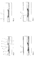
- such a substrate (1) as illustrated in FIG. 1, comprises the level upper (2) of the integrated circuit proper, surmounted by a layer (3) of doped substrate.
- the substrate (1) also includes a pad metallic (4), made of a metal which can be aluminum or an alloy aluminum or copper, the upper face (5) of which is accessible. Edges (6) of this metal pad, as well as the upper face (7) of the doped layer are covered with a passivation layer (8).
- the first step consists in ensuring a cleaning of the upper face (5) of the metallic connection pad (4) as well as the passivation layer (8) deposited on the substrate. This cleaning is carried out by wet chemical means.
- a layer is subsequently deposited (10) benzocyclobutene (BCB), or a possible equivalent material, having a relative permittivity of less than 3.
- This deposition is carried out by a process known as “spin deposit”, also called “Spin on deposition”.
- spin deposit also called “Spin on deposition”.
- the thickness deposited is close to 20 micrometers.
- a layer (12) forming a hard mask is then deposited on top of the BCB layer (10).
- This layer (12) has a thickness of the order of 200 ⁇ .
- the material used is preferably silicon carbide (SiC), but it could also be SiOC, SiN, Si 3 N 4 , SiON, SiO 4 , SiO 2 , Cr or Y 2 O 3 or any other material, since the etching selectivity with respect to the material of the lower layer is at least 10: 1.
- This layer (12) of hard mask can be deposited by a chemical vapor deposition process assisted by plasma, or PECVD for "Plasma Enhanced Chemical Vapor Deposition".
- an opening (13) is made in the hard mask (12), as illustrated in FIG. 4, by a lithography process and an appropriate chemical etching using a wet process such as a bath based on hypophosphoric acid at a temperature of 180 ° C., if the hard mask is composed of silicon nitride, or a dry etching by plasma using a reactive gas comprising fluorine such as CF 4 : H 2 for example.
- the etching of the BCB layer can be carried out in particular by the use of a gas mixture such as the Ar / CF 4 / O 2 mixture or even by a radiofrequency plasma using other reactants.
- the hard mask which remains on the remaining parts of the BCB layer (10) is removed.
- This hard mask is removed by pickling, using a solution composed of Ce (SO4) 2 ; 2 (NH4) 2 SO 4 : HClO 4 : Deionized water if the hard mask is in chromium for example.
- the hard mask may also not be eliminated, and therefore stored on the layer (10) of BCB, depending on the material which constitutes it, and in particular if it is SiC, SiN or SiON for example.
- a layer is subsequently deposited (15) barrier to copper diffusion.
- This layer (15) is preferably made of in an alloy of Titanium and Tungsten, or in a superposition of Titanium and Titanium nitride, or even tantalum and tantalum nitride.
- This layer (15) can also be made of Tungsten Nitride, or else by a simple layer of Tungsten, Molybdenum, Osmium, or Ruthenium.
- This layer (15), with a thickness between 100 and 400 ⁇ , can be deposited by different techniques, and in particular by spraying, a process also known as the abbreviation for PVD - IMP for "Physical Vapor Deposition - Ionized Metal Plasma ", or by chemical vapor deposition techniques known as name of CVD “Chemical Vapor Deposition” and ALD “Atomic Layer Deposition ”.
- a layer is subsequently deposited (16) copper primer.
- This primer layer (16) can be deposited by different techniques, and in particular by spraying, a process also known as the abbreviation for PVD - IMP for "Physical Vapor Deposition - Ionized Metal Plasma ", or by chemical vapor deposition techniques known as name of CVD “Chemical Vapor Deposition” and ALD “Atomic Layer Deposition The layer thus obtained has a thickness typically between 500 and 2000 ⁇ .
- a step of enriching the primer layer (16) is carried out by electrolytic means.
- electrolytic means One can use a bath of copper salts, such as CuSO 4 : 5H 2 O.
- a reducing agent such as dimethylamineborane, in substitution for the electrolytic current.
- This enrichment step makes it possible to fill the spaces between the islands of copper which have been previously deposited to form the primer layer.
- the surface the primer layer (16) is thus smoothed, which favors the subsequent step of electrolytic deposition.
- This step increases the thickness of the layer primer inside the via and more particularly on the interior faces and bottom of the interconnecting hole.
- a cleaning step is carried out by applying a non-corrosive solution for copper, so as to obtain a surface finish optimal with regard to the bottom (19) of the interconnection hole as well as its side walls (21).
- the bath used is an aqueous solution and may contain corrosion inhibiting molecules such as benzotriazole.
- a deposit copper electrolytic so as to fill the hole (22) interconnection (14) by a technique known as "electroplating".
- This technique is based on the use of an electrolyte bath, the formulation is judiciously defined to obtain a quality of Copper optimal, i.e. resistivity before grain growth during annealing between 1.9 ⁇ .cm and 2.3 ⁇ .cm and preferably between 2 ⁇ .cm and 2.15 ⁇ .cm.
- the definition of deposit is directly dependent on the geometry of the electrochemical cell, the distance between the cathode and the anode, the shape and characteristics of each electrode as well as the area and the surface on which we are going to deposit.
- the baths used can be for example those marketed under the name "Cu VIAFORM" by the company ENTHONE, or "Cu GLEAM ELECTRODEPOSIT 6000" by the company SHIPLEY.
- This decontamination step notably makes it possible to clean the back of the substrate, as well as the peripheral areas of the substrate. Among these peripheral areas, hear the lateral faces of the substrate, perpendicular to the main plane of the substrate as well as the edges of the substrate on which deposits may have accumulated copper superfluous linked to the copper deposition process according to the technique used.
- tool means allowing the face-to-face treatment of the substrate, using a bath containing a mixture of hydrogen peroxide and sulfuric acid.
- a cleaning step is then carried out by applying a bath. non-corrosive to copper, so as to eliminate all traces of resin on the primer layer (10), in order to facilitate the deposition of the subsequent layers.
- annealing allowing to reorganize the crystal structure of the copper (22) deposited in the interconnection hole (14), increasing the size of the elementary crystalline grains.
- This step uses a technique known as “RTP” for "Rapid Thermal Processing” during which the component is subjected to a temperature of the order of 150 to 400 ° C, preferably around 300 ° C, for a period of 10 seconds to 30 minutes and preferably for 5 minutes.
- the component is kept under an atmosphere of an inert gas or under vacuum avoiding any oxidation and diffusion of oxygen in the crystal medium of copper.
- the definition of parameters is judiciously chosen to obtain an optimal quality of Copper namely a resistivity after growth of the grains of between 1.7 ⁇ .cm and 2 ⁇ .cm but preferably between 1.72 ⁇ .cm and 1.82 ⁇ .cm.
- HMDS hexamethyledisilazane
- DVTMDS divinyltetramethyldisilazane
- This resin (25) is of the positive photosensitive type, to allow subsequent lithographies. This resin (25) resists chemistry acids from electrolytic deposits.
- the upper resin layer (25) thus deposited has a thickness between 10 and 50 microns, preferably between 20 and 40 microns, depending on the height of the turns of the inductive component.
- a deposit is made. copper electrolytic, above the primer layer (16). Note that the thickness deposited in the peripheral channels (28) is the same as that in the channel (29) located directly above the interconnection hole (4), so that the growth is substantially similar.
- the electrolytic deposition of copper can in this case precisely be done by means of an electrochemical deposition tool using a soluble copper anode and a chemical bath chosen from the different producers such as the “Cu gleam electrodeposit 6000” bath marketed by the Shipley company.
- the copper deposit typically fills between 70% and 90% of channels (29), so as to give copper thicknesses for the turns larger than 10 micrometers.
- step # 16 Thereafter, a decontamination step identical to that is carried out. described in step # 16.
- step No. 18 we proceed as already mentioned in step No. 18 to a step of cleaning by applying a non-corrosive copper bath to remove all the residues generated by the lithography step, the chemical process of which can use a compound of amines and anti-corrosion molecules of the chosen copper among the manufacturers of such products as the company's product ACT-970 Ashland.
- anisotropic of the copper primer layer (16) for example by means of a bath sulfuric acid, or a nitric acid bath including benzotriazole.
- the engraving of the layer (15) barrier to the diffusion of copper which is dependent on the choice of copper diffusion barrier material.
- this diffusion barrier can be etched with an aqueous solution composed of ethylene diamine tetra acetic acid (EDTA) and peroxide of hydrogen in a ratio of 2 to 1, at a temperature between 45 ° C and 90 ° C and preferably around 65 ° C.
- EDTA ethylene diamine tetra acetic acid
- peroxide of hydrogen in a ratio of 2 to 1, at a temperature between 45 ° C and 90 ° C and preferably around 65 ° C.
- this example is not limiting and other chemical baths can be used according to the state of the art.
- a cleaning step is carried out using a non-corrosive bath. for copper as analogous to that described in steps 18 and 26.
- the process according to the invention allows to obtain inductive micro-components which have a very high factor of quality, due to a controlled distance between the substrate and the main plane of the inductive micro-component.
- the quality factors obtained are greater than 40, at frequencies of the order of 2 GigaHertz.
- Decomposition of the electrolytic deposit of copper in two distinct stages allows to optimize the regularity of the shape of the different turns without increasing the manufacturing cost, and thus therefore good reproducibility of the process leading to the production of micro-component having electrical characteristics very close to those defined during design and therefore expected electrical performance.
- the advantage of this present invention is to control the interfaces between the different layers of materials deposited and formed which has as a consequence a marked improvement in the performance of the device and a marked reduction in sources of defect.
Abstract
Description
L'invention se rattache au domaine de la microélectronique. Plus précisément, elle vise un procédé permettant de réaliser des micro-composants inductifs sur un substrat, qui peut lui-même incorporer un circuit intégré.The invention relates to the field of microelectronics. More specifically, it targets a process for making micro-components inductive on a substrate, which can itself incorporate an integrated circuit.
Ces composants peuvent notamment être utilisés dans les applications de type radiofréquences, par exemple dans le domaine des télécommunications.These components can in particular be used in applications of the type radio frequencies, for example in the telecommunications field.
L'invention vise plus spécifiquement un procédé permettant d'obtenir des circuits possédant des performances nettement plus élevées que les composants existants, notamment en ce qui concerne la valeur du facteur de qualité. Le procédé objet de l'invention, limite également le nombre d'étapes nécessaires pour la réalisation de tels composants, et assure une bonne reproductibilité des caractéristiques des composants qu'il permet de fabriquer.The invention relates more specifically to a method for obtaining circuits with significantly higher performance than components existing, particularly with regard to the value of the quality factor. The process subject of the invention, also limits the number of steps required for the production of such components, and ensures good reproducibility of characteristics of the components it makes it possible to manufacture.
Dans le document FR 2 791 470, le Demandeur a décrit un procédé de
fabrication permettant de réaliser des micro-inductances ou des microtransformateurs
au-dessus d'un substrat, et notamment au-dessus d'un circuit
intégré. De façon résumée, ce procédé consiste à déposer une couche de matériau
de faible permittivité relative puis à réaliser une gravure de ce matériau au niveau
d'une ouverture réalisée dans un masque dur, à l'aplomb d'un plot de connexion
avec le reste du circuit intégré, de manière à définir un trou d'interconnexion,
également appelé "via"In
Après avoir déposé une résine au-dessus du masque dur, on grave cette dernière pour former les canaux définissant la géométrie des spires du composant inductif. On procède par la suite à un dépôt de cuivre, par voie électrolytique, au-dessus du plot de connexion, et dans les canaux définis dans la résine supérieure. After having deposited a resin on top of the hard mask, we engrave this last to form the channels defining the geometry of the turns of the component inductive. Copper is then deposited, electrolytically, on top of the connection pad, and in the channels defined in the upper resin.
Un tel procédé présente un certain nombre d'inconvénients, parmi lesquels on peut noter essentiellement le fait que l'étape de dépôt électrolytique assure à la fois la formation des spires du composant inductif, ainsi que le remplissage du trou d'interconnexion, permettant le contact avec le plot métallique relié au circuit intégré. Ces zones étant de profondeurs différentes, il s'ensuit que le dépôt électrolytique s'effectue de manière différente au niveau des spires et au niveau du trou d'interconnexion. On observe ainsi certaines irrégularités au niveau de la formation des spires qui sont préjudiciables à la bonne régularité des performances électriques du composant inductif.Such a method has a number of drawbacks, among which are can basically note the fact that the electrolytic deposition step ensures both the formation of the coils of the inductive component, as well as the filling of the hole interconnection, allowing contact with the metal stud connected to the circuit integrated. These zones being of different depths, it follows that the deposit electrolytic is carried out differently at the level of the turns and at the level of the interconnect hole. We thus observe certain irregularities in the formation of the turns which are detrimental to the good regularity of the performances electrical components of the inductive component.
En outre, lors de l'étape de gravure de la résine supérieure, il est nécessaire d'effectuer une gravure plus longue au niveau du trou d'interconnexion, par comparaison avec les zones dans lesquelles sont formés les canaux destinés à recevoir les spires. Cette différence de profondeur de gravure provoque une libération de composés chimiques au niveau du fond du trou d'interconnexion, ce qui perturbe l'opération ultérieure de dépôt électrolytique de cuivre.In addition, during the etching step of the upper resin, it is necessary to carry out a longer etching at the level of the interconnection hole, by comparison with the areas in which the channels intended for receive the turns. This difference in engraving depth causes a release of chemical compounds at the bottom of the via hole, this which disrupts the subsequent electrolytic deposition of copper.
Un des objectifs de l'invention est de pallier ces différents inconvénients, et notamment de permettre de réaliser des composants qui possèdent des caractéristiques dimensionnelles aussi précises que possible, de manière à conférer des performances électriques optimales.One of the objectives of the invention is to overcome these various drawbacks, and in particular to make it possible to produce components which have dimensional characteristics as precise as possible, so as to provide optimal electrical performance.
L'invention concerne donc un procédé de fabrication d'un composant électronique. Un tel composant incorpore un micro-composant inductif, tel qu'une inductance ou un transformateur, qui est situé au-dessus d'un substrat, et relié à ce substrat au moins par un plot métallique.The invention therefore relates to a method of manufacturing a component electronic. Such a component incorporates an inductive micro-component, such as a inductor or transformer, which is located above a substrate, and connected to it substrate at least by a metal stud.
Conformément à l'invention, ce procédé se caractérise en ce qu'il comporte
les étapes suivantes :
Ainsi, le procédé conforme à l'invention enchaíne un certain nombre d'étapes qui procurent certaines améliorations par rapport aux procédés de l'Art antérieur. On notera notamment que le dépôt électrolytique de cuivre intervient en deux étapes distinctes, à savoir tout d'abord une première étape permettant de combler le trou d'interconnexion, ce qui permet dans un premier temps de faire croítre du cuivre jusqu'au niveau du plan inférieur du micro-composant inductif. Dans une seconde étape, on procède à un dépôt électrolytique de cuivre, qui forme simultanément les spires du composant inductif et la zone de liaison des spires avec la via déjà comblée dans l'étape de dépôt antérieur. Thus, the method according to the invention follows a number of steps which provide certain improvements over the methods of the prior art. It will be noted in particular that the electrolytic deposition of copper occurs in two distinct stages, namely first of all a first stage allowing to fill the interconnection hole, which initially allows the growth of copper up to the level of the lower plane of the inductive micro-component. In second stage, an electrolytic deposition of copper is carried out, which forms simultaneously the turns of the inductive component and the connection area of the turns with the via already filled in the previous deposit step.
De la sorte, en dissociant ces deux dépôts de cuivre, on assure une homogénéité de ce dépôt qui est favorable à la régularité de la forme des spires, et donc à la qualité des performances électriques ainsi qu'à la reproductibilité du procédé.In this way, by dissociating these two copper deposits, a homogeneity of this deposit which is favorable to the regularity of the shape of the turns, and therefore to the quality of the electrical performances as well as to the reproducibility of the process.
On notera également que ce procédé peut être utilisé sur différents types de substrat. Ainsi, dans une première famille d'application, le procédé peut être mis en oeuvre sur un substrat semi-conducteur, et notamment un substrat ayant été préalablement fonctionnalisé pour former un circuit intégré.It should also be noted that this process can be used on different types of substrate. Thus, in a first family of applications, the method can be implemented works on a semiconductor substrate, and in particular a substrate having been previously functionalized to form an integrated circuit.
Dans d'autres types d'applications, il peut s'agir d'un substrat spécifique, tel qu'un substrat amorphe du type verre ou quartz, ou plus généralement un substrat possédant des propriétés électriques, optiques ou magnétiques appropriées à certaines applications.In other types of applications, it may be a specific substrate, such as than an amorphous substrate of the glass or quartz type, or more generally a substrate having electrical, optical or magnetic properties suitable for some applications.
En pratique, le matériau de faible permittivité relative, qui est déposé sur le substrat peut être du benzocyclobutène (BCB), ou voire encore un matériau analogue, dont la permittivité relative est typiquement inférieure à 3.In practice, the material of low relative permittivity, which is deposited on the substrate can be benzocyclobutene (BCB), or even a material analog, whose relative permittivity is typically less than 3.
En pratique, l'épaisseur de cette couche de matériau de faible permittivité relative peut être comprise entre 10 et 40 micromètres, étant préférentiellement voisine de 20 micromètres.In practice, the thickness of this layer of low permittivity material relative can be between 10 and 40 micrometers, preferably being close to 20 micrometers.
L'épaisseur de cette couche définit sensiblement l'éloignement entre le composant inductif et le substrat. Cette distance, combinée avec la permittivité relative du matériau de cette couche définit la capacité parasite existant entre le composant inductif et le substrat, capacité qu'il est hautement souhaitable de minimiser.The thickness of this layer substantially defines the distance between the inductive component and the substrate. This distance, combined with the permittivity relative of the material of this layer defines the parasitic capacity existing between the inductive component and the substrate, a capacity which it is highly desirable to minimize.
En pratique, le matériau utilisé pour former le masque dur au-dessus du BCB peut être choisi dans le groupe comprenant : SiC, SiOC, SiN, SiON, Si3N4, SiO2, Y2O3, Cr pris isolément ou en combinaison. In practice, the material used to form the hard mask above the BCB can be chosen from the group comprising: SiC, SiOC, SiN, SiON, Si 3 N 4 , SiO 2 , Y 2 O 3 , Cr taken alone or in combination.
Ces matériaux présentent des propriétés de bonne compatibilité avec le BCB, notamment une forte adhésion comme masque dur sur la surface du BCB. Ces matériaux présentent des propriétés mécaniques adéquates pour leur utilisation en masquinage, ce qui évite l'apparition de trop fortes contraintes au niveau de la jonction entre le masque dur et la couche sous-jacente de BCB. Par ailleurs, par un choix judicieux de ces matériaux ayant pour fonction de masque dur à des fins de gravure des trous d'interconnexion, une sélectivité élevée de la gravure du BCB par rapport à ces matériaux est acquise, de manière à éviter toute sur-gravure du BCB et obtenir ainsi les profiles souhaités sans délaminage.These materials have properties of good compatibility with BCB, in particular a strong adhesion as a hard mask on the surface of the BCB. These materials have adequate mechanical properties for their use in masking, which avoids the appearance of too strong constraints at the level of the junction between the hard mask and the underlying layer of BCB. Furthermore, by a judicious choice of these materials having the function of a hard mask for the purpose of etching of interconnection holes, high selectivity of etching of BCB compared to these materials is acquired, so as to avoid any over-etching of the BCB and thus obtain the desired profiles without delamination.
Les contraintes entre le BCB et le masque dur pourraient en effet se transmettre jusqu'au substrat et provoquer d'éventuelles ruptures de ce dernier. Ces phénomènes de trop fortes contraintes sont notamment observées dans les procédés de l'Art antérieur qui utilisent des couches épaisses de certains métaux pour réaliser le masque dur au-dessus d'une couche de BCB avec pour conséquence des risques de mauvaises adhésion.The constraints between the BCB and the hard mask could indeed be transmit to the substrate and cause possible ruptures of the latter. These phenomena of excessive stress are observed in particular in the processes of the prior art which use thick layers of certain metals to make the hard mask over a layer of BCB resulting in risks of poor adherence.
En pratique, et notamment lorsque le masque dur est conducteur, et typiquement à base de chrome, on peut procéder à l'élimination de ce masque dur, avant le dépôt de la couche barrière à la diffusion du cuivre, de façon à éliminer toute zone conductrice entre spires.In practice, and in particular when the hard mask is conductive, and typically based on chromium, we can proceed with the elimination of this hard mask, before depositing the copper diffusion barrier layer, so as to eliminate any conductive area between turns.
Selon une autre caractéristique de l'invention, on dépose une couche formant barrière à la diffusion du cuivre au-dessus de la couche de matériau de faible permittivité relative, lorsque le masque dur a été éliminé. Cette couche barrière permet d'isoler la couche sous-jacente du cuivre qui va être ultérieurement déposée, notamment sous la forme de la couche amorce. Cette couche barrière caractéristique évite la migration du cuivre à travers la couche de faible permittivité relative, ce qui aurait pour effet d'augmenter cette permittivité, et donc d'augmenter la capacité parasite entre le micro-composant inductif et le substrat et créer des sources de défectivité. Cette couche barrière évite également que le cuivre ne vienne migrer à l'intérieur du substrat, avec des conséquences préjudiciables sur la qualité ou le fonctionnement du circuit intégré.According to another characteristic of the invention, a layer forming is deposited barrier to diffusion of copper above the layer of weak material relative permittivity, when the hard mask has been removed. This barrier layer allows to isolate the underlying layer of copper which will be later deposited, in particular in the form of the primer layer. This barrier layer characteristic prevents migration of copper through the weak layer relative permittivity, which would increase this permittivity, and therefore to increase the parasitic capacitance between the inductive micro-component and the substrate and create sources of defect. This barrier layer also prevents the copper does not migrate inside the substrate, with consequences detrimental to the quality or functioning of the integrated circuit.
En pratique, la couche barrière peut être réalisée en tungstène ou à partir d'un matériau choisi dans le groupe comprenant TiW, Ti, TiN, Ta, TaN, Mo, WN, Ru, Re, Cr, Os . Ces matériaux peuvent être utilisés seuls ou en combinaison.In practice, the barrier layer can be made of tungsten or from a material chosen from the group comprising TiW, Ti, TiN, Ta, TaN, Mo, WN, Ru, Re, Cr, Os. These materials can be used alone or in combination.
Avantageusement en pratique, la couche barrière à la diffusion peut présenter une épaisseur comprise entre 100 et 400 Å.Advantageously in practice, the diffusion barrier layer may have a thickness between 100 and 400 Å.
Selon une autre caractéristique de l'invention, le procédé peut comporter une étape d'enrichissement de la couche amorce de cuivre. Cette couche amorce joue le rôle d'électrode pour les dépôts ultérieurs de cuivre par voie électrolytique.According to another characteristic of the invention, the method can include a enrichment step of the copper primer layer. This primer layer plays the role of electrode for subsequent copper deposits by electrolytic means.
Il peut s'avérer utile dans certaines conditions, d'améliorer la régularité et la morphologie, l'état d'oxydation du cuivre, la rugosité et le déficit de sites de nucléation de la couche amorce. Cette couche amorce est déposée par voie physico-chimique et plus particulièrement par la technique dite de pulvérisation et selon sa variante de métal ionisé à source plasma. Dans ce cas, on procède à une étape d'enrichissement de cette couche amorce en soumettant la couche amorce à un bain d'électrolytes. Ce bain comprenant des sels de cuivre permet un dépôt de cuivre dans les éventuels espaces existants entre les ílots de cuivre préalablement déposés lors de la réalisation de la couche amorce. Cette étape d'enrichissement assure donc un lissage de cette couche amorce de manière à améliorer le dépôt électrolytique ultérieur.It may prove useful in certain conditions to improve the regularity and morphology, oxidation state of copper, roughness and deficit of nucleation of the primer layer. This primer layer is deposited by physico-chemical and more particularly by the so-called spraying technique and according to its variant of ionized metal plasma source. In this case, a enrichment step of this primer layer by subjecting the primer layer to an electrolyte bath. This bath comprising copper salts allows a deposit of copper in any spaces existing between the copper islands beforehand deposited during the production of the primer layer. This enrichment step therefore ensures a smoothing of this primer layer so as to improve the deposition subsequent electrolytic.
Avantageusement en pratique, on peut procéder à une étape de recuit, permettant de faire croítre la taille des cristaux de cuivre déposés lors des étapes de dépôt électrolytique. Cette étape de recuit, typiquement par exposition du composant à une température comprise entre 150 et 400°C pendant une durée de quelques minutes, assure une uniformité cristalline du cuivre déposé, et donc l'homogénéité et le caractère conducteur du cuivre qui formera les spires du composant inductif. On améliore ainsi les qualités électriques du composant en diminuant le nombre de singularités pouvant être la source de points résistifs ou de faiblesses mécaniques.Advantageously in practice, an annealing step can be carried out, allowing the size of the copper crystals deposited during the steps of electrolytic deposition. This annealing step, typically by exposure of the component at a temperature between 150 and 400 ° C for a period of a few minutes, ensures crystal uniformity of the deposited copper, and therefore the homogeneity and the conductive nature of the copper which will form the turns of the inductive component. This improves the electrical qualities of the component by reducing the number of singularities that can be the source of resistive points or mechanical weaknesses.
Avantageusement en pratique, on peut procéder à une étape de décontamination du cuivre susceptible de migrer dans le substrat, notamment au niveau des faces latérales et postérieures du substrat ainsi qu'à sa circonférence. En effet, lorsque le composant est soumis à un bain contenant des sels de cuivre solubles dans un solvant judicieusement choisi, il convient d'éliminer un excès de dépôt de cuivre. En effet, lorsque ce métal est déposé selon des techniques d'électrolyse et selon une distribution spécifique de courant entre la cathode et l'anode, on observe généralement un excès de dépôt de cuivre en circonférence du substrat. Par ailleurs, le processus de convection et de transfert de masse, qui est à la base de la technique de dépôt par électrolyse de l'élément Cuivre, engendre sur les faces latérales ou postérieure du substrat un flux possible et une diffusion sur certaines zones du substrat. Afin d'éviter leur éventuelle migration dans le substrat il est recommandé d'utiliser cette étape.Advantageously in practice, a step of decontamination of copper liable to migrate into the substrate, in particular at level of the lateral and posterior faces of the substrate as well as at its circumference. In effect, when the component is subjected to a bath containing copper salts soluble in a judiciously chosen solvent, an excess of copper deposit. When this metal is deposited using techniques electrolysis and according to a specific current distribution between the cathode and the anode, there is generally an excess of copper deposit in the circumference of the substrate. Furthermore, the convection and mass transfer process, which is the basis of the technique of deposition by electrolysis of the element Copper, generates on the lateral or posterior faces of the substrate possible flow and diffusion over certain areas of the substrate. In order to avoid their possible migration into the substrate it is recommended to use this step.
En pratique, cette étape de décontamination peut avoir lieu après l'une et l'autre des deux étapes de dépôt électrolytique.In practice, this decontamination step can take place after one and the other of the two stages of electroplating.
En pratique, le masque de protection déposé lors de l'étape suivant le dépôt de couches amorces de cuivre, peut être formé d'une résine photonégative. Ceci permet son élimination de façon aisée au fond du trou d'interconnexion dans lequel aura lieu ultérieurement le premier dépôt électrolytique de cuivre. La modification des propriétés de la résine photosensible permet de la durcir sur les zones exposées lors de l'exposition du masque de lithographie. On évite ainsi un dépôt de cuivre en surface, grâce à l'écran ainsi formé à la surface de la couche amorce enrichie par la résine durcie.In practice, the protective mask deposited during the step following the deposit of copper primer layers, can be formed from a photonegative resin. This allows its elimination in an easy way at the bottom of the interconnection hole in which the first electrolytic deposition of copper will take place later. The modification properties of the photosensitive resin allows it to harden on exposed areas during the exposure of the lithography mask. This prevents copper deposits on the surface, thanks to the screen thus formed on the surface of the enriched primer layer by the hardened resin.
Avantageusement en pratique, avant l'étape de dépôt de la résine supérieure, on peut procéder à un traitement utilisant au choix soit l'hexaméthyledisilazane (HMDS) soit le divinyltetramethyldisilazane (DVTMDS). Ce traitement permet de conférer des propriétés de bonne adhésion du cuivre sur la résine, ce qui améliore la croissance du cuivre sur les flancs verticaux des canaux destinés à recevoir les spires.Advantageously in practice, before the step of depositing the upper resin, we can proceed with a treatment using either hexamethyledisilazane (HMDS) or divinyltetramethyldisilazane (DVTMDS). This treatment allows confer good adhesion properties of copper on the resin, which improves the growth of copper on the vertical sides of the channels intended to receive the turns.
Selon d'autres caractéristiques de l'invention, on peut procéder à certaines étapes de nettoyage par voie chimique non corrosive vis à vis du cuivre. Ces étapes de nettoyage peuvent intervenir postérieurement au dépôt électrolytique de cuivre, ainsi qu'après l'étape de dépôt de la couche amorce de cuivre, ou bien encore le dépôt de la couche barrière à diffusion du cuivre.According to other features of the invention, certain non-corrosive chemical cleaning steps with respect to copper. These steps cleaning can take place after the electrolytic deposition of copper, as well as after the step of depositing the copper primer layer, or else the deposition of the copper diffusion barrier layer.
L'invention concerne également un micro-composant électronique pouvant être réalisé selon le procédé exposé ci-avant. Un tel composant incorpore un micro-composant inductif situé sur un substrat, et relié à ce dernier par au moins un plot métallique.The invention also relates to an electronic micro-component capable of be carried out according to the process described above. Such a component incorporates a inductive micro-component located on a substrate, and connected to the latter by at least a metal stud.
Ce composant comporte
- une couche de matériau à faible permittivité relative, reposant sur la face supérieure du substrat ;
- un ensemble de spires métalliques, définies au-dessus de la couche de matériau à faible permittivité relative ;
- une couche barrière à la diffusion du cuivre, interposée entre les spires métalliques et la couche de matériau à faible permittivité relative.
- a layer of material with low relative permittivity, resting on the upper face of the substrate;
- a set of metal turns, defined above the layer of material with low relative permittivity;
- a barrier layer to the diffusion of copper, interposed between the metal turns and the layer of material with low relative permittivity.
La manière de réaliser l'invention ainsi que les avantages qui en découlent ressortiront bien de la description de l'exemple de réalisation qui suit, à l'appui des figures 1 à 19 annexées, qui sont des représentations en coupe, au niveau d'un plot de connexion, du substrat et des différentes couches qui sont déposées au fur et à mesure des étapes du procédé. Les épaisseurs des différentes couches illustrées aux figures sont données pour permettre la compréhension de l'invention, et ne sont pas toujours en rapport avec les épaisseurs et dimensions réelles. The manner of carrying out the invention as well as the advantages which flow therefrom will emerge clearly from the description of the example of embodiment which follows, in support of Figures 1 to 19 attached, which are sectional representations, at a stud of connection, of the substrate and of the different layers which are deposited as and measurement of process steps. The thicknesses of the different layers illustrated in figures are given to allow the understanding of the invention, and are not always related to the actual thicknesses and dimensions.
Comme déjà évoqué, l'invention concerne un procédé permettant de réaliser des micro-composants inductifs sur un substrat. Dans l'exemple illustré aux figures, le substrat (1) utilisé est un substrat ayant préalablement été traité de manière à former un circuit intégré. Néanmoins, d'autres substrats différents peuvent être utilisés, tel que notamment des substrats à base de quartz ou de verre.As already mentioned, the invention relates to a method making it possible to carry out inductive micro-components on a substrate. In the example illustrated in Figures, the substrate (1) used is a substrate having previously been treated with so as to form an integrated circuit. However, other different substrates can be used, such as in particular substrates based on quartz or glass.
Ainsi, un tel substrat (1), comme illustré à la figure 1 comporte le niveau supérieur (2) du circuit intégré proprement dit, surmonté d'une couche (3) de substrat dopé.Thus, such a substrate (1), as illustrated in FIG. 1, comprises the level upper (2) of the integrated circuit proper, surmounted by a layer (3) of doped substrate.
Dans la figure représentée, le substrat (1) comporte également un plot métallique (4), réalisé en un métal lequel peut être en aluminium ou un alliage d'aluminium ou en cuivre dont la face supérieure (5) est accessible. Les bords (6) de ce plot métallique, ainsi que la face supérieure (7) de la couche dopée sont recouverts d'une couche de passivation (8).In the figure shown, the substrate (1) also includes a pad metallic (4), made of a metal which can be aluminum or an alloy aluminum or copper, the upper face (5) of which is accessible. Edges (6) of this metal pad, as well as the upper face (7) of the doped layer are covered with a passivation layer (8).
Le procédé conforme à l'invention peut enchaíner les différentes étapes décrites ci-après, étant entendu que certaines peuvent être réalisées de façon différente, tout en obtenant des résultats analogues. Certaines étapes peuvent être également considérées comme utiles mais non indispensables, et donc à ce titre être omises sans sortir du cadre de l'invention.The process according to the invention can link the different stages described below, it being understood that some may be carried out different, while obtaining similar results. Some steps may be also considered useful but not essential, and therefore as such be omitted without departing from the scope of the invention.
La première étape consiste à assurer un nettoyage de la face supérieure (5) du plot de connexion métallique (4) ainsi que de la couche de passivation (8) déposée sur le substrat. Ce nettoyage se réalise par voie chimique humide.The first step consists in ensuring a cleaning of the upper face (5) of the metallic connection pad (4) as well as the passivation layer (8) deposited on the substrate. This cleaning is carried out by wet chemical means.
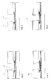
Comme illustré à la figure 2, on procède par la suite au dépôt d'une couche (10) de benzocyclobutène (BCB), ou d'un éventuel matériau équivalent, possédant une permittivité relative inférieure à 3. Ce dépôt est effectué par un procédé dit de "dépôt par rotation", également appelé "Spin on deposition". L'épaisseur déposée est voisine de 20 micromètres.As illustrated in FIG. 2, a layer is subsequently deposited (10) benzocyclobutene (BCB), or a possible equivalent material, having a relative permittivity of less than 3. This deposition is carried out by a process known as "spin deposit", also called "Spin on deposition". The thickness deposited is close to 20 micrometers.
On procède par la suite à un nettoyage de la face supérieure (11) de la couche (10) de BCB. Ce nettoyage, effectué avec un bain approprié, assure le nettoyage et la préparation de la face supérieure (11) de la couche de BCB (10).Thereafter, the upper face (11) of the layer is cleaned. (10) of BCB. This cleaning, carried out with an appropriate bath, ensures the cleaning and preparing the upper face (11) of the BCB layer (10).
Comme illustré à la figure 3, on procède par la suite au dépôt d'une couche (12) formant un masque dur au-dessus de la couche de BCB (10). Cette couche (12) présente une épaisseur de l'ordre de 200 Å. Le matériau employé est préférentiellement du carbure de silicium (SiC), mais il pourrait être également du SiOC, SiN, Si3N4, SiON, SiO4, SiO2, Cr ou de l'Y2 O3 ou tout autre matériau, dès lors que la sélectivité de gravure par rapport au matériau de la couche inférieure est au moins de 10 : 1. Cette couche (12) de masque dur peut être déposée par un procédé de dépôt chimique en phase vapeur assisté par plasma, ou PECVD pour "Plasma Enhanced Chemical Vapor Deposition".As illustrated in FIG. 3, a layer (12) forming a hard mask is then deposited on top of the BCB layer (10). This layer (12) has a thickness of the order of 200 Å. The material used is preferably silicon carbide (SiC), but it could also be SiOC, SiN, Si 3 N 4 , SiON, SiO 4 , SiO 2 , Cr or Y 2 O 3 or any other material, since the etching selectivity with respect to the material of the lower layer is at least 10: 1. This layer (12) of hard mask can be deposited by a chemical vapor deposition process assisted by plasma, or PECVD for "Plasma Enhanced Chemical Vapor Deposition".
Par la suite, on réalise une ouverture (13) dans le masque dur (12), comme illustré à la figure 4, par un procédé de lithographie et une gravure chimique appropriée utilisant un procédé par voie humide tel qu'un bain à base d'acide hypophosphorique à la température de 180°C, si le masque dur est composé de nitrure de silicium, ou une gravure sèche par plasma utilisant un gaz réactif comportant du fluorine tel que le CF4 :H2 par exemple.Thereafter, an opening (13) is made in the hard mask (12), as illustrated in FIG. 4, by a lithography process and an appropriate chemical etching using a wet process such as a bath based on hypophosphoric acid at a temperature of 180 ° C., if the hard mask is composed of silicon nitride, or a dry etching by plasma using a reactive gas comprising fluorine such as CF 4 : H 2 for example.
Par la suite, on procède comme illustré à la figure 5, à la gravure de la couche de BCB (10), à l'aplomb du plot métallique de connexion (4), de manière à former le trou d'interconnexion (14), également appelé via. La gravure de la couche de BCB peut s'effectuer notamment par l'emploi d'un mélange de gaz tel que le mélange Ar/CF4/O2 ou bien encore par un plasma radiofréquence utilisant d'autres réactants.Thereafter, one proceeds as illustrated in FIG. 5, to the etching of the BCB layer (10), directly above the metal connection pad (4), so as to form the interconnection hole (14) , also called via. The etching of the BCB layer can be carried out in particular by the use of a gas mixture such as the Ar / CF 4 / O 2 mixture or even by a radiofrequency plasma using other reactants.
Par la suite, comme illustré à la figure 6, on procède à l'élimination du masque dur qui demeurait sur les parties restantes de la couche de BCB (10). L'élimination de ce masque dur s'effectue par décapage, grâce à l'emploi d'une solution composée de Ce(SO4)2; 2(NH4)2SO4 : HClO4 : Eau désionisée si le masque dur est en chrome par exemple. Le masque dur peut également ne pas être éliminé, et donc conservé sur la couche (10) de BCB, en fonction du matériau qui le constitue, et notamment s'il s'agit de SiC, SiN ou SiON par exemple.Thereafter, as illustrated in FIG. 6, the hard mask which remains on the remaining parts of the BCB layer (10) is removed. This hard mask is removed by pickling, using a solution composed of Ce (SO4) 2 ; 2 (NH4) 2 SO 4 : HClO 4 : Deionized water if the hard mask is in chromium for example. The hard mask may also not be eliminated, and therefore stored on the layer (10) of BCB, depending on the material which constitutes it, and in particular if it is SiC, SiN or SiON for example.
On peut procéder par la suite à un nettoyage du trou d'interconnexion (14) selon différents procédés. Ainsi, il peut s'agir d'un nettoyage par voie chimique, mettant en oeuvre un mélange semi-aqueux non corrosif. On peut également assurer un nettoyage par voie sèche, en utilisant un plasma d'argon, sous une puissance de l'ordre de 300 kilowatts, en soumettant la zone (14) à des ondes radiofréquences pendant une durée voisine de la minute, et à température ambiante.You can then clean the interconnection hole (14) according to different procedures. So it can be a chemical cleaning, using a non-corrosive semi-aqueous mixture. We can also ensure dry cleaning, using an argon plasma, under a power of the order of 300 kilowatts, subjecting the zone (14) to waves radiofrequencies for a period close to one minute, and at temperature room.
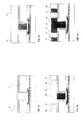
Comme illustré à la figure 7, on procède par la suite au dépôt d'une couche (15) barrière à la diffusion du cuivre. Cette couche (15) est préférentiellement en en un alliage de Titane et Tungstène, ou bien en une superposition de Titane et de Nitrure de Titane, ou bien encore de Tantale et de Nitrure de Tantale. Cette couche (15) peut également être réalisée en Nitrure de Tungstène, ou bien par une simple couche de Tungstène, de Molybdène, d'Osmium, ou de Ruthénium. Cette couche (15), d'une épaisseur comprise entre 100 et 400 Å, peut être déposée par différentes techniques, et notamment par pulvérisation, procédé également connu sous l'abréviation de PVD - IMP pour "Physical Vapor Deposition - Ionized Metal Plasma", ou par des techniques de dépôt chimique en phase vapeur connue sous le nom de CVD « Chemical Vapor Deposition» et ALD « Atomic Layer Déposition ».As illustrated in FIG. 7, a layer is subsequently deposited (15) barrier to copper diffusion. This layer (15) is preferably made of in an alloy of Titanium and Tungsten, or in a superposition of Titanium and Titanium nitride, or even tantalum and tantalum nitride. This layer (15) can also be made of Tungsten Nitride, or else by a simple layer of Tungsten, Molybdenum, Osmium, or Ruthenium. This layer (15), with a thickness between 100 and 400 Å, can be deposited by different techniques, and in particular by spraying, a process also known as the abbreviation for PVD - IMP for "Physical Vapor Deposition - Ionized Metal Plasma ", or by chemical vapor deposition techniques known as name of CVD “Chemical Vapor Deposition” and ALD “Atomic Layer Deposition ”.
Comme illustré à la figure 8, on procède par la suite au dépôt d'une couche (16) amorce de cuivre. Cette couche amorce (16) peut être déposée par différentes techniques, et notamment par pulvérisation, procédé également connu sous l'abréviation de PVD - IMP pour "Physical Vapor Deposition - Ionized Metal Plasma", ou par des techniques de dépôt chimique en phase vapeur connue sous le nom de CVD « Chemical Vapor Deposition» et ALD « Atomic Layer Deposition La couche ainsi obtenue présente une épaisseur comprise typiquement entre 500 et 2000 Å.As illustrated in FIG. 8, a layer is subsequently deposited (16) copper primer. This primer layer (16) can be deposited by different techniques, and in particular by spraying, a process also known as the abbreviation for PVD - IMP for "Physical Vapor Deposition - Ionized Metal Plasma ", or by chemical vapor deposition techniques known as name of CVD “Chemical Vapor Deposition” and ALD “Atomic Layer Deposition The layer thus obtained has a thickness typically between 500 and 2000 Å.
Par la suite, et comme illustré à la figure 9, on procède à une étape d'enrichissement de la couche amorce (16) par voie électrolytique. On peut utiliser un bain des sels de cuivre, tels que CuSO4:5H2O. On peut également procéder par apport d'un agent réducteur tel que du diméthylamineborane, en substitution du courant électrolytique.Thereafter, and as illustrated in FIG. 9, a step of enriching the primer layer (16) is carried out by electrolytic means. One can use a bath of copper salts, such as CuSO 4 : 5H 2 O. One can also proceed by adding a reducing agent such as dimethylamineborane, in substitution for the electrolytic current.
Cette étape d'enrichissement permet de combler les espaces entre les ílots de cuivre qui ont été préalablement déposés pour former la couche amorce. La surface de la couche amorce (16) est donc ainsi lissée, ce qui favorise l'étape ultérieure de dépôt électrolytique. Cette étape permet d'augmenter l'épaisseur de la couche amorce à l'intérieur de la via et plus particulièrement sur les faces intérieures et au fond du trou d'interconnexion.This enrichment step makes it possible to fill the spaces between the islands of copper which have been previously deposited to form the primer layer. The surface the primer layer (16) is thus smoothed, which favors the subsequent step of electrolytic deposition. This step increases the thickness of the layer primer inside the via and more particularly on the interior faces and bottom of the interconnecting hole.
Par la suite, comme illustré à la figure 10, on dépose sur les faces (17) de la couche amorce (16) parallèles au substrat, une couche (18) de résine photonégative. Ce dépôt (20) a également eu lieu dans le fond (19) du trou d'interconnexion, mais pas sur les parois verticales (21) de ce même trou. Cette couche (18,20) de résine photonégative présente une épaisseur de l'ordre de 5 000 Å.Thereafter, as illustrated in FIG. 10, the surfaces (17) of the primer layer (16) parallel to the substrate, a resin layer (18) photonegative. This deposit (20) also took place in the bottom (19) of the hole interconnection, but not on the vertical walls (21) of this same hole. This layer (18,20) of photonegative resin has a thickness of the order of 5,000 Å.
Par la suite, comme illustré à la figure 11, on procède à l'élimination de la couche (20) de résine photo négative située au fond (17) du trou d'interconnexion (14). Le reste (18) de la résine photo-négative n'est pas éliminée par suite du processus de photo exposition ce qui durcit la résine exposée.Thereafter, as illustrated in FIG. 11, the process of eliminating the layer (20) of photo negative resin located at the bottom (17) of the interconnection hole (14). The remainder (18) of the photo-negative resin is not removed as a result of photo exposure process which hardens the exposed resin.
Par la suite, on procède à une étape de nettoyage par application d'une solution non corrosive pour le cuivre, de manière à obtenir un état de surface optimal en ce qui concerne le fond (19) du trou d'interconnexion ainsi que ses parois latérales (21). Le bain utilisé est une solution aqueuse et peut contenir des molécules inhibitrices de corrosion telles que du benzotriazole.Thereafter, a cleaning step is carried out by applying a non-corrosive solution for copper, so as to obtain a surface finish optimal with regard to the bottom (19) of the interconnection hole as well as its side walls (21). The bath used is an aqueous solution and may contain corrosion inhibiting molecules such as benzotriazole.
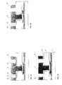
Comme illustré à la figure 12, on procède par la suite à un dépôt électrolytique de cuivre, de manière à assurer un remplissage (22) du trou d'interconnexion (14) par une technique connue sous le nom « electroplating ». Cette technique est basée sur l'utilisation d'un bain d'électrolytes dont la formulation est judicieusement définie pour obtenir une qualité de Cuivre optimale, à savoir une résistivité avant croissance des grains lors d'un recuit compris entre 1,9µΩ.cm et 2,3µΩ.cm et préférentiellement compris entre 2µΩ.cm et 2,15µΩ.cm. Par ailleurs, la définition du dépôt est directement fonction de la géométrie de la cellule électrochimique, de la distance entre la cathode et l'anode, de la forme et des caractéristiques de chaque électrode ainsi que de la zone et de la surface sur laquelle on va déposer. Les bains utilisés peuvent être par exemple ceux commercialisés sous la dénomination "Cu VIAFORM" par la société ENTHONE, ou "Cu GLEAM ELECTRODEPOSIT 6000" par la société SHIPLEY. As illustrated in figure 12, one proceeds thereafter to a deposit copper electrolytic so as to fill the hole (22) interconnection (14) by a technique known as "electroplating". This technique is based on the use of an electrolyte bath, the formulation is judiciously defined to obtain a quality of Copper optimal, i.e. resistivity before grain growth during annealing between 1.9µΩ.cm and 2.3µΩ.cm and preferably between 2µΩ.cm and 2.15µΩ.cm. Furthermore, the definition of deposit is directly dependent on the geometry of the electrochemical cell, the distance between the cathode and the anode, the shape and characteristics of each electrode as well as the area and the surface on which we are going to deposit. The baths used can be for example those marketed under the name "Cu VIAFORM" by the company ENTHONE, or "Cu GLEAM ELECTRODEPOSIT 6000" by the company SHIPLEY.
Par la suite on peut procéder à une étape de décontamination, permettant d'éliminer toute trace de cuivre qui serait susceptible de venir migrer dans le substrat ou dans tout autre partie sur laquelle les ions de cuivre ont pu se déposer. Cette étape de décontamination permet notamment de nettoyer l'arrière du substrat, ainsi que les zones périphériques du substrat. Parmi ces zones périphériques, on entend les faces latérales du substrat, perpendiculaires au plan principal du substrat ainsi que les arêtes du substrat sur lesquelles ont pu venir s'accumuler des dépôts superflus de cuivre liés au processus de dépôt du cuivre selon la technique utilisée.Then we can proceed to a decontamination step, allowing to eliminate any trace of copper which might migrate into the substrate or any other part on which the copper ions may have deposited. This decontamination step notably makes it possible to clean the back of the substrate, as well as the peripheral areas of the substrate. Among these peripheral areas, hear the lateral faces of the substrate, perpendicular to the main plane of the substrate as well as the edges of the substrate on which deposits may have accumulated copper superfluous linked to the copper deposition process according to the technique used.
Cette étape de décontamination s'effectue par voie chimique et humide au moyen d'outil permettant le traitement face par face du substrat, en utilisant un bain contenant un mélange de péroxyde d'hydrogène et d'acide sulfurique.This decontamination step is carried out by chemical and wet methods. tool means allowing the face-to-face treatment of the substrate, using a bath containing a mixture of hydrogen peroxide and sulfuric acid.
Par la suite, on procède comme illustré à la figure 13 à l'élimination par décapage du masque de résine photo négative qui protégeait la couche amorce de cuivre au-dessus des zones de BCB (10).Thereafter, we proceed as illustrated in FIG. 13 to the elimination by stripping of the negative photo resin mask which protected the primer layer from copper above the BCB zones (10).
On procède par la suite à une étape de nettoyage par application d'un bain non corrosif pour le cuivre, de manière à éliminer toute trace de résine sur la couche amorce (10), en vue de faciliter le dépôt des couches ultérieures.A cleaning step is then carried out by applying a bath. non-corrosive to copper, so as to eliminate all traces of resin on the primer layer (10), in order to facilitate the deposition of the subsequent layers.
On procède par la suite à une étape dite de "recuit", permettant de réorganiser la structure cristalline du cuivre (22) déposé dans le trou d'interconnexion (14), en faisant croítre la taille des grains élémentaires cristallins. Cette étape utilise une technique connue sous le nom de "RTP" pour "Rapid Thermal Processing" pendant laquelle le composant est soumis à une température de l'ordre de 150 à 400° C, voisine préférentiellement de 300°C, pendant une durée de 10 secondes à 30 minutes et préférentiellement pendant 5 minutes. Le composant est maintenu sous une atmosphère d'un gaz inerte ou bien sous vide évitant toute oxydation et diffusion de l'oxygène dans le milieu cristallin du cuivre. La définition des paramètres est judicieusement choisie pour obtenir une qualité de Cuivre optimale à savoir une résistivité après croissance des grains compris entre 1,7µΩ.cm et 2µΩ.cm mais préférentiellement compris entre 1,72µΩ.cm et 1,82µΩ.cm.We then proceed to a step called "annealing", allowing to reorganize the crystal structure of the copper (22) deposited in the interconnection hole (14), increasing the size of the elementary crystalline grains. This step uses a technique known as "RTP" for "Rapid Thermal Processing" during which the component is subjected to a temperature of the order of 150 to 400 ° C, preferably around 300 ° C, for a period of 10 seconds to 30 minutes and preferably for 5 minutes. The component is kept under an atmosphere of an inert gas or under vacuum avoiding any oxidation and diffusion of oxygen in the crystal medium of copper. The definition of parameters is judiciously chosen to obtain an optimal quality of Copper namely a resistivity after growth of the grains of between 1.7 μΩ.cm and 2µΩ.cm but preferably between 1.72µΩ.cm and 1.82µΩ.cm.
On procède ensuite à un étalement par effet centrifuge soit d'hexaméthyledisilazane (HMDS) soit le divinyltétramethyldisilazane (DVTMDS). Ceci permet d'optimiser l'état de surface des flancs verticaux de la résine qui sera déposée ultérieurement, et dans laquelle pourront diffuser l'HDMS ou le DVTMDS lors des étapes de recuit, car ces additifs abaissent la tension de surface de cette résine. Ce traitement favorise une meilleure adhésion du cuivre sur les flancs verticaux de la résine déposée ultérieurement, et qui forment les parois de la via (14).One then proceeds to a spreading by centrifugal effect either hexamethyledisilazane (HMDS) or divinyltetramethyldisilazane (DVTMDS). This makes it possible to optimize the surface condition of the vertical sides of the resin which will be subsequently filed, and in which the HDMS or the DVTMDS during the annealing stages, because these additives lower the surface tension of this resin. This treatment promotes better adhesion of copper to vertical sides of the subsequently deposited resin, which form the walls of the via (14).
Par la suite, on procède au dépôt d'une couche (25) de résine supérieure, comme illustrée à la figure 14. Cette résine (25) est du type photosensible positive, pour permettre les lithographies ultérieures. Cette résine (25) résiste aux chimies acides des dépôts électrolytiques.Subsequently, a layer (25) of upper resin is deposited, as illustrated in FIG. 14. This resin (25) is of the positive photosensitive type, to allow subsequent lithographies. This resin (25) resists chemistry acids from electrolytic deposits.
La couche (25) de résine supérieure ainsi déposée présente une épaisseur comprise entre 10 et 50 microns, préférentiellement comprise entre 20 et 40 microns, en fonction de la hauteur des spires du composant inductif.The upper resin layer (25) thus deposited has a thickness between 10 and 50 microns, preferably between 20 and 40 microns, depending on the height of the turns of the inductive component.
Par la suite, comme illustré à la figure 15, on procède à la gravure de cette couche de résine supérieure (25) pour définir entre les zones restantes (27) des canaux (28,29) qui recevront ultérieurement le cuivre qui formera les spires du composant inductif. Cette gravure s'effectue par un procédé de lithographie standard.Thereafter, as illustrated in FIG. 15, one proceeds to the engraving of this upper resin layer (25) to define between the remaining areas (27) channels (28,29) which will subsequently receive the copper which will form the turns of the inductive component. This engraving is carried out by a lithography process standard.
Par la suite, et comme illustré à la figure 16, on procède à un dépôt électrolytique de cuivre, au-dessus de la couche amorce (16). On notera que l'épaisseur déposée dans les canaux périphériques (28) est la même que celle dans le canal (29) situé à l'aplomb du trou d'interconnexion (4), de sorte que la croissance est sensiblement similaire. Le dépôt électrolytique du cuivre peut dans ce cas précisément se faire au moyen d'un outil de dépôt électrochimique utilisant une anode soluble de cuivre et un bain chimique choisi parmi les différents producteurs tels que le bain «Cu gleam electrodeposit 6000» commercialisé par la société Shipley. Le dépôt de cuivre remplit typiquement entre 70% et 90% des canaux (29), de manière à donner des épaisseurs de cuivre pour les spires supérieures à 10 micromètres.Thereafter, and as illustrated in FIG. 16, a deposit is made. copper electrolytic, above the primer layer (16). Note that the thickness deposited in the peripheral channels (28) is the same as that in the channel (29) located directly above the interconnection hole (4), so that the growth is substantially similar. The electrolytic deposition of copper can in this case precisely be done by means of an electrochemical deposition tool using a soluble copper anode and a chemical bath chosen from the different producers such as the “Cu gleam electrodeposit 6000” bath marketed by the Shipley company. The copper deposit typically fills between 70% and 90% of channels (29), so as to give copper thicknesses for the turns larger than 10 micrometers.
Par la suite, on procède à une étape de décontamination identique à celle
décrite à l'étape n° 16.Thereafter, a decontamination step identical to that is carried out.
described in
Par la suite, on procède à l'élimination des zones (27) de résine supérieure qui définissaient les différents canaux (28,29). L'élimination de cette résine (27) permet de libérer l'espace (32) entre spires (30-31), de manière à limiter la capacité entre spires. Cette élimination permet également de rendre accessible les couches métalliques (16,15) situées entre les spires (30-31) en vue de leur future élimination.Thereafter, the upper resin zones (27) are removed, which defined the different channels (28,29). Removal of this resin (27) frees the space (32) between turns (30-31), so as to limit the capacity between turns. This elimination also makes it possible to make the layers accessible. metal (16,15) located between the turns (30-31) for their future elimination.
Par la suite, on procède comme déjà évoqué à l'étape n° 18 à une étape de nettoyage par l'application d'un bain non corrosif pour le cuivre afin de retirer tous les résidus engendrés par l'étape de lithographie dont le procédé chimique peut utiliser un composé d'amines et de molécules anti-corrosives du cuivre choisi parmi les fabricants de tels produits comme le produit ACT-970 de la société Ashland.Thereafter, we proceed as already mentioned in step No. 18 to a step of cleaning by applying a non-corrosive copper bath to remove all the residues generated by the lithography step, the chemical process of which can use a compound of amines and anti-corrosion molecules of the chosen copper among the manufacturers of such products as the company's product ACT-970 Ashland.
Par la suite, on procède comme illustré à la figure 18, à une gravure humide anisotrope de la couche amorce de cuivre (16) , par exemple grâce à un bain d'acide sulfurique, ou un bain d'acide nitrique incluant du benzotriazole.Thereafter, as illustrated in FIG. 18, a wet etching is carried out. anisotropic of the copper primer layer (16), for example by means of a bath sulfuric acid, or a nitric acid bath including benzotriazole.
Par la suite, on procède comme illustré à la figure 19 à la gravure de la couche (15) barrière à la diffusion du cuivre qui est dépendant du choix du matériau de barrière de diffusion du cuivre. A titre d'exemple, lorsque la couche barrière de diffusion est une superposition de deux couches de Titane et de Nitrure de Titane, cette barrière de diffusion peut être gravée par une solution aqueuse composée d'éthylène diamine tétra acétique acide (EDTA) et de peroxyde d'hydrogène selon un ratio de 2 pour 1, à une température comprise entre 45°C et 90°C et préférentiellement, voisine de 65°C. Mais cet exemple n'est pas limitatif et d'autres bains chimiques peuvent être utilisés selon l'état de l'art de la technique.Thereafter, as illustrated in FIG. 19, the engraving of the layer (15) barrier to the diffusion of copper which is dependent on the choice of copper diffusion barrier material. For example, when the layer diffusion barrier is a superposition of two layers of Titanium and Nitride of Titanium, this diffusion barrier can be etched with an aqueous solution composed of ethylene diamine tetra acetic acid (EDTA) and peroxide of hydrogen in a ratio of 2 to 1, at a temperature between 45 ° C and 90 ° C and preferably around 65 ° C. But this example is not limiting and other chemical baths can be used according to the state of the art.
De la sorte, les différentes spires (30) et la partie centrale (31) du micro-composant inductif sont donc électriquement indépendantes.In this way, the different turns (30) and the central part (31) of the micro-component inductive are therefore electrically independent.
Par la suite, on procède à une étape de recuit analogue à celle décrite à l'étape n° 19.Thereafter, an annealing step similar to that described in step is carried out. n ° 19.
Par la suite, on procède à une étape de nettoyage par un bain non corrosif
pour le cuivre tel qu'analogue à celui décrit dans les étapes n° 18 et 26. Thereafter, a cleaning step is carried out using a non-corrosive bath.
for copper as analogous to that described in
Il ressort de ce qui précède que le procédé conforme à l'invention permet d'obtenir des micro-composants inductifs qui présentent un très fort facteur de qualité, du fait d'un éloignement maítrisé entre le substrat et le plan principal du micro-composant inductif. Typiquement, les facteurs de qualité obtenus sont supérieures à 40, à des fréquences de l'ordre de 2 GigaHertz.It appears from the above that the process according to the invention allows to obtain inductive micro-components which have a very high factor of quality, due to a controlled distance between the substrate and the main plane of the inductive micro-component. Typically, the quality factors obtained are greater than 40, at frequencies of the order of 2 GigaHertz.
La décomposition du dépôt électrolytique de cuivre en deux étapes distinctes permet d'assurer une optimisation de la régularité de la forme des différentes spires sans augmentation du coût de fabrication, et ainsi donc une bonne reproductibilité du procédé conduisant à la réalisation de micro-composant possédant des caractéristiques électriques très proches de celles définies lors de la conception et donc des performances électriques attendues.Decomposition of the electrolytic deposit of copper in two distinct stages allows to optimize the regularity of the shape of the different turns without increasing the manufacturing cost, and thus therefore good reproducibility of the process leading to the production of micro-component having electrical characteristics very close to those defined during design and therefore expected electrical performance.
Par ailleurs l'avantage de cette présente invention est de maítriser les interfaces entre les différentes couches de matériaux déposés et formés ce qui a pour conséquence une nette amélioration des performances du dispositif et une nette réduction des sources de défectivité.Furthermore the advantage of this present invention is to control the interfaces between the different layers of materials deposited and formed which has as a consequence a marked improvement in the performance of the device and a marked reduction in sources of defect.
Claims (27)
Applications Claiming Priority (2)
| Application Number | Priority Date | Filing Date | Title |
|---|---|---|---|
| FR0115456 | 2001-11-29 | ||
| FR0115456A FR2832852B1 (en) | 2001-11-29 | 2001-11-29 | METHOD FOR MANUFACTURING AN ELECTRONIC COMPONENT INCORPORATING AN INDUCTIVE MICRO-COMPONENT |
Publications (1)
| Publication Number | Publication Date |
|---|---|
| EP1328012A1 true EP1328012A1 (en) | 2003-07-16 |
Family
ID=8869930
Family Applications (1)
| Application Number | Title | Priority Date | Filing Date |
|---|---|---|---|
| EP02356230A Withdrawn EP1328012A1 (en) | 2001-11-29 | 2002-11-18 | Method of manufactoring an electronic device comprising an inductive mirco component |
Country Status (5)
| Country | Link |
|---|---|
| US (1) | US6727138B2 (en) |
| EP (1) | EP1328012A1 (en) |
| JP (1) | JP2003234412A (en) |
| CA (1) | CA2409237A1 (en) |
| FR (1) | FR2832852B1 (en) |
Families Citing this family (11)
| Publication number | Priority date | Publication date | Assignee | Title |
|---|---|---|---|---|
| US8041719B2 (en) * | 2003-05-06 | 2011-10-18 | Symantec Corporation | Personal computing device-based mechanism to detect preselected data |
| US20050110142A1 (en) * | 2003-11-26 | 2005-05-26 | Lane Michael W. | Diffusion barriers formed by low temperature deposition |
| US7074719B2 (en) * | 2003-11-28 | 2006-07-11 | International Business Machines Corporation | ALD deposition of ruthenium |
| KR100577528B1 (en) * | 2003-12-30 | 2006-05-10 | 매그나칩 반도체 유한회사 | Method of manufacturing a inductor in a semiconductor device |
| US20060197183A1 (en) * | 2005-03-01 | 2006-09-07 | International Business Machines Corporation | Improved mim capacitor structure and process |
| US7367113B2 (en) * | 2006-04-06 | 2008-05-06 | United Microelectronics Corp. | Method for fabricating a transformer integrated with a semiconductor structure |
| CN100454516C (en) * | 2006-04-17 | 2009-01-21 | 联华电子股份有限公司 | A method for manufacturing of transformer integrated in the semiconductor integral circuit structure |
| US20100015329A1 (en) * | 2008-07-16 | 2010-01-21 | National Semiconductor Corporation | Methods and systems for packaging integrated circuits with thin metal contacts |
| JP5498808B2 (en) * | 2010-01-28 | 2014-05-21 | ルネサスエレクトロニクス株式会社 | Manufacturing method of semiconductor device |
| CN102496616B (en) * | 2011-11-28 | 2016-04-27 | 日月光半导体制造股份有限公司 | There is semiconductor element and the manufacture method thereof of integrated passive element |
| US9330989B2 (en) * | 2012-09-28 | 2016-05-03 | Taiwan Semiconductor Manufacturing Company, Ltd. | System and method for chemical-mechanical planarization of a metal layer |
Citations (3)
| Publication number | Priority date | Publication date | Assignee | Title |
|---|---|---|---|---|
| US5874883A (en) * | 1995-07-18 | 1999-02-23 | Nec Corporation | Planar-type inductor and fabrication method thereof |
| US6030877A (en) * | 1997-10-06 | 2000-02-29 | Industrial Technology Research Institute | Electroless gold plating method for forming inductor structures |
| EP1039544A1 (en) * | 1999-03-23 | 2000-09-27 | Memscap | Monolithic integrated circuit comprising an inductor and a method of fabricating the same |
Family Cites Families (3)
| Publication number | Priority date | Publication date | Assignee | Title |
|---|---|---|---|---|
| US6326301B1 (en) * | 1999-07-13 | 2001-12-04 | Motorola, Inc. | Method for forming a dual inlaid copper interconnect structure |
| US6573822B2 (en) * | 2001-06-18 | 2003-06-03 | Intel Corporation | Tunable inductor using microelectromechanical switches |
| US6586322B1 (en) * | 2001-12-21 | 2003-07-01 | Taiwan Semiconductor Manufacturing Co., Ltd. | Method of making a bump on a substrate using multiple photoresist layers |
-
2001
- 2001-11-29 FR FR0115456A patent/FR2832852B1/en not_active Expired - Fee Related
-
2002
- 2002-10-21 CA CA002409237A patent/CA2409237A1/en not_active Abandoned
- 2002-11-18 EP EP02356230A patent/EP1328012A1/en not_active Withdrawn
- 2002-11-25 US US10/303,401 patent/US6727138B2/en not_active Expired - Lifetime
- 2002-11-28 JP JP2002346551A patent/JP2003234412A/en not_active Withdrawn
Patent Citations (3)
| Publication number | Priority date | Publication date | Assignee | Title |
|---|---|---|---|---|
| US5874883A (en) * | 1995-07-18 | 1999-02-23 | Nec Corporation | Planar-type inductor and fabrication method thereof |
| US6030877A (en) * | 1997-10-06 | 2000-02-29 | Industrial Technology Research Institute | Electroless gold plating method for forming inductor structures |
| EP1039544A1 (en) * | 1999-03-23 | 2000-09-27 | Memscap | Monolithic integrated circuit comprising an inductor and a method of fabricating the same |
Also Published As
| Publication number | Publication date |
|---|---|
| JP2003234412A (en) | 2003-08-22 |
| US20030098766A1 (en) | 2003-05-29 |
| CA2409237A1 (en) | 2003-05-29 |
| US6727138B2 (en) | 2004-04-27 |
| FR2832852A1 (en) | 2003-05-30 |
| FR2832852B1 (en) | 2004-02-27 |
Similar Documents
| Publication | Publication Date | Title |
|---|---|---|
| EP1927129B1 (en) | Electroplating method for coating a substrate surface with a metal | |
| EP0351001A1 (en) | Method for making a semi-conductor device with at least one level of interconnection with small dimensioned via holes | |
| EP2279290B1 (en) | Electroplating composition and process for coating a semiconductor substrate using said composition | |
| KR20110051251A (en) | Barrier layer removal method and apparatus | |
| JP2012064945A (en) | Semiconductor device and method for manufacturing the same | |
| FR2929449A1 (en) | METHOD OF FORMING A STARTING LAYER OF DEPOSITION OF A METAL ON A SUBSTRATE | |
| US11043379B2 (en) | Conformal carbon film deposition | |
| EP1328012A1 (en) | Method of manufactoring an electronic device comprising an inductive mirco component | |
| EP1320123A1 (en) | Manufacturing process of an electronic device comprising an inductive micro component | |
| EP1030353A1 (en) | Anisotropic plasma etching of a dielectric, organic polymer material | |
| EP1316974A1 (en) | Fabrication process for electronic component with incorporated microinductance | |
| FR2785721A1 (en) | Semiconductor structure, with a metal via and a metal wiring, is produced by partial via hole etching and then simultaneously etching a wiring trench and the via hole remainder | |
| FR2763424A1 (en) | Dual damascene process for integrated circuits | |
| FR2855324A1 (en) | Fabrication of a semiconductor device incorporating a copper interconnection by means of a masking technique using an insulating film of a low constant dielectric material | |
| EP0435717A1 (en) | Process for interconnecting of metallic layers in multilayer circuits of an electronic board and the board produced by the process | |
| WO2021009459A1 (en) | Process for hydrophilically bonding substrates | |
| JP2937998B1 (en) | Wiring manufacturing method | |
| EP2843693A1 (en) | Method for producing a conductive pad on a conductive member | |
| FR2620860A1 (en) | METHOD AND STRUCTURE FOR OBTAINING LOW RESISTANCE OF CONTACT WITH ALUMINUM AND ITS ALLOYS WITH SELECTIVE TUNGSTEN DEPOSITION | |
| KR100434700B1 (en) | Method for forming copper of semiconductor device | |
| FR2961220A1 (en) | Composition, useful for filling semiconductor substrate cavity, comprises copper ions, copper complexing agent containing compound comprising aliphatic polyamine, preferably ethylenediamine, thiodiglycolic acid and optionally buffer system | |
| TW457683B (en) | Cu damascene processes preventing hillock on the surface | |
| JPS6113375B2 (en) | ||
| TW477050B (en) | Method to avoid generating aluminum whisker defect in the manufacturing process of W-plug structure | |
| EP0994506A1 (en) | Method of making memory cell capacitor |
Legal Events
| Date | Code | Title | Description |
|---|---|---|---|
| PUAI | Public reference made under article 153(3) epc to a published international application that has entered the european phase |
Free format text: ORIGINAL CODE: 0009012 |
|
| AK | Designated contracting states |
Designated state(s): AT BE BG CH CY CZ DE DK EE ES FI FR GB GR IE IT LI LU MC NL PT SE SK TR |
|
| AX | Request for extension of the european patent |
Extension state: AL LT LV MK RO SI |
|
| 17P | Request for examination filed |
Effective date: 20040108 |
|
| AKX | Designation fees paid |
Designated state(s): AT BE BG CH CY CZ DE DK EE ES FI FR GB GR IE IT LI LU MC NL PT SE SK TR |
|
| STAA | Information on the status of an ep patent application or granted ep patent |
Free format text: STATUS: THE APPLICATION IS DEEMED TO BE WITHDRAWN |
|
| 18D | Application deemed to be withdrawn |
Effective date: 20050601 |