EP1327897A2 - Optical power splitter having a stabilizing waveguide - Google Patents
Optical power splitter having a stabilizing waveguide Download PDFInfo
- Publication number
- EP1327897A2 EP1327897A2 EP02027669A EP02027669A EP1327897A2 EP 1327897 A2 EP1327897 A2 EP 1327897A2 EP 02027669 A EP02027669 A EP 02027669A EP 02027669 A EP02027669 A EP 02027669A EP 1327897 A2 EP1327897 A2 EP 1327897A2
- Authority
- EP
- European Patent Office
- Prior art keywords
- waveguide
- optical
- section
- input
- stabilizing
- Prior art date
- Legal status (The legal status is an assumption and is not a legal conclusion. Google has not performed a legal analysis and makes no representation as to the accuracy of the status listed.)
- Withdrawn
Links
Images




Classifications
-
- G—PHYSICS
- G02—OPTICS
- G02B—OPTICAL ELEMENTS, SYSTEMS OR APPARATUS
- G02B6/00—Light guides; Structural details of arrangements comprising light guides and other optical elements, e.g. couplings
- G02B6/10—Light guides; Structural details of arrangements comprising light guides and other optical elements, e.g. couplings of the optical waveguide type
- G02B6/12—Light guides; Structural details of arrangements comprising light guides and other optical elements, e.g. couplings of the optical waveguide type of the integrated circuit kind
- G02B6/122—Basic optical elements, e.g. light-guiding paths
- G02B6/125—Bends, branchings or intersections
-
- G—PHYSICS
- G02—OPTICS
- G02B—OPTICAL ELEMENTS, SYSTEMS OR APPARATUS
- G02B6/00—Light guides; Structural details of arrangements comprising light guides and other optical elements, e.g. couplings
- G02B6/10—Light guides; Structural details of arrangements comprising light guides and other optical elements, e.g. couplings of the optical waveguide type
- G02B6/12—Light guides; Structural details of arrangements comprising light guides and other optical elements, e.g. couplings of the optical waveguide type of the integrated circuit kind
- G02B2006/12133—Functions
- G02B2006/1215—Splitter
-
- G—PHYSICS
- G02—OPTICS
- G02B—OPTICAL ELEMENTS, SYSTEMS OR APPARATUS
- G02B6/00—Light guides; Structural details of arrangements comprising light guides and other optical elements, e.g. couplings
- G02B6/10—Light guides; Structural details of arrangements comprising light guides and other optical elements, e.g. couplings of the optical waveguide type
- G02B6/12—Light guides; Structural details of arrangements comprising light guides and other optical elements, e.g. couplings of the optical waveguide type of the integrated circuit kind
- G02B2006/12166—Manufacturing methods
- G02B2006/12195—Tapering
Definitions
- the present invention relates to a planar waveguide device, and more particularly to an optical power splitter utilizing a Y-branch optical waveguide.
- An optical waveguide device includes an optical waveguide core through which an optical signal is transmitted by experiencing total internal reflection in the optical waveguide core, and a clad surrounding the optical waveguide core.
- Representative examples of optical waveguide devices include a planar waveguide device fabricated in a semiconductor manufacturing process and an optical fiber manufactured by melting an optical fiber preform.
- Planar waveguide devices include optical power splitter/couplers that divide or couple the power of the optical signal and wavelength division multiplexer/demultiplexers that multiplex or demultiplex channels constituting the optical signal according to wavelengths of the optical signal.
- the optical power splitter may include a tapered waveguide, that enlarges field distribution of an input optical signal, and a Y-branch optical waveguide having a pair of output waveguide branches, that splits the enlarged optical signal and outputs it through ends of the output waveguide branches.
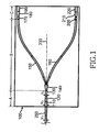
- FIG. 1 is a schematic plan view of a conventional optical power splitter utilizing a Y-branch optical waveguide.
- the conventional optical power splitter 100 generally includes an input section 101, a branching section 102, and an output section 103. Further, the optical power splitter 100 is constructed so that both sides are symmetric with reference to an axis 230 of the optical power splitter 100.
- the input section 101 includes an input waveguide section 110.
- the input waveguide section 110 receives an optical signal through its input end connected with an outer waveguide 250 and controls the device length of the optical power splitter 100.
- the input waveguide section 110 has a width 104 that can optimize the mode field diameter (MFD) of the outer waveguide 250 and the mode field diameter of the input waveguide section 110 and that enables single-mode propagation and low-loss insertion of the optical signal. That is, in order to minimize the coupling loss of the optical signal, the input waveguide section 110 enlarges the field distribution of the optical signal and functions as a coupling section that enables single-mode propagation and low-loss insertion of the optical signal.
- the outer waveguide 250 is a waveguide that constitutes an optical fiber or a planar waveguide device.
- the branching section 102 includes a first tapered waveguide section 140, and first and second waveguide branches 150 and 160.
- the first tapered waveguide section 140 receives the optical signal through its input end connected with the input waveguide section 110, and the width of the first tapered waveguide section 140 gradually increases in the direction toward which the optical signal propagates.
- the first and second waveguide branches 150 and 160 extend from the output end of the first tapered waveguide section 140 symmetrically with reference to the axis 230.
- the output section 103 includes second and third auxiliary waveguide sections 170 and 200, second and third tapered waveguide sections 180 and 210, and first and second output waveguide sections 190 and 220.
- the second auxiliary waveguide section 170 controls the device length of the optical power splitter 100 and connects the first waveguide branch 150 and the second tapered waveguide section 180 with each other.
- the second tapered waveguide section 180 receives a first branched optical signal through its input end connected with the second auxiliary waveguide section 170, and the width of the second tapered waveguide section 180 gradually increases in the direction toward which the first branched optical signal propagates.
- the first output waveguide section 190 receives the first branched optical signal through its input end and outputs the first branched optical signal through its output end.
- the third auxiliary waveguide section 200 controls the device length of the optical power splitter 100 and connects the second waveguide branch 160 to the third tapered waveguide section 210.
- the third tapered waveguide section 210 receives a second branched optical signal through its input end connected with the third auxiliary waveguide section 200, and the width of the third tapered waveguide section 210 gradually increases in the direction toward which the second branched optical signal propagates.
- the second output waveguide section 220 receives the second branched optical signal through its input end and outputs the second branched optical signal through its output end.
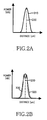
- FIGs. 2A and 2B are graphs describing the mode matching in the case where an optical signal is input in alignment with the axis of the optical power splitter 100, that is, the case where the optical signal is input into the optical power splitter 100 in such a manner that the field distribution of the optical signal has a shape both sides of which are symmetric with reference to the axis 230.
- the graph shown in FIG. 2A shows a first field distribution 310 in the input waveguide section 110 at the input end of the input waveguide section 110, which means a field distribution of the optical signal propagating through the input waveguide section 110 directly after passing the input end of the input waveguide section 110.
- the first field distribution 310 is arranged symmetrically with reference to the axis 230. This mode matching maximizes the coupling efficiency between the input waveguide section 110 and the optical signal.
- the graph shown in FIG. 2B shows a third field distribution 320 in the first tapered waveguide section 140 and a fourth field distribution 330 in the first and second waveguide branches 150 and 160, at the output end of the first tapered waveguide section 140.
- the first field distribution 310 and the fourth field distribution 330 are arranged symmetrically with reference to the axis 230. These mode matches maximize the coupling efficiency of the optical signal between the first tapered waveguide section 140 and the first and second waveguide branches 150 and 160.
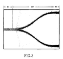
- FIG. 3 is a view showing an intensity distribution of the optical signal propagating through the optical power splitter 100 in the mode match state.
- sections 301, 302, and 303 represent the intensity distributions of the input section 101, branching section 102, and output section 103, respectively.
- FIGs. 4A and 4B are graphs illustrating mode mismatch in the case where an optical signal is input in misalignment with the axis 230 of the optical power splitter 100. That is, these figures illustrate the case where the optical signal is input into the optical power splitter 100 in such a manner that the field distribution of the optical signal has a shape in which the sides are nonsymmetrical with reference to the axis 230.
- the graph illustrated in FIG. 4A shows a fifth field distribution 340 in the input waveguide section 110 at the input end of the input waveguide section 110. As shown, a center line of the fifth field distribution 340 is not aligned with the axis 230. This mode mismatch degrades the coupling efficiency between the input waveguide section 110 and the optical signal.
- the graph illustrated in FIG. 4B shows a sixth field distribution 350 in the first tapered waveguide section 140 and a seventh field distribution 360 in the first and second waveguide branches 150 and 160, at the input end of the first tapered waveguide section 140.
- the center lines of the sixth field distribution 350 and the seventh field distribution 360 are not aligned with each other. This mode mismatch degrades the coupling efficiency between the first tapered waveguide section 140 and the first and second waveguide branches 150 and 160.
- FIG. 5 illustrates an intensity distribution of an optical signal propagating through the optical power splitter 100 in the mode mismatch state.
- sections 304, 305, and 306 represent the intensity distributions of the input section 101, branching section 102, and output section 103, respectively.
- the optical signal shakes while passing through the input section 101, thereby having an effect on the branching section B, which consequently causes the mode mismatch as shown in FIG. 4B.
- FIG. 6 is a graph illustrating loss corresponding to the mode mismatch of the optical signal input to the optical power splitter 100
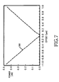
- FIG. 7 is a graph illustrating uniformity according to the mode mismatch of the optical signal input to the optical power splitter 100.
- FIG. 6 illustrates a first output curve 370 representing the output of the first output waveguide section 190 according to the mode mismatch of the optical signal and a second output curve 380 representing the output of the second output waveguide section 220 according to the mode mismatch of the optical signal.
- the difference of the outputs between the first output curve 370 and the second output curve 380 becomes significantly larger.
- FIG. 7 illustrates a uniformity curve 390 representing the difference between the outputs of the first and second output waveguide sections 190 and 220 according to the mode mismatch of the optical signal. As shown, the difference between the outputs of the first and second output waveguide sections 190 and 220 abruptly increases as the mode mismatch increases.
- the conventional optical power splitter utilizing a Y-branch optical waveguide is problematic in that, the larger the mode mismatch, the larger the difference between the outputs of the first and second output waveguide sections 190 and 220. Moreover, the difference between the outputs of the first and second output waveguide sections 190 and 220 according to the mode mismatch of the optical signal further increases when the optical signal is a multi-channel signal.
- the present invention provides an optical power splitter 400 that can operate stably even when there is a mode mismatch between an input optical signal and the optical power splitter.
- the present invention is an optical power splitter 400 comprising a semiconductor substrate, an optical waveguide stacked on the semiconductor substrate, and a clad surrounding the optical waveguide.
- the optical waveguide functions as a medium through which an optical signal transmits, the signal having a plurality of channels according to wavelengths.
- the optical waveguide comprises several components. At the input is an input waveguide section 410 through which the optical signal is input from an outer waveguide 550. Connected to the input waveguide section 410 is a tapered waveguide section 440 that gradually increases in width. First 450 and second 460 waveguide branches in a branching section 403 extend from an output end of the tapered waveguide section 440 and output first and second branched optical signals.
- a stabilizing waveguide section 430 is disposed between the input waveguide section 410 and the tapered waveguide section 440, the stabilizing waveguide section having a length 407 and a width 406 capable of being preset to values which enable stabilizing of a shaking of the optical signal that is generated by a mode mismatch between the optical signal and the input waveguide section 410.
- FIG. 8 illustrates an optical power splitter utilizing a Y-branch optical waveguide according to a preferred embodiment of the present invention.
- the optical power splitter 400 generally includes an input section 401, a stabilizing section 402, a branching section 403, and an output section 404. Further, the optical power splitter 400 has a construction both sides of which are symmetric with respect to axis 530 of the optical power splitter 400.
- the input section 401 includes an input waveguide section 410 having width 405 and a first tapered waveguide section 420.
- the input waveguide section 410 receives an optical signal through its input end that is connected with an outer waveguide 550.
- the input waveguide section 410 has characteristics of a single-mode propagation and low-loss insertion.
- the first tapered waveguide section 420 receives the optical signal through its input end connected with the input waveguide section 410, and the width of the first tapered waveguide section 420 gradually decreases in the direction toward which the optical signal propagates.
- the input waveguide section 410 has a width 405 that optimizes mode field diameters of the outer waveguide 550 and the input waveguide section 410.
- the outer waveguide 550 is a waveguide that constitutes an optical fiber or a planar waveguide device.
- the stabilizing section 402 comprises stabilizing waveguide section 430 having a predetermined width 406 and length 407.
- the first tapered waveguide section 420 is disposed between the input waveguide section 410 and the stabilizing waveguide section 430.
- the coupling efficiency is highly dependent on alignment and the tapering of the first tapered waveguide section 420 gradually decreases its width thus allowing gradual confinement of the propagating light which relieves alignment concerns.
- the stabilizing waveguide section 430 is disposed between the first tapered waveguide section 420 that tapers increasingly and a second tapered waveguide section 440 that tapers decreasingly and has a width 406 and length 407 which in combination stabilize the shaking of the optical signal, which shaking may be generated due to mode mismatch between the optical signal and the input waveguide section 410.
- the width 406 of the stabilizing waveguide section 430 is smaller than the width 105 of 130, since the smaller the width 406 of the stabilizing waveguide section 430, within a predetermined limit, the greater the stabilization of the optical signal.
- the branching section 403 includes the second tapered waveguide section 440, and a first and a second waveguide branche 450 and 460.
- the second tapered waveguide section 440 receives the optical signal through its input end connected with the stabilizing waveguide section 430, and the width of the second tapered waveguide section 440 gradually increases in the direction toward which the optical signal propagates.
- the first and second waveguide branches 450 and 460 extend from the output end of the second tapered waveguide section 440 symmetrically with reference to the axis 530.
- the output section 404 includes a first and a second auxiliary waveguide section 470 and 500, a third and a fourth tapered waveguide section 480 and 510, and a first and a second output waveguide section 490 and 520.
- the first auxiliary waveguide section 470 controls the device length of the optical power splitter 400 and links the first waveguide branch 450 and the third tapered waveguide section 480 with each other.
- the third tapered waveguide section 480 receives a first branched optical signal through its input end connected with the first auxiliary waveguide section 470, and the width of the third tapered waveguide section 480 gradually increases in the direction toward which the first branched optical signal propagates.
- the first output waveguide section 490 receives the first branched optical signal through its input end and outputs the first branched optical signal through its output end.
- the second auxiliary waveguide section 500 controls the device length of the optical power splitter 400 and links the second waveguide branch 460 and the fourth tapered waveguide section 510 with each other.
- the fourth tapered waveguide section 510 receives a second branched optical signal through its input end connected with the second auxiliary waveguide section 500, and the width of the fourth tapered waveguide section 510 gradually increases in the direction toward which the second branched optical signal propagates.
- the second output waveguide section 520 receives the second branched optical signal through its input end and outputs the second branched optical signal through its output end.
- FIGs. 9A and 9B are graphs illustrating a process of stabilizing the field distribution of an optical signal in the case where the optical signal is input in misalignment with the axis 530 of the optical power splitter 400, that is, the case where the optical signal is input into the optical power splitter 400 in such a manner that the field distribution of the optical signal has a shape both sides of which are nonsymmetrical with reference to the axis 530.
- the graph illustrated in FIG. 9A shows a first field distribution 610 in the input waveguide section 410 at the input end of the input waveguide section 410, which is a field distribution of the optical signal propagating through the input waveguide section 410 directly after passing through the input end of the input waveguide section 410.
- a center line of the first field distribution 610 is not aligned with the axis 530. This mode mismatch degrades the coupling efficiency between the input waveguide section 410 and the optical signal.
- the graph illustrated in FIG. 9B shows a second field distribution 620 in the second tapered waveguide section 440 and a third field distribution 630 in the first and second waveguide branches 450 and 460, at the output end of the second tapered waveguide section 440.
- the second field distribution 620 and the third field distribution 630 are arranged symmetrically with reference to the axis 530. These mode matches maximize the coupling efficiency of the optical signal between the second tapered waveguide section 440 and the first and second waveguide branches 450 and 460.
- FIG. 10 illustrates an intensity distribution of the optical signal propagating through the optical power splitter 400.
- sections 1001, 1002, 1003, and 1004 represent the intensity distributions of the input section 401, stabilizing section 402, branching section 403, and output section 404, respectively.
- FIG. 10 illustrates the optical signal shaking while passing through the input section 401 but stably propagating through the stabilizing section 402. That is, the optical signal initially propagating while shaking is gradually stabilized while passing through the stabilizing section 402. This stabilization of the optical signal results in the mode match illustrated in FIG. 9B.
- FIG. 11 is a graph illustrating the change of outputs according to the mode mismatch of the optical signal input to the optical power splitter 400
- FIG. 12 is a graph illustrating the change of uniformity according to the mode mismatch of the optical signal input to the optical power splitter 400.
- the stabilizing waveguide section 430 of the present invention has a width 406 of 3 ⁇ m and a length 407 of 2000 ⁇ m.
- FIG. 11 shows a first output curve 640 representing the output of the first output waveguide section 490 according to the mode mismatch of the optical signal and a second output curve 650 representing the output of the second output waveguide section 520 according to the mode mismatch of the optical signal.
- the difference of the outputs shown by the first output curve 640 and the second output curve 650 becomes only slightly larger for an optical power splitter having a stabilizing waveguide according to the present invention.
- FIG. 12 is a graph illustrating a first uniformity curve 660 representing the difference between the outputs of the first and second output waveguide sections 490 and 520 according to the mode mismatch of the optical signal. As shown in FIG. 12, the difference between the outputs of the first and second output waveguide sections 490 and 520 slightly increases as the mode mismatch increases for an optical power splitter having a stabilizing waveguide according to the present invention.
- FIG. 13 is a graph illustrating the change of uniformity according to the mode mismatch of the optical signal input to the optical power splitter 400 and the width 406 of the stabilizing waveguide section 430.
- FIG. 13 shows first to sixth uniformity curves 660, 670, 680, 690, 700, and 710 representing the difference between the outputs of the first and second output waveguide sections 490 and 520 according to the mode mismatch of the optical signal, respectively.
- FIG. 13 shows first to sixth uniformity curves 660, 670, 680, 690, 700, and 710 representing the difference between the outputs of the first and second output waveguide sections 490 and 520 according to the mode mismatch of the optical signal, respectively.
- the first to sixth uniformity curves 660, 670, 680, 690, 700, and 710 represent the difference between the outputs of the first and second output waveguide sections 490 and 520 in the case where the width 406 of the stabilizing waveguide section 430 is 3 ⁇ m, 4 ⁇ m, 5 ⁇ m, 6 ⁇ m, 7 ⁇ m, and 8 ⁇ m, respectively.
- the length 407 of the stabilizing waveguide section 430 is 2000 ⁇ m.
- FIG. 13 shows that the smaller the width 406 of the stabilizing waveguide section 430 according to the present invention, the smoother the corresponding uniformity curve.
- FIGs. 14 and 15 are graphs illustrating the change of uniformity according to the width 406 and length 407 of the stabilizing waveguide section 430 according to the present invention.
- FIG. 14 shows seventh to twelfth uniformity curves 720, 730, 740, 750, 760, and 770 representing the difference between the outputs of the first and second output waveguide sections 490 and 520 according to the width 406 of the stabilizing waveguide section 430.
- the seventh to twelfth uniformity curves 720, 730, 740, 750, 760, and 770 represent the difference between the outputs of the first and second output waveguide sections 490 and 520 in the case where the length 407 of the stabilizing waveguide section 430 is 0 ⁇ m, 1000 ⁇ m, 2000 ⁇ m, 3000 ⁇ m, 4000 ⁇ m, and 5000 ⁇ m, respectively.
- the error in the mode matching of the optical signal is 0.3 ⁇ m.
- the width 406 of the stabilizing waveguide section 430 according to the present invention the substantially smaller the difference between the outputs of the first and second output waveguide sections 490 and 520.
- FIG. 15 illustrates thirteenth to seventeenth uniformity curves 780, 790, 800, 810, and 820 representing the difference between the outputs of the first and second output waveguide sections 490 and 520 according to the length 407 of the stabilizing waveguide section 430.
- the thirteenth to seventeenth uniformity curves 780, 790, 800, 810, and 820 represent the difference between the outputs of the first and second output waveguide sections 490 and 520 in the case where the width 406 of the stabilizing waveguide section 430 is 3 ⁇ m, 4 ⁇ m, 5 ⁇ m, 6 ⁇ m, and 7 ⁇ m, respectively.
- the error in the mode matching of the optical signal is 0.3 ⁇ m.
- FIG. 15 illustrates that the larger the length 407 of the stabilizing waveguide section 430 according to the present invention, the substantially smaller the difference between the outputs of the first and second output waveguide sections 490 and 520.
- the width and length of the stabilizing wave guide can be adjusted, thereby enabling the optical power splitter to stably operate even when there is a mode mismatch between an input optical signal and the optical power splitter.
Landscapes
- Physics & Mathematics (AREA)
- Engineering & Computer Science (AREA)
- Microelectronics & Electronic Packaging (AREA)
- General Physics & Mathematics (AREA)
- Optics & Photonics (AREA)
- Optical Integrated Circuits (AREA)
Abstract
Description
Claims (12)
- An optical power splitter comprising a semiconductor substrate, an optical waveguide stacked on the semiconductor substrate, and a clad surrounding the optical waveguide, the optical waveguide functioning as a medium through transmits which an optical signal having a plurality of channels according to wavelengths, the optical waveguide comprising:an input waveguide section having a width through which the optical signal is inputted from an outer waveguide;a tapered waveguide section having a gradually increasing width;a first and second waveguide branch extending from an output end of the tapered waveguide section and outputting a first and second branched optical signal, respectively; anda stabilizing waveguide section disposed between the input waveguide section and the tapered waveguide section, the stabilizing waveguide section having a length and a width capable of stabilizing a shaking of the optical signal that is generated by a mode mismatch between the optical signal and the input waveguide section.
- An optical power splitter as claimed in claim 1, wherein the width of the stabilizing waveguide section is smaller than the width of the input waveguide section, the input waveguide section having characteristics of a single-mode propagation and low-loss insertion.
- An optical power splitter as claimed in claim 1, wherein the width of the stabilizing waveguide section is a value between 3 and 8 µm.
- An optical power splitter as claimed in claim 3, wherein the length of the stabilizing waveguide section is a value between 0 and 2000 µm.
- An optical power splitter as claimed in claim 1, wherein the width of the input waveguide section optimizes a mode field diameter of the outer waveguide and the input waveguide section.
- An optical power splitter as claimed in claim 5, wherein the outer waveguide is one of an optical fiber and a planar waveguide device.
- An optical waveguide for stabilizing an optical power splitter, the optical waveguide functioning as a medium through which transmits an optical signal having a plurality of channels according to wavelengths, the optical waveguide comprising:wherein said stabilizing section is capable of stabilizing a shaking of the optical signal input to the input waveguide from the outer waveguide, said shaking being generated by a mode mismatch between the optical signal and the input waveguide.an input section comprising an input waveguide having a predetermined width and a mode field, said mode field having a diameter, said input waveguide connected to an outer waveguide having a mode field;a branching section comprising a Y-branch optical waveguide having a first and second branch, said first and second branch being symmetric with respect to an axis of the optical splitter; anda stabilizing section comprising a stabilizing waveguide having a predetermined width and length and being disposed between the input section and the branching section,
- An optical waveguide as claimed in claim 7, wherein the width of the stabilizing waveguide is a value between 3 and 8µm.
- An optical waveguide as claimed in claim 7, wherein the length of the stabilizing waveguide is a value between 0 and 2000 µm.
- An optical waveguide as claimed in claim 7, wherein:said stabilizing waveguide has characteristics of a single-mode propagation and low-loss insertion; andsaid width of the stabilizing waveguide section is smaller than the width of the input waveguide.
- An optical waveguide as claimed in claim 7, wherein the width of the input waveguide optimizes the mode field diameter of the outer waveguide and of the input waveguide.
- An optical waveguide as claimed in claim 11, wherein the outer waveguide is one of an optical fiber and a planar waveguide device.
Applications Claiming Priority (2)
| Application Number | Priority Date | Filing Date | Title |
|---|---|---|---|
| KR10-2002-0002147A KR100417002B1 (en) | 2002-01-14 | 2002-01-14 | Optical power splitter with stabilizing waveguide |
| KR2002002147 | 2002-01-14 |
Publications (2)
| Publication Number | Publication Date |
|---|---|
| EP1327897A2 true EP1327897A2 (en) | 2003-07-16 |
| EP1327897A3 EP1327897A3 (en) | 2004-07-14 |
Family
ID=19718461
Family Applications (1)
| Application Number | Title | Priority Date | Filing Date |
|---|---|---|---|
| EP02027669A Withdrawn EP1327897A3 (en) | 2002-01-14 | 2002-12-12 | Optical power splitter having a stabilizing waveguide |
Country Status (4)
| Country | Link |
|---|---|
| US (1) | US6961497B2 (en) |
| EP (1) | EP1327897A3 (en) |
| JP (1) | JP2003207663A (en) |
| KR (1) | KR100417002B1 (en) |
Cited By (1)
| Publication number | Priority date | Publication date | Assignee | Title |
|---|---|---|---|---|
| WO2005111681A1 (en) * | 2004-05-14 | 2005-11-24 | Omron Corporation | Optical branching device |
Families Citing this family (12)
| Publication number | Priority date | Publication date | Assignee | Title |
|---|---|---|---|---|
| JP3543137B2 (en) * | 2002-04-01 | 2004-07-14 | Tdk株式会社 | Optical branch circuit |
| CN100406936C (en) * | 2003-05-16 | 2008-07-30 | 日立化成工业株式会社 | Optical waveguide structure |
| US7532792B2 (en) * | 2006-08-28 | 2009-05-12 | Crystal Fibre A/S | Optical coupler, a method of its fabrication and use |
| EP2131220A4 (en) * | 2007-03-27 | 2013-04-03 | Sumitomo Osaka Cement Co Ltd | Method of adjusting optical axis of optical waveguide element, and optical waveguide element |
| KR101008271B1 (en) * | 2008-05-31 | 2011-01-14 | 오종찬 | Pole mosquito net with backrest and shade |
| CN103837930A (en) * | 2012-11-26 | 2014-06-04 | 宜兴新崛起光集成芯片科技有限公司 | Low-loss waveguide type optical divider |
| CN103424805A (en) * | 2012-12-20 | 2013-12-04 | 上海信电通通信建设服务有限公司 | Y-bifurcation-structured 1 * 2 optical power splitter |
| CN105116491B (en) * | 2015-09-22 | 2018-04-24 | 东南大学 | A kind of silicon substrate groove waveguides integrated-type optical power distributor |
| US10033148B2 (en) * | 2016-02-04 | 2018-07-24 | Lawrence Livermore National Security, Llc | Waveguide design for line selection in fiber lasers and amplifiers |
| US10348050B2 (en) | 2016-02-04 | 2019-07-09 | Lawrence Livermore National Security, Llc | Nd3+fiber laser and amplifier |
| CN106054339B (en) * | 2016-08-16 | 2018-10-23 | 河南仕佳光子科技股份有限公司 | A kind of design method of the insensitive optical branching device of ultra-wide spectrum wavelength |
| CN116724258A (en) * | 2021-01-18 | 2023-09-08 | 艾尤纳公司 | Double-layer optical coupling configuration between photonic integrated circuit and external single-mode fiber |
Family Cites Families (25)
| Publication number | Priority date | Publication date | Assignee | Title |
|---|---|---|---|---|
| JPS55147604A (en) * | 1979-05-08 | 1980-11-17 | Toshiba Corp | Production of photo distributor |
| JP3066866B2 (en) * | 1989-10-25 | 2000-07-17 | 三菱瓦斯化学株式会社 | Optical splitter |
| US5048909A (en) * | 1990-07-27 | 1991-09-17 | At&T Bell Laboratories | Adiabatic reflection apparatus |
| JP3102874B2 (en) * | 1990-11-05 | 2000-10-23 | 日本板硝子株式会社 | Y-branch optical circuit |
| JP2809517B2 (en) * | 1990-12-10 | 1998-10-08 | 日本電信電話株式会社 | Branch and multiplex optical waveguide circuit |
| CA2120792C (en) * | 1993-07-16 | 2006-05-09 | Eisuke Sasaoka | Optical waveguide device |
| DE69417986T2 (en) * | 1993-11-01 | 1999-09-30 | Sumitomo Electric Industries, Ltd. | Optical branch element |
| US5408556A (en) * | 1993-12-06 | 1995-04-18 | Kaptron, Inc. | 1 X N splitter for single-mode fibers and method of construction |
| DE19514042A1 (en) * | 1995-04-13 | 1996-10-17 | Sel Alcatel Ag | Optical splitter |
| JPH095549A (en) * | 1995-06-19 | 1997-01-10 | Sumitomo Electric Ind Ltd | Optical circuit and method for manufacturing the same |
| US6236782B1 (en) * | 1995-08-29 | 2001-05-22 | Arroyo Optics, Inc. | Grating assisted coupler devices |
| JPH09189817A (en) * | 1996-01-09 | 1997-07-22 | Mitsubishi Gas Chem Co Inc | Optical waveguide for optical splitter |
| US5745619A (en) * | 1996-06-07 | 1998-04-28 | Lucent Technologies Inc. | Low-loss optical power splitter for high-definition waveguides |
| US5799119A (en) * | 1996-07-03 | 1998-08-25 | Northern Telecom Limited | Coupling of strongly and weakly guiding waveguides for compact integrated mach zehnder modulators |
| JP2993433B2 (en) * | 1996-08-02 | 1999-12-20 | 日本電気株式会社 | Optical coupler |
| US5864644A (en) * | 1997-07-21 | 1999-01-26 | Lucent Technologies Inc. | Tapered fiber bundles for coupling light into and out of cladding-pumped fiber devices |
| JPH11133253A (en) * | 1997-11-04 | 1999-05-21 | Nippon Telegr & Teleph Corp <Ntt> | Array waveguide type wavelength multiplexer / demultiplexer |
| US6434302B1 (en) * | 1998-03-04 | 2002-08-13 | Jds Uniphase Corporation | Optical couplers for multimode fibers |
| JP2000137128A (en) * | 1998-11-04 | 2000-05-16 | Nok Corp | Optical branch waveguide and optical modulator |
| JP3448518B2 (en) | 1999-07-30 | 2003-09-22 | 古河電気工業株式会社 | Array waveguide diffraction grating |
| JP2001091774A (en) * | 1999-09-24 | 2001-04-06 | Oki Electric Ind Co Ltd | Optically integrated circuit device |
| JP2001235645A (en) * | 2000-02-25 | 2001-08-31 | Furukawa Electric Co Ltd:The | Optical waveguide circuit |
| JP2001305357A (en) * | 2000-04-19 | 2001-10-31 | Oki Electric Ind Co Ltd | Wavelength demultiplexer |
| KR100416997B1 (en) * | 2001-07-23 | 2004-02-05 | 삼성전자주식회사 | Y-branch optical waveguide and multi-stage optical power splitter using that |
| US20030133663A1 (en) * | 2002-01-16 | 2003-07-17 | Jds Uniphase Corporation | Integrated optical splitter |
-
2002
- 2002-01-14 KR KR10-2002-0002147A patent/KR100417002B1/en not_active Expired - Fee Related
- 2002-11-25 US US10/303,228 patent/US6961497B2/en not_active Expired - Fee Related
- 2002-12-12 EP EP02027669A patent/EP1327897A3/en not_active Withdrawn
-
2003
- 2003-01-08 JP JP2003002000A patent/JP2003207663A/en active Pending
Cited By (2)
| Publication number | Priority date | Publication date | Assignee | Title |
|---|---|---|---|---|
| WO2005111681A1 (en) * | 2004-05-14 | 2005-11-24 | Omron Corporation | Optical branching device |
| US7362933B2 (en) | 2004-05-14 | 2008-04-22 | Omron Corporation | Optical branching unit |
Also Published As
| Publication number | Publication date |
|---|---|
| US6961497B2 (en) | 2005-11-01 |
| JP2003207663A (en) | 2003-07-25 |
| EP1327897A3 (en) | 2004-07-14 |
| US20030133662A1 (en) | 2003-07-17 |
| KR100417002B1 (en) | 2004-02-05 |
| KR20030061982A (en) | 2003-07-23 |
Similar Documents
| Publication | Publication Date | Title |
|---|---|---|
| CA2734614C (en) | Optical mode transformer, in particular for coupling an optical fiber and a high-index contrast waveguide | |
| CN102159975B (en) | Method and apparatus for efficient coupling between silicon photonic chip and optical fiber | |
| US6961497B2 (en) | Optical power splitter having a stabilizing waveguide | |
| US20040105677A1 (en) | Optical demultiplexer, optical multi-/demultiplexer, and optical device | |
| US20060115215A1 (en) | Dual "cheese wedge" silicon taper waveguide | |
| US20160116680A1 (en) | Light coupling structure and optical device including a grating coupler | |
| US20240393532A1 (en) | Relaxed tolerance adiabatic coupler for optical interconnects | |
| JP2003057464A (en) | Y-branch optical waveguide and multi-stage optical power splitter using the same | |
| US12422622B2 (en) | Photonic systems comprising an asymmetric coupler and methods of fabrication | |
| US6934427B2 (en) | High density integrated optical chip with low index difference waveguide functions | |
| CN104122621B (en) | Compound Optical Combiner | |
| CN114616500B (en) | Multicore fiber and fan-out assembly | |
| US6801692B2 (en) | Optical coupling structure | |
| KR100417001B1 (en) | Optical power splitter with assistant waveguide | |
| JP7501651B2 (en) | Optical lateral input/output circuit and optical connector | |
| US6731841B1 (en) | Folded waveguide optical devices | |
| US6453094B1 (en) | All fiber DWDM multiplexer and demultiplexer | |
| US7706644B2 (en) | Offset launch mode from nanotaper waveguide into multimode fiber | |
| JP2007148290A (en) | Directional optical coupler | |
| CN100394230C (en) | Multi-channel arrayed waveguide diffraction grating multiplexer/demultiplexer and method for connecting arrayed waveguide and output waveguide | |
| EP4394465A2 (en) | Methods and apparatus for optical coupler | |
| JP2005301301A (en) | Optical coupler | |
| WO2025115180A1 (en) | Lateral light input/output circuit | |
| JP2004252142A (en) | Optical device | |
| CN119439372A (en) | A four-port beam splitter, optical module and output light splitting ratio adjustment method |
Legal Events
| Date | Code | Title | Description |
|---|---|---|---|
| PUAI | Public reference made under article 153(3) epc to a published international application that has entered the european phase |
Free format text: ORIGINAL CODE: 0009012 |
|
| AK | Designated contracting states |
Designated state(s): AT BE BG CH CY CZ DE DK EE ES FI FR GB GR IE IT LI LU MC NL PT SE SI SK TR |
|
| AX | Request for extension of the european patent |
Extension state: AL LT LV MK RO |
|
| PUAL | Search report despatched |
Free format text: ORIGINAL CODE: 0009013 |
|
| AK | Designated contracting states |
Kind code of ref document: A3 Designated state(s): AT BE BG CH CY CZ DE DK EE ES FI FR GB GR IE IT LI LU MC NL PT SE SI SK TR |
|
| AX | Request for extension of the european patent |
Extension state: AL LT LV MK RO |
|
| 17P | Request for examination filed |
Effective date: 20041222 |
|
| 17Q | First examination report despatched |
Effective date: 20050203 |
|
| AKX | Designation fees paid |
Designated state(s): DE FR GB |
|
| STAA | Information on the status of an ep patent application or granted ep patent |
Free format text: STATUS: THE APPLICATION IS DEEMED TO BE WITHDRAWN |
|
| 18D | Application deemed to be withdrawn |
Effective date: 20070703 |