EP1326323A2 - Switched power supply with voltage regulator having pwm with hysteretic loop controller and method for operating and using same - Google Patents
Switched power supply with voltage regulator having pwm with hysteretic loop controller and method for operating and using same Download PDFInfo
- Publication number
- EP1326323A2 EP1326323A2 EP02102334A EP02102334A EP1326323A2 EP 1326323 A2 EP1326323 A2 EP 1326323A2 EP 02102334 A EP02102334 A EP 02102334A EP 02102334 A EP02102334 A EP 02102334A EP 1326323 A2 EP1326323 A2 EP 1326323A2
- Authority
- EP
- European Patent Office
- Prior art keywords
- output
- power supply
- output voltage
- comparator
- voltage
- Prior art date
- Legal status (The legal status is an assumption and is not a legal conclusion. Google has not performed a legal analysis and makes no representation as to the accuracy of the status listed.)
- Granted
Links
- 238000000034 method Methods 0.000 title claims description 16
- 230000004044 response Effects 0.000 claims abstract description 11
- 239000003990 capacitor Substances 0.000 description 17
- 238000013500 data storage Methods 0.000 description 9
- 230000001105 regulatory effect Effects 0.000 description 5
- 230000007246 mechanism Effects 0.000 description 4
- 230000008901 benefit Effects 0.000 description 3
- 238000010586 diagram Methods 0.000 description 3
- 230000009467 reduction Effects 0.000 description 3
- 230000008859 change Effects 0.000 description 2
- 230000002159 abnormal effect Effects 0.000 description 1
- 230000009471 action Effects 0.000 description 1
- 230000000295 complement effect Effects 0.000 description 1
- 230000001276 controlling effect Effects 0.000 description 1
- 230000007547 defect Effects 0.000 description 1
- 238000001514 detection method Methods 0.000 description 1
- 238000012358 sourcing Methods 0.000 description 1
- 238000009987 spinning Methods 0.000 description 1
Images


Classifications
-
- H—ELECTRICITY
- H02—GENERATION; CONVERSION OR DISTRIBUTION OF ELECTRIC POWER
- H02M—APPARATUS FOR CONVERSION BETWEEN AC AND AC, BETWEEN AC AND DC, OR BETWEEN DC AND DC, AND FOR USE WITH MAINS OR SIMILAR POWER SUPPLY SYSTEMS; CONVERSION OF DC OR AC INPUT POWER INTO SURGE OUTPUT POWER; CONTROL OR REGULATION THEREOF
- H02M3/00—Conversion of DC power input into DC power output
- H02M3/02—Conversion of DC power input into DC power output without intermediate conversion into AC
- H02M3/04—Conversion of DC power input into DC power output without intermediate conversion into AC by static converters
- H02M3/10—Conversion of DC power input into DC power output without intermediate conversion into AC by static converters using discharge tubes with control electrode or semiconductor devices with control electrode
- H02M3/145—Conversion of DC power input into DC power output without intermediate conversion into AC by static converters using discharge tubes with control electrode or semiconductor devices with control electrode using devices of a triode or transistor type requiring continuous application of a control signal
- H02M3/155—Conversion of DC power input into DC power output without intermediate conversion into AC by static converters using discharge tubes with control electrode or semiconductor devices with control electrode using devices of a triode or transistor type requiring continuous application of a control signal using semiconductor devices only
- H02M3/156—Conversion of DC power input into DC power output without intermediate conversion into AC by static converters using discharge tubes with control electrode or semiconductor devices with control electrode using devices of a triode or transistor type requiring continuous application of a control signal using semiconductor devices only with automatic control of output voltage or current, e.g. switching regulators
Definitions
- This invention relates, in one aspect, to improvements in voltage regulator circuits and methods for operating same, and, in another aspect, to improvements in mass data storage devices, circuits, and methods, and more particularly to improvements in mass data storage devices, or the like, which include voltage regulator circuits, and methods for using and operating same.
- Switched power supplies operate by alternately switching a current onto and away from a path that includes an inductor and a capacitor.
- the capacitor is connected to one end of the inductor, and sinks and sources the current therein so that as the current is switched, the capacitor maintains the voltage on the node to which it is connected.
- the voltage can be regulated to maintain a desired value within a quiescent operating range.
- a magneto-resistive (MR) data transducer or head may be used.
- the head may be biased by a biasing circuit that maintains a normal or quiescent current in the head (or a normal or quiescent voltage across the head).
- MR heads change resistance when they are moved through changing magnetic fields.
- data which is magnetically recorded on a magnetic media such as a spinning disk or the like, passes the MR head, the changes in resistance in the head can be detected and decoded to retrieve the data.
- the MR head may actually undesirably contact a defect in the magnetic media, which may rapidly heat the MR head, and drastically change its resistance. This results in a rapid demand for current from the power supply to the head biasing circuit.
- the flight height of the head is significantly increased, such as if a dip were to occur in the magnetic disk above which the head flies. In this case, the head is unexpectedly cooled. This abnormally increases the resistance of the head, and reduces the demands on the power supply to the biasing circuit.
- the circuit when the circuit performs a read or write operation, the current demands of the DSP of the circuit are changed.
- the read operation in particular causes the DSP to perform a large amount of data processing. This large increase in processing requires that a large amount of current be supplied.
- circuit and method provide for duty cycle boost or reduction while a feedback loop is still in control of the output, and that this is performed while still keeping the fundamental switching frequency.
- a switched power supply has a switched circuit for producing an output voltage, and a circuit for generating pulse width modulated control pulses to control on and off times of the switched circuit to control a magnitude of the output voltage.
- a switched power supply has a circuit for generating pulse width modulated control pulses to control its output voltage.
- a first comparator is connected to receive the output voltage on one input and a first reference voltage on another input. When the output voltage exceeds the first reference voltage, the output of the first comparator changes state.
- a second comparator is connected to receive the output voltage on one input and a second reference voltage on another input. When the second reference voltage exceeds the output voltage, the output of the second comparator changes state.
- a circuit is then provided changing the pulse width modulated pulses to first or second width limits in response to respective changes of the output states of the first and second comparators.
- the circuit for generating pulse width modulated control pulses may include a comparator connected to receive a signal indicating an output voltage of the supply on one input, and a ramp wave signal from a ramp wave generator on another input.
- An output of the comparator is a signal containing a time width proportional to the output voltage of the supply.
- a method for operating a switched power supply.
- the method includes generating pulse width modulated control pulses to control on and off times of current switches in the supply, and modifying a width of the pulse width modulated control pulses to control a magnitude of the output voltage of the supply.
- the method also includes, in another aspect, changing a width of the pulse width modulated pulses to a first or a second width limit in response to respective changes of the output voltage beyond first and second predetermined values.
- a mass data storage device includes a switched power supply that provides power to at least one element of the device.
- the supply includes a switched circuit for producing an output voltage, and a circuit for generating pulse width modulated control pulses to control on and off times of the switching elements to control a magnitude of the output voltage.
- the device may also include a circuit for changing a width of the pulse width modulated pulses to first or second width limits in response to respective changes of the output voltage beyond first and second predetermined values.
- Figures 3A-D are a series of waveforms developed at various points in the circuit of Figure 2, for various circuit conditions, according to a preferred embodiment of the invention.
- like reference numerals are used to denote like or similar parts. Also, like reference numerals are used to denote signal waveforms and the circuit lines or locations from which they are derived.
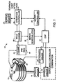
- FIG. 1 is a block diagram of a generic disk drive system 10, which represents a general environment in which the invention may be practiced.
- the system includes a magnetic media disk 12 that is rotated by a spindle motor 14 and spindle driver circuit 16.
- a data transducer or head 18 is locatable along selectable radial tracks (not shown) of the disk 12 by a voice coil motor 22.
- the head 18 may be a magneto-resistive (MR) head, but the environment is not limited thereto.
- the radial tracks may contain magnetic states that contain information about the tracks, such as track identification data, location information, synchronization data, as well as user data, and so forth.
- the head 18 is used both to record user data to and read user data back from the disk, as well as to detect signals that identify the tracks and sectors at which data is written, and to detect servo bursts that enable the head to be properly laterally aligned with the tracks of the disk.
- Analog electrical signals that are generated by the head 18 in response to the magnetic signals recorded on the disk are preamplified by a preamplifier 24 for delivery to read channel circuitry 26.
- Servo signals are detected and demodulated by one or more servo demodulator circuits 28 and processed by a digital signal processor (DSP) 30 to control the position of the head 18 via the positioning driver circuit 32.
- DSP digital signal processor
- the servo data that is read and processed may be analog data that is interpreted by the DSP 30 for positioning the head 18.
- a microcontroller 34 is typically provided to control the DSP 30, as well as an interface controller 36 to enable data to be passed to and from a host interface (not shown) in known manner.
- a data memory 38 may be provided, if desired, to buffer data being written to and read from the disk 12.
- a power supply and regulator 40 in accordance with a preferred embodiment of the invention, may be used to provide power at least to the preamplifier 24 of the mass data storage device 10 of Figure 1. It should be noted that although the power supply 40 is described and illustrated in conjunction with a mass data storage device environment, it can be equally advantageously employed in other environments, as well, as will be apparent to those skilled in the art.
- the circuit 40 is a switched power supply that provides a regulated output voltage on output line 42 with respect to a supply voltage line 44.
- the output voltage is maintained on an output capacitor 46 by sourcing a current by a PWM switching operation of FET 50 through an inductor 48 to raise the voltage, or by sinking a current by a complementary PWM switching operation of FET 52 from the inductor 48 to ground to lower the voltage.
- the FETs 50 is controlled by an anti-shoot-through circuit 58 via amplifier 56, and the FET 52 is controlled by the anti-shoot-through circuit 58 via inverter 60.
- the anti-shoot-through circuit 58 is controlled by the output of a NOR gate 62 on line 63.
- the NOR gate 62 produces a stream of pulses of pulse modulated width controlled by the output of a set-reset (SR) flip-flop (FF) 64 that is connected to a first input of the NOR gate 62.
- SR set-reset
- FF flip-flop
- the set input of the SRFF 64 is controlled by a comparator 66, which has a reference voltage applied on line 104 to its inverting input and a ramp voltage applied to its non-inverting input.
- the reference voltage as below described in detail, is derived either from the fed back output voltage on line 42 or from a switching circuit 73 for changing the pulse width modulated pulses to first or second width limits in response to respective changes in the output voltage on line 42 beyond predefined limits.
- the ramp voltage is generated by a ramp generator 68, which has a pulse stream applied on its input line 70 and is delivered on output line 69.
- the ramp waveform is illustrated by waveforms 69, the pulse stream is illustrated by waveforms 70, and the reference voltage is illustrated by waveforms 104 in Figures 3A-D. (It is noted that like reference numerals are used to denote signal waveforms and the circuit lines or locations from which they are derived.)
- the pulses on line 70 are also applied to the reset input of the SRFF 64 and to a second input of the NOR gate 62.
- the comparator 66 and the SRFF 64 serve to shape the input signal to the NOR gate 62 to provide pulses of duration on line 63 that are width controlled by the difference between the reference voltage 104 on the inverting input of the comparator 66 and the instantaneous amplitude of the ramp signal 69 generated by the ramp generator 68 with respect to the period of the pulse stream 70 on line 70.
- the longer that the instantaneous ramp voltage generated by the ramp generator 68 exceeds the reference voltage the less time the output Q of the SRFF stays high, and the less time the capacitor 46 is charged.
- the pulses on line 63 are shown by waveforms 63 in Figures 3A-D.
- the reference voltage 104 is lower than the reference voltage 104 in Figure 3B, resulting in shorter pulses 63 at the output of the NOR gate 62.
- the inverting input to the comparator 66 is generated by the output from a comparator 67.
- the comparator 67 receives the output voltage, which is fed back from the output line 42, on its inverting input through a control circuit 72.
- the output of the comparator 67 is connected through a current limiting resistor 71 to the inverting input of the comparator 66 via line 104.
- normal variations in the output voltage on line 42 can be easily compensated for by pulse width modulating the pulses applied to the inductance 48 and capacitor 46 in the output circuit.
- control circuit 72 receives the fed back output voltage on a resistor 76, which is in series with a resistor 78 that is in parallel with a capacitor 80.
- the output from the control circuit 72 is connected by a resistor 82 in series with a capacitor 84 to the inverting input of a comparator 67, which is a part of the hysteretic loop controller 65.
- the output of a soft start voltage controller 86 is applied to the non-inverting input of the comparator 67 to control the voltage applied to the comparator 66 during start-up of the circuit.
- the output voltage on line 42 is also applied to two comparators 92 and 94 in the hysteretic loop controller 65. More particularly, the fed back voltage on line 42 is applied to the inverting input of a comparator 88 and to the non-inverting input of a comparator 90.
- the non-inverting input of the comparator 88 is connected to a negative reference voltage on line 92
- the inverting input of the comparator 90 is connected to a positive reference voltage on line 94.
- the reference voltages may be of a desired value to define the control range of the hysteretic loop.
- the output of the comparator 88 controls a switch 96 and the output of the comparator 90 controls a switch 98, each connected to switch the inverting input of comparator 66, respectively to a positive voltage and to ground through resistors 100 and 102.
- the output of comparator 90 changes state to close switch 98. This pulls down line 104 to ground at the inverting input to comparator 66 through the pull-down resistor 102, as shown in Figure 3C.
- a ramp wave of maximum duty cycle is passed through the comparator, resulting in pulses of minimum duty cycle being delivered by the NOR gate 62 to lower the voltage of the output on line 42.
- the output of comparator 88 changes state to close switch 96.
- a ramp wave of minimum duty cycle is passed through the comparator, resulting in pulses of maximum duty cycle being delivered by the NOR gate 62 to raise the voltage of the output on line 42.
- the output from the comparator 90 is connected to control the voltage in the inverter 60. This raises the voltage on the gate of PMOS device 52 to turn it on, which rapidly discharges the capacitor 46 to ground until its voltage level is within the desired operating range.
- the output voltage on line 42 is maintained at its desired value by two mechanisms.
- the first mechanism is by the ordinary pulse width modulation action of the pulses at the output of the NOR gate 62.
- the second mechanism occurs if any changes in the output voltage, for example, caused by changes in the load to which the circuit is connected, cause the output voltage to exceed either limit defined by the hysteretic control loop 65. In this event, the duty cycle of the PWM control pulses is rapidly changed to an upper or lower PWM limit, to rapidly bring the output back to the desired level.
- the voltage values applied on lines 92 and 94 to the comparators 90 and 88 may be, respectively +25mV and -25mV, which is about plus and minus 1.7% of the 1.5V quiescent voltage value. If the output voltage, for instance, exceeds 1.525 volts in the positive direction, or 1.475 volts in the negative direction, the limit detection mechanisms of the hysteretic control loop 65 force the output voltage back to the quiescent value as rapidly as possible.
- the circuit and method of the invention provide for duty cycle boost or reduction while a feedback loop is still in control of the output.
- the fundamental switching frequency is continuously maintained.
Landscapes
- Engineering & Computer Science (AREA)
- Power Engineering (AREA)
- Dc-Dc Converters (AREA)
Abstract
Description
Claims (9)
- A switched power supply, comprising:a circuit for generating pulse width modulated control pulses to control a output voltage of said switched power supply;a first comparator connected to receive said output voltage on one input and a first reference voltage on another input, wherein when said output voltage exceeds said first reference voltage, an output of said first comparator changes output state;a second comparator connected to receive said output voltage on one input and a second reference voltage on another input, wherein when said second reference voltage exceeds said output voltage, an output of said second comparator changes output state;and a circuit for changing said pulse width modulated pulses to first or second width limits in response to respective changes of output states of said first and second comparators.
- The switched power supply of claim 1 wherein said circuit for generating pulse width modulated control pulses to control a magnitude of an output of said switched power supply comprises:wherein an output of said comparator is a signal containing a time width proportional to said output of said switched power supply.a comparator connected to receive on one input a signal indicating a value of an output of said switched power supply;a ramp wave generator for producing a ramp wave output connected to another input of said comparator;
- The switched power supply of claim 1 or claim 2 further comprising a power supply for said switched power supply of about 5 volts, and wherein said first and second reference voltages are respectively +25mV and -25mV.
- A method for operating a switched power supply, comprising:generating pulse width modulated control pulses to control on and off times of said switched power supply circuit;and modifying a width of said pulse width modulated control pulses to control a magnitude of said an output voltage of said switched power supply.
- The method of claim 4 further comprising changing a width of said pulse width modulated pulses to first or second width limits in response to respective changes of said output voltage beyond first and second predetermined values.
- The method of claim 5 wherein said changing a width of said pulse width modulated pulses comprises:comparing said output voltage with a first reference voltage and generating a first control output when said output voltage exceeds said first reference voltage;comparing said output voltage with a second reference voltage and generating a second control output when said second reference voltage exceeds said output voltage;and changing said pulse width modulated pulses to said first or second width limits in response to respective changes of said first and second control outputs.
- A switched power supply, comprising:a switched circuit for producing an output voltage;a circuit for generating pulse width modulated control pulses to control on and off times of said switched circuit to control a magnitude of said output voltage.
- The switched power supply of claim 7 further comprising a circuit for changing a width of said pulse width modulated pulses to first or second width limits in response to respective changes of the output voltage of said switched power supply beyond first and second predetermined values.
- The switched power supply of claim 8 wherein said circuit for changing a width of said pulse width modulated pulses comprises:a first comparator connected to receive an output voltage of said switched power supply on one input and a first reference voltage on another input, wherein when said output voltage exceeds said first reference voltage, an output of said first comparator changes output state;a second comparator connected to receive said output voltage on one input and a second reference voltage on another input, wherein when said second reference voltage exceeds said output voltage, an output of said second comparator changes output state;and a circuit for changing said pulse width modulated pulses to said first or second width limits in response to respective changes of output states of said first and second comparators.
Applications Claiming Priority (2)
| Application Number | Priority Date | Filing Date | Title |
|---|---|---|---|
| US953535 | 2001-09-11 | ||
| US09/953,535 US6617834B2 (en) | 2001-09-11 | 2001-09-11 | Switched power supply with voltage regulator having PWM with hysteretic loop controller and method for operating and using same |
Publications (3)
| Publication Number | Publication Date |
|---|---|
| EP1326323A2 true EP1326323A2 (en) | 2003-07-09 |
| EP1326323A3 EP1326323A3 (en) | 2004-10-06 |
| EP1326323B1 EP1326323B1 (en) | 2010-08-18 |
Family
ID=25494149
Family Applications (1)
| Application Number | Title | Priority Date | Filing Date |
|---|---|---|---|
| EP02102334A Expired - Lifetime EP1326323B1 (en) | 2001-09-11 | 2002-09-09 | Switched power supply with voltage regulator having pwm with hysteretic loop controller and method for operating and using same |
Country Status (4)
| Country | Link |
|---|---|
| US (1) | US6617834B2 (en) |
| EP (1) | EP1326323B1 (en) |
| JP (1) | JP2003111395A (en) |
| DE (1) | DE60237344D1 (en) |
Families Citing this family (14)
| Publication number | Priority date | Publication date | Assignee | Title |
|---|---|---|---|---|
| TWI225330B (en) * | 2003-10-31 | 2004-12-11 | Winbond Electronics Corp | Pulse width modulation power regulator and power supply system thereof |
| TWI312223B (en) * | 2003-11-14 | 2009-07-11 | Beyond Innovation Tech Co Ltd | A pulse width modulation control circuit and the loading system of its application |
| US6965223B1 (en) * | 2004-07-06 | 2005-11-15 | National Semiconductor Corporation | Method and apparatus to allow rapid adjustment of the reference voltage in a switching regulator |
| US7568117B1 (en) * | 2005-10-03 | 2009-07-28 | Zilker Labs, Inc. | Adaptive thresholding technique for power supplies during margining events |
| US7656600B2 (en) * | 2006-08-25 | 2010-02-02 | Seagate Technology Llc | Monitoring transducer potential to detect an operating condition |
| US7971076B2 (en) * | 2007-09-28 | 2011-06-28 | Infineon Technologies Ag | Circuitry and method for monitoring a supply voltage |
| US8305064B2 (en) * | 2008-12-24 | 2012-11-06 | Dora S.P.A. | Control device for a switching converter |
| US8358114B1 (en) | 2009-04-28 | 2013-01-22 | Western Digital Technologies, Inc. | Output capacitor current as feedback to control a hysteretic voltage regulator |
| US8159202B2 (en) | 2009-06-22 | 2012-04-17 | Seagate Technology Llc | Quasi-continuous voltage regulator with dual polarity outputs |
| US8232788B2 (en) * | 2009-06-22 | 2012-07-31 | Seagate Technology Llc | Quasi-continuous voltage regulator and controller |
| KR101728185B1 (en) * | 2009-10-28 | 2017-04-18 | 가부시키가이샤 한도오따이 에네루기 켄큐쇼 | Pwm limiter circuit |
| TWM412423U (en) * | 2010-08-13 | 2011-09-21 | Micro Star Int Co Ltd | Computer motherboard for reducing power consumption during sleep mode |
| US9459636B2 (en) | 2013-02-22 | 2016-10-04 | Freescale Semiconductor, Inc. | Transition control for a hybrid switched-mode power supply (SMPS) |
| US9191013B1 (en) | 2013-10-24 | 2015-11-17 | Seagate Technology Llc | Voltage compensation |
Family Cites Families (11)
| Publication number | Priority date | Publication date | Assignee | Title |
|---|---|---|---|---|
| US4477867A (en) * | 1981-08-28 | 1984-10-16 | Data General Corporation | Core saturation control circuit |
| GB8817684D0 (en) * | 1988-07-25 | 1988-09-01 | Astec Int Ltd | Power factor improvement |
| US4941076A (en) * | 1988-10-12 | 1990-07-10 | Zenith Electronics Corporation | Start-up circuit for a high voltage DC to AC converter |
| US4940929A (en) * | 1989-06-23 | 1990-07-10 | Apollo Computer, Inc. | AC to DC converter with unity power factor |
| US5166871A (en) * | 1990-08-31 | 1992-11-24 | International Business Machines Corporation | Buck switching regulator with tow control loops |
| US5406468A (en) * | 1993-09-02 | 1995-04-11 | Motorola, Inc. | Method for minimizing output transient responses in a power supply |
| US5491445A (en) * | 1994-07-05 | 1996-02-13 | Delco Electronics Corporation | Booster power converter having accelerated transient boost response |
| US5801518A (en) * | 1995-02-28 | 1998-09-01 | Seiko Instruments Inc. | Pulse frequency modulated DC-DC converter |
| US5625279A (en) * | 1996-03-28 | 1997-04-29 | Hewlett-Packard Company | DC-DC converter with dynamically adjustable characteristics |
| US5894243A (en) * | 1996-12-11 | 1999-04-13 | Micro Linear Corporation | Three-pin buck and four-pin boost converter having open loop output voltage control |
| US6104172A (en) * | 1997-07-01 | 2000-08-15 | Power-One | Power factor corrector |
-
2001
- 2001-09-11 US US09/953,535 patent/US6617834B2/en not_active Expired - Lifetime
-
2002
- 2002-09-09 DE DE60237344T patent/DE60237344D1/en not_active Expired - Lifetime
- 2002-09-09 EP EP02102334A patent/EP1326323B1/en not_active Expired - Lifetime
- 2002-09-11 JP JP2002265472A patent/JP2003111395A/en active Pending
Also Published As
| Publication number | Publication date |
|---|---|
| US20030048098A1 (en) | 2003-03-13 |
| EP1326323A3 (en) | 2004-10-06 |
| DE60237344D1 (en) | 2010-09-30 |
| US6617834B2 (en) | 2003-09-09 |
| JP2003111395A (en) | 2003-04-11 |
| EP1326323B1 (en) | 2010-08-18 |
Similar Documents
| Publication | Publication Date | Title |
|---|---|---|
| US6617834B2 (en) | Switched power supply with voltage regulator having PWM with hysteretic loop controller and method for operating and using same | |
| US6804131B2 (en) | PWM/linear driver for an electromagnetic load | |
| US6753667B2 (en) | Method and apparatus for controlling spindle motor to match plural modes of operation in a disk drive | |
| US7312944B2 (en) | Heater control method and storage apparatus | |
| US6831800B2 (en) | Boost system and method to facilitate driving a load | |
| US5706222A (en) | Multiple mode peak detector | |
| US6617817B2 (en) | Electrical time constant compensation method for switched, voltage-mode driver circuit | |
| US10410656B1 (en) | Data storage device pre-biasing a spin torque oscillator prior to a write operation | |
| US6392375B1 (en) | Method of driving with high precision a voice coil motor and related architecture | |
| US6259305B1 (en) | Method and apparatus to drive the coil of a magnetic write head | |
| US6608728B1 (en) | Magnetic disk unit | |
| US6735038B2 (en) | Supply variance compensation method for switched voltage mode voice coil motor driver circuit | |
| US12148446B1 (en) | Power improvement for minimum switching frequency operation | |
| US7839103B1 (en) | Adjustable frequency PWM driver | |
| JP2011248996A (en) | Detection device | |
| US20130120877A1 (en) | Head ic and magnetic disk apparatus having microwave assistance function | |
| JP2002245603A (en) | Magnetic recording device | |
| US7038870B2 (en) | Data storage device, data write method, and program | |
| US6975473B2 (en) | Power efficient overshoot protection during an operating mode transition | |
| US5831783A (en) | Power source control circuit for controlling an electric potential of a magnetic head and memory apparatus using such a power source control circuit | |
| US5844396A (en) | Voice coil motor drive unit for magnetic disk drive having a wave shaping unit including zener diodes with zener voltage set higher than a voltage applied to the coil in positioning the magnetic head, and lower than the voltage applied to the coil in movi | |
| JP4171158B2 (en) | Supply method of write current | |
| US6724162B2 (en) | Motor-control device enabling the rotational speed of the motor's rotor to be measured | |
| JP2565018B2 (en) | Inrush current prevention circuit | |
| US6754022B1 (en) | High-speed current driver |
Legal Events
| Date | Code | Title | Description |
|---|---|---|---|
| PUAI | Public reference made under article 153(3) epc to a published international application that has entered the european phase |
Free format text: ORIGINAL CODE: 0009012 |
|
| AK | Designated contracting states |
Designated state(s): AT BE BG CH CY CZ DE DK EE ES FI FR GB GR IE IT LI LU MC NL PT SE SK TR |
|
| AX | Request for extension of the european patent |
Extension state: AL LT LV MK RO SI |
|
| PUAL | Search report despatched |
Free format text: ORIGINAL CODE: 0009013 |
|
| AK | Designated contracting states |
Kind code of ref document: A3 Designated state(s): AT BE BG CH CY CZ DE DK EE ES FI FR GB GR IE IT LI LU MC NL PT SE SK TR |
|
| AX | Request for extension of the european patent |
Extension state: AL LT LV MK RO SI |
|
| 17P | Request for examination filed |
Effective date: 20050406 |
|
| AKX | Designation fees paid |
Designated state(s): DE FR GB |
|
| GRAP | Despatch of communication of intention to grant a patent |
Free format text: ORIGINAL CODE: EPIDOSNIGR1 |
|
| GRAC | Information related to communication of intention to grant a patent modified |
Free format text: ORIGINAL CODE: EPIDOSCIGR1 |
|
| GRAC | Information related to communication of intention to grant a patent modified |
Free format text: ORIGINAL CODE: EPIDOSCIGR1 |
|
| GRAC | Information related to communication of intention to grant a patent modified |
Free format text: ORIGINAL CODE: EPIDOSCIGR1 |
|
| GRAS | Grant fee paid |
Free format text: ORIGINAL CODE: EPIDOSNIGR3 |
|
| GRAA | (expected) grant |
Free format text: ORIGINAL CODE: 0009210 |
|
| AK | Designated contracting states |
Kind code of ref document: B1 Designated state(s): DE FR GB |
|
| REG | Reference to a national code |
Ref country code: GB Ref legal event code: FG4D |
|
| REF | Corresponds to: |
Ref document number: 60237344 Country of ref document: DE Date of ref document: 20100930 Kind code of ref document: P |
|
| PLBE | No opposition filed within time limit |
Free format text: ORIGINAL CODE: 0009261 |
|
| STAA | Information on the status of an ep patent application or granted ep patent |
Free format text: STATUS: NO OPPOSITION FILED WITHIN TIME LIMIT |
|
| 26N | No opposition filed |
Effective date: 20110519 |
|
| REG | Reference to a national code |
Ref country code: DE Ref legal event code: R097 Ref document number: 60237344 Country of ref document: DE Effective date: 20110519 |
|
| REG | Reference to a national code |
Ref country code: FR Ref legal event code: PLFP Year of fee payment: 15 |
|
| REG | Reference to a national code |
Ref country code: FR Ref legal event code: PLFP Year of fee payment: 16 |
|
| REG | Reference to a national code |
Ref country code: FR Ref legal event code: PLFP Year of fee payment: 17 |
|
| PGFP | Annual fee paid to national office [announced via postgrant information from national office to epo] |
Ref country code: FR Payment date: 20210819 Year of fee payment: 20 |
|
| PGFP | Annual fee paid to national office [announced via postgrant information from national office to epo] |
Ref country code: GB Payment date: 20210820 Year of fee payment: 20 Ref country code: DE Payment date: 20210818 Year of fee payment: 20 |
|
| REG | Reference to a national code |
Ref country code: DE Ref legal event code: R071 Ref document number: 60237344 Country of ref document: DE |
|
| REG | Reference to a national code |
Ref country code: GB Ref legal event code: PE20 Expiry date: 20220908 |
|
| PG25 | Lapsed in a contracting state [announced via postgrant information from national office to epo] |
Ref country code: GB Free format text: LAPSE BECAUSE OF EXPIRATION OF PROTECTION Effective date: 20220908 |