EP1325885A2 - Self-aligned micro hinges - Google Patents
Self-aligned micro hinges Download PDFInfo
- Publication number
- EP1325885A2 EP1325885A2 EP03250010A EP03250010A EP1325885A2 EP 1325885 A2 EP1325885 A2 EP 1325885A2 EP 03250010 A EP03250010 A EP 03250010A EP 03250010 A EP03250010 A EP 03250010A EP 1325885 A2 EP1325885 A2 EP 1325885A2
- Authority
- EP
- European Patent Office
- Prior art keywords
- hinge
- silicon
- oxide
- layer
- etching
- Prior art date
- Legal status (The legal status is an assumption and is not a legal conclusion. Google has not performed a legal analysis and makes no representation as to the accuracy of the status listed.)
- Granted
Links
Images




Classifications
-
- B—PERFORMING OPERATIONS; TRANSPORTING
- B32—LAYERED PRODUCTS
- B32B—LAYERED PRODUCTS, i.e. PRODUCTS BUILT-UP OF STRATA OF FLAT OR NON-FLAT, e.g. CELLULAR OR HONEYCOMB, FORM
- B32B1/00—Layered products having a non-planar shape
-
- B—PERFORMING OPERATIONS; TRANSPORTING
- B81—MICROSTRUCTURAL TECHNOLOGY
- B81C—PROCESSES OR APPARATUS SPECIALLY ADAPTED FOR THE MANUFACTURE OR TREATMENT OF MICROSTRUCTURAL DEVICES OR SYSTEMS
- B81C1/00—Manufacture or treatment of devices or systems in or on a substrate
- B81C1/00015—Manufacture or treatment of devices or systems in or on a substrate for manufacturing microsystems
- B81C1/00198—Manufacture or treatment of devices or systems in or on a substrate for manufacturing microsystems comprising elements which are movable in relation to each other, e.g. comprising slidable or rotatable elements
-
- B—PERFORMING OPERATIONS; TRANSPORTING
- B81—MICROSTRUCTURAL TECHNOLOGY
- B81B—MICROSTRUCTURAL DEVICES OR SYSTEMS, e.g. MICROMECHANICAL DEVICES
- B81B2201/00—Specific applications of microelectromechanical systems
- B81B2201/04—Optical MEMS
- B81B2201/042—Micromirrors, not used as optical switches
-
- Y—GENERAL TAGGING OF NEW TECHNOLOGICAL DEVELOPMENTS; GENERAL TAGGING OF CROSS-SECTIONAL TECHNOLOGIES SPANNING OVER SEVERAL SECTIONS OF THE IPC; TECHNICAL SUBJECTS COVERED BY FORMER USPC CROSS-REFERENCE ART COLLECTIONS [XRACs] AND DIGESTS
- Y10—TECHNICAL SUBJECTS COVERED BY FORMER USPC
- Y10T—TECHNICAL SUBJECTS COVERED BY FORMER US CLASSIFICATION
- Y10T428/00—Stock material or miscellaneous articles
- Y10T428/249921—Web or sheet containing structurally defined element or component
Definitions
- This invention relates to a process for the fabrication of micro hinges by a surface micro-machining method. More particularly, it relates to a process that enables the fabrication of self-aligned micro hinges on silicon on insulator (SOI) wafers.
- SOI silicon on insulator
- the unique silicon structure can be used in a micro-electro-mechanical system (hereinafter "MEMS") that requires free-rotating hinged micro elements.
- MEMS micro-electro-mechanical system
- Microdevices based on micron and millimeter scale microelectromechanical systems (MEMS) technology are widely used in microsensors, microfluidic controls systems, and micromachines.
- MEMS sensors are used in a very wide variety of fields such as automobiles, medical instrumentation and process control applications. In such use accurate determinations of pressure, temperature, acceleration, gas concentration, and many other physical or chemical states can be provided by tightly packed tiny sensors.
- microdevices are commonly constructed from semiconductor material substrates such as crystalline silicon, commercially available in the form of semiconductor wafers as used for the production of integrated circuits.
- wafer type substrates are limited in size in that they generally have a circular diameter of only about ten to twenty centimeters and less than one millimeter thick. Since many potential applications of MEMS require arrays of microdevices distributed on a centimeter scale in all three dimensions, significant costs are associated with the construction, distribution, attachment, and interconnection of large microdevice arrays based on silicon substrates. A low cost and reliable construction method that enables one to effectively and efficiently manufacture three dimensional MEMS is at the core of state-of-the-art research dealing with this type of technology.
- Micro hinges revolutionized the microelectromechanical system (MEMS) world by permitting the fold-up of what was originally flat, two-dimensional parts. Parts are still built in-plane, but are hinged or chained together as built. At the end of the process, they are folded out-of-plane and latched together. Many complicated structures were built using this method, and the applications include micro optics (e.g. optical switches), sensors, and actuators.
- MEMS microelectromechanical system
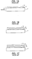
- FIG. 1A illustrates how one starts with a layer of silicon 10 on an insulator 15 and a silicon substrate 11.
- Fig. 1B illustrates that a layer of material, i.e. silicon dioxide 12 is then deposited on the silicon.
- Fig. 1C then shows that a layer of a photoresist 14 material is then deposited on the silicon dioxide. The structure is then irradiated under a binary photomask, the photoresist is developed and excess photoresist material removed.
- a primary objective of the features of the present invention is to provide a fabrication process which avoids the above described disadvantages.
- a surface micromachining process for the fabrication of three-dimensional micro-hinges directly on silicon on insulator wafers comprising the steps of: (a) defining openings around the surface of a desired hinge pin in a single layer of a silicon single crystal; (b) subjecting the openings to an etching process for removal of oxide material that is located in contiguous relation to the openings under the area designated for a hinge; (c) growing thermal oxide to define a gap between a hinge pin and a subsequently deposited polysilicon cap; (d) depositing polysilicon and etching to define a hinge cap/staple; and (e) wet etching to remove grown oxide and allow a pin to rotate inside the cap/staple.
- a connected mirror structure can be lifted out of the silicon wafer.
- the features of the present invention describe a novel method of building micro hinges on top of silicon on insulator (SOI) wafers.
- SOI silicon on insulator
- the method allows fabrication of hinges that can be lifted out of a wafer plane though the method requires only one polysilicon deposition and greatly reduces process complexity and cost.
- the hinges manufactured by this invention are self aligned and have much tighter tolerance than the traditional polysilicon hinges (which typically requires deposition of three polysilicon layers).
- the process according to the present invention also allows the moving plate to be built completely out of single crystal silicon, and significantly reduces the stress and fatigue failure issues associated with polysilicon mirrors.
- the process according to the invention can be extended to traditional surface micro machining to reduce the required number of layers of polysilicon by a deposition technique.
- the application is very broad and can be employed with regard to many movable micro devices, particularly micro optical switches, micro spectral analyzer, micro display, and electric-paper.
- the structure for a typical micro staple hinge 20 is composed of a hinge flap or plate 21 that can rotate as per arrow 22 and a hinge staple 23.
- the flap 21 and staple 23 are connected to separated structures. These are free to rotate relative to each other as per arrow 22.
- Hinges as described herein are typically built by a surface micromachining process.
- the process employed in the prior art is illustrated in Figs. 3 through Fig. 8, wherein a sacrificial layer 30 (silicon oxide) is usually deposited on top of the polysilicon structure 31 that has a hinge post 35 pre-defined (Figs. 3 and 4). Both 31 and 35 are formed of polysilicon (layer 1).
- Layer 34 is a silicon dioxide layer.
- Substrate 32 can be covered by a polysilicon layer 38A and a silicon nitride insulation layer 39A which are both used to prevent charging.
- Anchor holes 36 are etched at both sides of the post 35 through both layers 30 and 34 (Fig. 5), followed by deposition of the polysilicon layer 38. (Fig.
- This polysilicon layer 38 is patterned and etched to form the staple that surrounds the post. At the end of the process, the sacrificial materials are removed by etching (Fig. 7). The remaining polysilicon structures are then allowed to move in the direction of arrow 37 and rotate to fold into the structure. (Fig. 8) If the plate that has the post needs to be moved out of plane, the layer 32 needs to be physically separated from the substrate (Fig. 8).
- a micro hinge device M comprising a substrate 42 which is the basic foundation for the micro-hinge device M. Supported on the substrate 42 is an anchor plate 41, and anchored to anchor plate 41 is staple member 40 which surrounds and holds hinge pin 42A. There is a layer of buried oxide positioned between anchor plate 41 and substrate 42 which layer is needed for electrical insulation.
- “Flap” or "moving plate” or “mirror” 43 can rotate in the direction of arrow 44 out of plane around hinge pin 43A.
- the anchor plate 41, the moving plate 43 and the pin are all made of single crystal silicon.
- the staple 40 is made of polycrystal silicon. All plates are electrically isolated from the substrate 42.
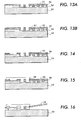
- Figs. 10 through 16 illustrate cross-sectional views of an MEM device during the primary fabrication steps in accordance with the specific process steps defined by the present invention.
- the starting material is an SOI wafer 50 which comprises a single crystal silicon layer 50 having a preferred thickness of about one to about five microns.
- the crystal silicon layer 51 lies over a layer of buried oxide 52 which in turn lies on substrate 53, also a single crystal silicon layer.
- the slots are defined around the hinge pin as shown in Fig. 11 by an etch that forms trenches 54 (slots) into the silicon single crystal layer 51. Thereafter a wet etch is performed to remove the oxide under the hinge pin (Fig. 12).
- thermal oxide layer 56 is grown in the next step (Fig. 13A) to define the gap between the pin and the to-be-deposited polysilicon cap.
- An optional thin layer of CVD oxide (LTO: low temperature oxide) 55 can be deposited immediately afterward to cover fine gaps not completely sealed by the thermal grown oxide in the field, plus to round off the slot opening (Fig. 13B). Because the width of the trench around the pin is larger, the CVD oxide will only round off the top corners, but won't seal off the trench opening.
- the thickness of the thermal oxide layer 56 is about one half the thickness of dimension "d" shown in Fig. 12 and the thickness of layer 55 LTO is less than half of the thickness of layer 56.
- Polysilicon anchor etch is performed in the next step (Fig. 14). Thereafter, polysilicon 59 is deposited (Fig. 15) and etched to define the hinge cap. Since polysilicon has excellent conformality, it will completely fill up the gap underneath the pin and warp around it. This feature allows the hinge 58 to be lifted off the plane completely (Fig. 16). For a direct comparison, it would take at least three (3) polysilicon depositions with traditional surface micro machining techniques to achieve the same functionality. In the last step, the sacrificial oxide is etched away by hydrofluric acid, and the mirror can be lifted out of plane. We can cascade the mirror plates to build lifted platforms.
- Fig. 17 illustrates a hinge system made by the process of the present invention in the form of a chained platform connected by silicon self-aligned micro-hinges made in accordance with the features of the present invention that can be raised in the direction of arrow 64 at any angle.
- the hinge posts are all single crystal silicon as are the various platforms 61 all of which are supported on substrate 62. Fabricated movement will be in the direction of arrow 63, further to the left.
- Platform 61 is typically connected to a micro actuator to push it in the direction of arrow 63, i.e. to the right. When pushed in the direction of arrow 63, the entire structure is raised in the direction of arrow 64 (out of plane). Furthermore, the angle of each plate 61 will be controlled by movement in the direction of arrow 63.
- surface 66 is positioned on platform 61.
- Surface 66 can be a metal reflector, a fine etched grating, for example, or a big hole.
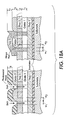
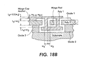
- Fig. 18A is a further illustration of a traditional silicon hinge structure in which three layers of polycrystalline silicon is needed. This is in direct comparison to the self-aligned hinge (SAH) shown in Fig. 18B in accordance with the present invention in which only one layer of polycrystalline silicon is needed for the hinge structure.
- Figs. 18A and 18B illustrate why (how) the tolerances of the self-aligned hinge (Fig. 18B) are better than that of known hinges as illustrated in Fig. 18A.
- the hinge tolerance is defined by the gap between the hinge post (pin) and the cap that surrounds the post.
- the gape is w2 on the side, and t1 and t3 on top and-below.
- the gap is w3, and t4, t5, respectively.
- t1 and t2 are determined by the thickness of oxide 1 and oxide 2. They typically are about 1.5 to 2.5 um.
- W2 is determined by the etching and alignment capability. Basically the w1 etch that is done prior to poly 3 deposition. W1 etch has to go through both oxide 1 and oxide 2 layers, therefore its etch mask must have a reasonable thickness (t6 in Fig. 18A).
- layer-to-layer contact photolithography typically used for building MEMS, has alignment accuracy no better than about 1-1.5 um. Therefore w2 has to be reasonably large enough to prevent accidental lithography alignment error that causes a shift of w1 etch and bridges poly 3 to poly 2 hinge post later on. It is typically about 3 um assuming a 1-1.5 um alignment accuracy.
- w1 has to be wide enough, usually 2-3 times of (t1+t3), and ensure a good etch and proper connection of poly 3 to poly 1 at the end of the process.
- t4 should be approximately equal to t5 and w3 since they are all grown at the same time.
- Thermal oxide is "conformal", meaning its thickness is about equal everywhere.
- W3 should be around 1um or no more than about 1.5 um. It should be just enough to get the hinge to turn. There is no additional lithography/etch steps that need to define the w4 hole, and there is no concern about alignment, mask thickness/step coverage...etc.
- W4 is about 1 ⁇ 2 of t8.
- w2 is usually 3 um
- the width w5 should be about twice of w3, and about 3 um. Spacing w6 will add another 4-5 um.
- Figs. 19 and 20 Scanning electron micrographs of self-aligned micro hinges are shown in Figs. 19 and 20.
- Fig. 19 four hinges connect the right mirror plate to the left.
- the pins are part of the right plate, and the poly caps anchors down to the left mirror plate.
- the sacrificial oxide has been removed and one can see that the poly cap wraps around the single crystal silicon hinge.
- Fig. 19 the right hand side plate rotates up.
- a close-up view of another hinge is also shown in Fig. 20 to better illustrate the tight tolerance of the self-aligned hinges in accordance with the embodiments of the present invention.
Landscapes
- Engineering & Computer Science (AREA)
- Manufacturing & Machinery (AREA)
- Microelectronics & Electronic Packaging (AREA)
- Mechanical Engineering (AREA)
- Micromachines (AREA)
- Pressure Sensors (AREA)
- Mechanical Light Control Or Optical Switches (AREA)
Abstract
Description
Claims (6)
- A surface micromachining process for the fabrication of three-dimensional micro-hinges directly on silicon on insulator wafers (50) comprising the steps of:(a) defining openings (54) around the surface of a desired hinge pin in a single layer (51) of a silicon single crystal;(b) subjecting the openings (54) to an etching process for removal of oxide material (52) that is located in contiguous relation to the openings under the area designated for a hinge;(c) growing thermal oxide (56) to define a gap around the hinge pin;(d) depositing polysilicon (59) and etching to define a hinge cap/staple (59); and(e) wet etching to remove grown oxide (56) and allow relative rotation between the hinge pin and the cap/staple (59).
- A surface micromachining process according to claim 1, wherein after step (c), immediately depositing a thin layer of a chemical vapor deposited oxide (55) sufficient to cover fine gaps not completely covered by said thermal oxide (56).
- A surface micromachining process according to claim 1 or 2, further comprising the step of lifting a structure (58) out of the plane of the silicon wafer (50).
- A surface micromachining process according to claim 3, wherein said structure (58) is a mirror or a grating.
- A surface micromachining process according to any one of the preceding claims, wherein said etching processes are dry etching processes.
- A surface micromachining process according to any one of the preceding claims, wherein said silicon single crystal layer (51) is from about one to about five microns thick.
Applications Claiming Priority (2)
| Application Number | Priority Date | Filing Date | Title |
|---|---|---|---|
| US40687 | 1979-05-21 | ||
| US10/040,687 US6755982B2 (en) | 2002-01-07 | 2002-01-07 | Self-aligned micro hinges |
Publications (3)
| Publication Number | Publication Date |
|---|---|
| EP1325885A2 true EP1325885A2 (en) | 2003-07-09 |
| EP1325885A3 EP1325885A3 (en) | 2004-12-08 |
| EP1325885B1 EP1325885B1 (en) | 2009-04-22 |
Family
ID=21912371
Family Applications (1)
| Application Number | Title | Priority Date | Filing Date |
|---|---|---|---|
| EP03250010A Expired - Lifetime EP1325885B1 (en) | 2002-01-07 | 2003-01-02 | Self-aligned micro hinges |
Country Status (4)
| Country | Link |
|---|---|
| US (1) | US6755982B2 (en) |
| EP (1) | EP1325885B1 (en) |
| JP (1) | JP4313576B2 (en) |
| DE (1) | DE60327274D1 (en) |
Cited By (3)
| Publication number | Priority date | Publication date | Assignee | Title |
|---|---|---|---|---|
| WO2005092782A1 (en) * | 2004-03-02 | 2005-10-06 | Analog Devices, Inc. | Single crystal silicon sensor with additional layer and method of producing the same |
| EP1650158A1 (en) * | 2004-10-20 | 2006-04-26 | Samsung Electronics Co., Ltd. | Silicon-on-insulator substrate, its fabrication method and MEMS floating structure formed therein |
| WO2006110304A1 (en) * | 2005-03-29 | 2006-10-19 | Intel Corporation | Mems drives adapted to provide three degrees of mobility |
Families Citing this family (12)
| Publication number | Priority date | Publication date | Assignee | Title |
|---|---|---|---|---|
| US6952042B2 (en) * | 2002-06-17 | 2005-10-04 | Honeywell International, Inc. | Microelectromechanical device with integrated conductive shield |
| US7067892B1 (en) * | 2002-10-17 | 2006-06-27 | The United States Of America As Represented By The Secretary Of The Air Force | Off substrate flip-chip apparatus |
| US20090113889A1 (en) * | 2006-02-28 | 2009-05-07 | Subir Roychoudhury | Catalytic burner for stirling engine |
| JP2008080444A (en) * | 2006-09-27 | 2008-04-10 | Toshiba Corp | MEMS device manufacturing method and MEMS device |
| US20080208197A1 (en) * | 2006-11-30 | 2008-08-28 | Kelly Ammann | Method and apparatus for performing an open wedge, high tibial osteotomy |
| JP2009291293A (en) | 2008-06-03 | 2009-12-17 | Olympus Corp | Stacked structure, light controlling apparatus, and method of manufacturing stacked structure |
| US20110062110A1 (en) * | 2009-09-16 | 2011-03-17 | Karthik Kumar | Method for Fabricating a Micromirror with Self-Aligned Actuators |
| EP2312393A1 (en) * | 2009-10-14 | 2011-04-20 | Biocartis SA | Method for producing microparticles |
| CN102234098B (en) * | 2010-04-21 | 2014-02-26 | 汉积科技股份有限公司 | Manufacturing method of micro electromechanical structure |
| CN102259820B (en) * | 2010-05-27 | 2013-12-18 | 上海华虹Nec电子有限公司 | Cavity structure, manufacturing method of cavity structure and manufacturing method of pressure-sensitive sensor |
| CN102303843B (en) * | 2011-08-15 | 2014-07-16 | 中国科学技术大学 | Nano fluid channel and manufacturing method thereof |
| CN102320558B (en) * | 2011-09-13 | 2014-03-26 | 上海先进半导体制造股份有限公司 | Manufacturing method for cavity of full silica-based microfluidic device |
Family Cites Families (8)
| Publication number | Priority date | Publication date | Assignee | Title |
|---|---|---|---|---|
| US5177661A (en) * | 1989-01-13 | 1993-01-05 | Kopin Corporation | SOI diaphgram sensor |
| US5488862A (en) * | 1993-10-18 | 1996-02-06 | Armand P. Neukermans | Monolithic silicon rate-gyro with integrated sensors |
| US5759870A (en) * | 1995-08-28 | 1998-06-02 | Bei Electronics, Inc. | Method of making a surface micro-machined silicon pressure sensor |
| US5867297A (en) * | 1997-02-07 | 1999-02-02 | The Regents Of The University Of California | Apparatus and method for optical scanning with an oscillatory microelectromechanical system |
| US6002507A (en) * | 1998-12-01 | 1999-12-14 | Xerox Corpoation | Method and apparatus for an integrated laser beam scanner |
| US6586841B1 (en) * | 2000-02-23 | 2003-07-01 | Onix Microsystems, Inc. | Mechanical landing pad formed on the underside of a MEMS device |
| US6300156B1 (en) * | 2000-04-07 | 2001-10-09 | Agere Systems Optoelectronics Guardian Corp. | Process for fabricating micromechanical devices |
| US6479311B1 (en) * | 2000-11-27 | 2002-11-12 | Microscan Systems, Inc. | Process for manufacturing micromechanical and microoptomechanical structures with pre-applied patterning |
-
2002
- 2002-01-07 US US10/040,687 patent/US6755982B2/en not_active Expired - Fee Related
-
2003
- 2003-01-02 DE DE60327274T patent/DE60327274D1/en not_active Expired - Lifetime
- 2003-01-02 EP EP03250010A patent/EP1325885B1/en not_active Expired - Lifetime
- 2003-01-06 JP JP2003000125A patent/JP4313576B2/en not_active Expired - Fee Related
Cited By (7)
| Publication number | Priority date | Publication date | Assignee | Title |
|---|---|---|---|---|
| WO2005092782A1 (en) * | 2004-03-02 | 2005-10-06 | Analog Devices, Inc. | Single crystal silicon sensor with additional layer and method of producing the same |
| US7138694B2 (en) | 2004-03-02 | 2006-11-21 | Analog Devices, Inc. | Single crystal silicon sensor with additional layer and method of producing the same |
| US8227876B2 (en) | 2004-03-02 | 2012-07-24 | Analog Devices, Inc. | Single crystal silicon sensor with additional layer and method of producing the same |
| US8227286B2 (en) | 2004-03-02 | 2012-07-24 | Analog Devices, Inc. | Single crystal silicon sensor with additional layer and method of producing the same |
| EP1650158A1 (en) * | 2004-10-20 | 2006-04-26 | Samsung Electronics Co., Ltd. | Silicon-on-insulator substrate, its fabrication method and MEMS floating structure formed therein |
| WO2006110304A1 (en) * | 2005-03-29 | 2006-10-19 | Intel Corporation | Mems drives adapted to provide three degrees of mobility |
| US7180650B2 (en) | 2005-03-29 | 2007-02-20 | Intel Corporation | Electromechanical drives adapted to provide three degrees of mobility |
Also Published As
| Publication number | Publication date |
|---|---|
| US20030129374A1 (en) | 2003-07-10 |
| JP2003260699A (en) | 2003-09-16 |
| US6755982B2 (en) | 2004-06-29 |
| DE60327274D1 (en) | 2009-06-04 |
| EP1325885B1 (en) | 2009-04-22 |
| EP1325885A3 (en) | 2004-12-08 |
| JP4313576B2 (en) | 2009-08-12 |
Similar Documents
| Publication | Publication Date | Title |
|---|---|---|
| EP1325885B1 (en) | Self-aligned micro hinges | |
| US6121552A (en) | Microfabricated high aspect ratio device with an electrical isolation trench | |
| US5198390A (en) | RIE process for fabricating submicron, silicon electromechanical structures | |
| US6082208A (en) | Method for fabricating five-level microelectromechanical structures and microelectromechanical transmission formed | |
| US6020272A (en) | Method for forming suspended micromechanical structures | |
| US7898046B2 (en) | Microelectromechanical systems encapsulation process | |
| US7026184B2 (en) | Method of fabricating microstructures and devices made therefrom | |
| US7045466B2 (en) | Three dimensional high aspect ratio micromachining | |
| US20020127760A1 (en) | Method and apparatus for micro electro-mechanical systems and their manufacture | |
| US6887391B1 (en) | Fabrication and controlled release of structures using etch-stop trenches | |
| US20020118850A1 (en) | Micromachine directional microphone and associated method | |
| KR100373739B1 (en) | Method for Fabrication of Electrostatic Vertical Actuators Using One Single-crystalline Silicon Wafer | |
| EP1201602B1 (en) | Thermal out-of-plane buckle-beam actuator | |
| US6328903B1 (en) | Surface-micromachined chain for use in microelectromechanical structures | |
| EP1331201B1 (en) | Structure with thermal out-of-plane buckle-beam acuator | |
| Comtois et al. | Design techniques for surface-micromachining MEMS processes | |
| WO2012112452A2 (en) | Strengthened micro-electromechanical system devices and methods of making thereof | |
| EP1211726B1 (en) | Single-crystal-silicon flexible ribbon for micro-mirror and MEMS assembly on silicon-on-insulator (SOI) material | |
| US5439552A (en) | Process of fabricating an enlongated microstructure element on a substrate | |
| KR100817813B1 (en) | A method for fabricating a micro structures with multi differential gap on silicon substrate | |
| Hofmann et al. | Monolithic three-dimensional single-crystal silicon microelectromechanical systems | |
| US6429034B1 (en) | Method of making high aspect ratio features during surface micromachining | |
| KR100227787B1 (en) | Method of manufacturing silicon microstructure | |
| US7421924B1 (en) | Apparatus for raising or tilting a micromechanical structure | |
| Fleming et al. | Novel silicon fabrication process for high-aspect-ratio micromachined parts |
Legal Events
| Date | Code | Title | Description |
|---|---|---|---|
| PUAI | Public reference made under article 153(3) epc to a published international application that has entered the european phase |
Free format text: ORIGINAL CODE: 0009012 |
|
| AK | Designated contracting states |
Designated state(s): AT BE BG CH CY CZ DE DK EE ES FI FR GB GR HU IE IT LI LU MC NL PT SE SI SK TR |
|
| AX | Request for extension of the european patent |
Extension state: AL LT LV MK RO |
|
| RIN1 | Information on inventor provided before grant (corrected) |
Inventor name: LIN, CHUANG-CHIA |
|
| PUAL | Search report despatched |
Free format text: ORIGINAL CODE: 0009013 |
|
| AK | Designated contracting states |
Kind code of ref document: A3 Designated state(s): AT BE BG CH CY CZ DE DK EE ES FI FR GB GR HU IE IT LI LU MC NL PT SE SI SK TR |
|
| AX | Request for extension of the european patent |
Extension state: AL LT LV MK RO |
|
| 17P | Request for examination filed |
Effective date: 20050608 |
|
| AKX | Designation fees paid |
Designated state(s): DE FR GB |
|
| GRAP | Despatch of communication of intention to grant a patent |
Free format text: ORIGINAL CODE: EPIDOSNIGR1 |
|
| GRAS | Grant fee paid |
Free format text: ORIGINAL CODE: EPIDOSNIGR3 |
|
| GRAA | (expected) grant |
Free format text: ORIGINAL CODE: 0009210 |
|
| AK | Designated contracting states |
Kind code of ref document: B1 Designated state(s): DE FR GB |
|
| REG | Reference to a national code |
Ref country code: GB Ref legal event code: FG4D |
|
| REF | Corresponds to: |
Ref document number: 60327274 Country of ref document: DE Date of ref document: 20090604 Kind code of ref document: P |
|
| PLBE | No opposition filed within time limit |
Free format text: ORIGINAL CODE: 0009261 |
|
| STAA | Information on the status of an ep patent application or granted ep patent |
Free format text: STATUS: NO OPPOSITION FILED WITHIN TIME LIMIT |
|
| 26N | No opposition filed |
Effective date: 20100125 |
|
| REG | Reference to a national code |
Ref country code: FR Ref legal event code: PLFP Year of fee payment: 13 |
|
| PGFP | Annual fee paid to national office [announced via postgrant information from national office to epo] |
Ref country code: GB Payment date: 20141219 Year of fee payment: 13 |
|
| PGFP | Annual fee paid to national office [announced via postgrant information from national office to epo] |
Ref country code: DE Payment date: 20141218 Year of fee payment: 13 |
|
| PGFP | Annual fee paid to national office [announced via postgrant information from national office to epo] |
Ref country code: FR Payment date: 20150121 Year of fee payment: 13 |
|
| REG | Reference to a national code |
Ref country code: DE Ref legal event code: R119 Ref document number: 60327274 Country of ref document: DE |
|
| GBPC | Gb: european patent ceased through non-payment of renewal fee |
Effective date: 20160102 |
|
| REG | Reference to a national code |
Ref country code: FR Ref legal event code: ST Effective date: 20160930 |
|
| PG25 | Lapsed in a contracting state [announced via postgrant information from national office to epo] |
Ref country code: DE Free format text: LAPSE BECAUSE OF NON-PAYMENT OF DUE FEES Effective date: 20160802 Ref country code: GB Free format text: LAPSE BECAUSE OF NON-PAYMENT OF DUE FEES Effective date: 20160102 |
|
| PG25 | Lapsed in a contracting state [announced via postgrant information from national office to epo] |
Ref country code: FR Free format text: LAPSE BECAUSE OF NON-PAYMENT OF DUE FEES Effective date: 20160201 |