EP1324490A2 - Surface acoustic wave device - Google Patents
Surface acoustic wave device Download PDFInfo
- Publication number
- EP1324490A2 EP1324490A2 EP02293237A EP02293237A EP1324490A2 EP 1324490 A2 EP1324490 A2 EP 1324490A2 EP 02293237 A EP02293237 A EP 02293237A EP 02293237 A EP02293237 A EP 02293237A EP 1324490 A2 EP1324490 A2 EP 1324490A2
- Authority
- EP
- European Patent Office
- Prior art keywords
- acoustic wave
- surface acoustic
- signal terminal
- piezoelectric substrate
- line
- Prior art date
- Legal status (The legal status is an assumption and is not a legal conclusion. Google has not performed a legal analysis and makes no representation as to the accuracy of the status listed.)
- Granted
Links
- 238000010897 surface acoustic wave method Methods 0.000 title claims abstract description 100
- 239000000758 substrate Substances 0.000 claims abstract description 54
- 230000005540 biological transmission Effects 0.000 claims description 7
- 239000011295 pitch Substances 0.000 description 8
- 230000010363 phase shift Effects 0.000 description 7
- 230000003111 delayed effect Effects 0.000 description 5
- 230000000694 effects Effects 0.000 description 5
- 238000004904 shortening Methods 0.000 description 5
- 230000008901 benefit Effects 0.000 description 4
- 238000000034 method Methods 0.000 description 4
- 229910012463 LiTaO3 Inorganic materials 0.000 description 3
- 230000006866 deterioration Effects 0.000 description 3
- 238000000206 photolithography Methods 0.000 description 3
- 229910003327 LiNbO3 Inorganic materials 0.000 description 2
- 238000005452 bending Methods 0.000 description 2
- 238000010168 coupling process Methods 0.000 description 2
- 238000005859 coupling reaction Methods 0.000 description 2
- 238000004519 manufacturing process Methods 0.000 description 2
- 239000000463 material Substances 0.000 description 2
- 230000008569 process Effects 0.000 description 2
- 239000000919 ceramic Substances 0.000 description 1
- 238000006243 chemical reaction Methods 0.000 description 1
- 230000006835 compression Effects 0.000 description 1
- 238000007906 compression Methods 0.000 description 1
- 230000008878 coupling Effects 0.000 description 1
- 239000013078 crystal Substances 0.000 description 1
- PCHJSUWPFVWCPO-UHFFFAOYSA-N gold Chemical compound [Au] PCHJSUWPFVWCPO-UHFFFAOYSA-N 0.000 description 1
- 239000010931 gold Substances 0.000 description 1
- 229910052737 gold Inorganic materials 0.000 description 1
- 230000006872 improvement Effects 0.000 description 1
- 230000004048 modification Effects 0.000 description 1
- 238000012986 modification Methods 0.000 description 1
- 230000003071 parasitic effect Effects 0.000 description 1
Images



Classifications
-
- H—ELECTRICITY
- H03—ELECTRONIC CIRCUITRY
- H03H—IMPEDANCE NETWORKS, e.g. RESONANT CIRCUITS; RESONATORS
- H03H9/00—Networks comprising electromechanical or electro-acoustic elements; Electromechanical resonators
- H03H9/25—Constructional features of resonators using surface acoustic waves
-
- H—ELECTRICITY
- H03—ELECTRONIC CIRCUITRY
- H03H—IMPEDANCE NETWORKS, e.g. RESONANT CIRCUITS; RESONATORS
- H03H9/00—Networks comprising electromechanical or electro-acoustic elements; Electromechanical resonators
- H03H9/0023—Networks for transforming balanced signals into unbalanced signals and vice versa, e.g. baluns, or networks having balanced input and output
- H03H9/0028—Networks for transforming balanced signals into unbalanced signals and vice versa, e.g. baluns, or networks having balanced input and output using surface acoustic wave devices
- H03H9/0047—Networks for transforming balanced signals into unbalanced signals and vice versa, e.g. baluns, or networks having balanced input and output using surface acoustic wave devices having two acoustic tracks
- H03H9/0066—Networks for transforming balanced signals into unbalanced signals and vice versa, e.g. baluns, or networks having balanced input and output using surface acoustic wave devices having two acoustic tracks being electrically parallel
- H03H9/0071—Networks for transforming balanced signals into unbalanced signals and vice versa, e.g. baluns, or networks having balanced input and output using surface acoustic wave devices having two acoustic tracks being electrically parallel the balanced terminals being on the same side of the tracks
-
- H—ELECTRICITY
- H03—ELECTRONIC CIRCUITRY
- H03H—IMPEDANCE NETWORKS, e.g. RESONANT CIRCUITS; RESONATORS
- H03H9/00—Networks comprising electromechanical or electro-acoustic elements; Electromechanical resonators
- H03H9/0023—Networks for transforming balanced signals into unbalanced signals and vice versa, e.g. baluns, or networks having balanced input and output
- H03H9/0028—Networks for transforming balanced signals into unbalanced signals and vice versa, e.g. baluns, or networks having balanced input and output using surface acoustic wave devices
- H03H9/0085—Networks for transforming balanced signals into unbalanced signals and vice versa, e.g. baluns, or networks having balanced input and output using surface acoustic wave devices having four acoustic tracks
-
- H—ELECTRICITY
- H03—ELECTRONIC CIRCUITRY
- H03H—IMPEDANCE NETWORKS, e.g. RESONANT CIRCUITS; RESONATORS
- H03H9/00—Networks comprising electromechanical or electro-acoustic elements; Electromechanical resonators
- H03H9/02—Details
- H03H9/125—Driving means, e.g. electrodes, coils
- H03H9/145—Driving means, e.g. electrodes, coils for networks using surface acoustic waves
- H03H9/14544—Transducers of particular shape or position
- H03H9/14576—Transducers whereby only the last fingers have different characteristics with respect to the other fingers, e.g. different shape, thickness or material, split finger
- H03H9/14582—Transducers whereby only the last fingers have different characteristics with respect to the other fingers, e.g. different shape, thickness or material, split finger the last fingers having a different pitch
Definitions
- the present invention relates to a surface acoustic wave device for use as a band-pass filter, and more particularly to a surface acoustic wave device of which one of the input terminal and the output terminal is an unbalanced signal terminal.
- the difference between the amplitudes at a pair of terminals provided on the balanced side (hereinafter, referred to as an amplitude balance characteristic) is required to be zero, and the difference between the phases (hereinafter, referred to as a phase balance characteristic) also is required to be about 180°.
- Fig. 6 is a schematic view of an example of a related art surface acoustic wave device having a balanced-to-unbalanced function.
- longitudinal-coupling resonator type SAW filters 201 and 202, and 1 port type SAW resonators 203 and 204 are composed of Al electrodes on a piezoelectric substrate.
- the input sides of the SAW filters 201 and 202 are connected in parallel to each other and also are connected to an unbalanced signal terminal 205.
- the output sides of the SAW filters 201 and 202 are connected in series with the SAW resonators 203 and 204, respectively.
- the SAW resonators 203 and 204 are connected to balanced signal terminals 206 and 207, respectively.
- IDTs 201a and 201b which are positioned on the unbalanced sides and are adjacent to reflectors have inverted-shapes with respect to IDTs 202a and 202b which are adjacent to the reflectors in the SAW filter 202.
- a signal output from the balanced signal terminal 206 and the signal output from the balanced signal terminal 207 have a phase difference of 180°.
- the electrode fingers 201d and 201e which are adjacent to the center IDT 201c are connected to the unbalanced signal terminal 205, respectively.
- the electrode fingers 202d and 202e which are adjacent to the center IDT 202c are connected to the ground potential, respectively. Accordingly, the phase characteristic of the SAW filter 202 is not exactly equal to the inverted characteristic obtained when the phase of the SAW filter 201 is inverted by 180°. Thus, the phase balance characteristic of the surface acoustic wave 200 device can not avoid departing from 180° (the ideal value).
- the layout thereof such as a wiring structure ranging from a unbalanced signal terminal to a pair of balanced signal terminals is not symmetrical with respect to the unbalanced signal terminal.
- the parasitic capacitances of the lines extending to a pair of the balanced signal terminals become different. This readily causes deterioration of the phase balance characteristic.
- a surface acoustic wave device which comprises: a piezoelectric substrate; at least one interdigital transducer (IDT) arranged on the piezoelectric substrate; an input terminal and an output terminal, one of the input terminal and the output terminal comprising an unbalanced signal terminal, the other terminal comprising first and second balanced signal terminals; and a delay line provided on the unbalanced signal terminal side in the path between the unbalanced signal terminal and the first balanced signal terminal. Accordingly, the phase of a signal in the line in which the delay line is introduced is delayed, due to the introduction of the delay line. Thus, the phase balance characteristic is improved.
- the surface acoustic wave device having a balanced-to-unbalanced function with a superior phase balance characteristic can be provided.
- the delay line is formed on the piezoelectric substrate.
- the surface acoustic wave device can be easily designed compared to the case where the delay line is formed on the package side.
- the delay line can be formed easily at high precision on the piezoelectric substrate using a photolithography technique.
- the design of the delay line can be easily changed.
- a surface acoustic wave device which comprises: a first surface acoustic wave filter element including a piezoelectric substrate, and at least two interdigital transducers (IDTs) arranged along the surface acoustic wave propagation direction on the piezoelectric substrate; a second surface acoustic wave filter element including a piezoelectric substrate, and at least two interdigital transducers (IDTs) arranged along the surface acoustic wave propagation direction on the piezoelectric substrate, the second surface acoustic wave filter element having a transmission phase characteristic different by about 180° from that of the first surface acoustic wave filter element; the first and second surface acoustic wave filter elements each having an input terminal and an output terminal, ones of the input terminals and the output terminals of the first and second surface acoustic wave filter elements being commonly connected to each other at a common connection point; an unbalanced signal terminal being connected to the common connection point
- the delay line is formed on the piezoelectric substrate.
- the surface acoustic wave device can be easily designed compared to the case where the delay line is formed on the package side. The cost can be reduced.
- the delay line can be formed easily at high precision on the piezoelectric substrate using a photolithography technique.
- the design of the delay line can be easily changed.
- the length of the signal line between the common connection point and the IDTs of the first surface acoustic wave filter element electrically connected to the common connection point is different from the length of the signal line between the common connection point and the IDTs of the second surface acoustic wave filter element electrically connected to the common connection point.
- This line length difference forms the delay line.
- the device is configured so that the phases of input-output signals in the line between the unbalanced signal terminal and the first balanced signal terminal and, those of the input-output signals in the line between the unbalanced signal terminal and the second balanced signal terminal are different by 0.5° to 4° from each other, due to the delay line.
- the surface acoustic wave device contains a second delay line which is connected to the first balanced signal terminal and is formed on the piezoelectric substrate.
- the delay lines are arranged in a dispersed manner, and thereby, the phase balance characteristic can be more effectively improved.
- the length of each delay line can be reduced, and the delay lines can be easily arranged.
- the device is configured so that the phases of input-output signals in the line between the unbalanced signal terminal and the first balanced signal terminal and, those of the input-output signals in the line between the unbalanced signal terminal and the second balanced signal terminal are different by 0.5° to 4° from each other, due to the above-described delay line and the second delay line.
- the phase balance characteristic of the surface acoustic wave device can be effectively improved, and moreover, the size can be further reduced, while deterioration of other characteristics can be suppressed.
- a surface acoustic wave device comprising: a first surface acoustic wave filter element including a piezoelectric substrate, and at least two interdigital transducers (IDTs) arranged along the surface acoustic wave propagation direction on the piezoelectric substrate; a second surface acoustic wave filter element including a piezoelectric substrate, and at least two interdigital transducers (IDTs) arranged along the surface acoustic wave propagation direction on the piezoelectric substrate, the second surface acoustic wave filter element having a transmission phase characteristic different by about 180° from that of the first surface acoustic wave filter element; the first and second surface acoustic wave filter elements each having an input terminal and an output terminal, ones of the input terminals and the output terminals of the first and second surface acoustic wave filter elements being commonly connected to each other at a common connection point; an unbalanced signal terminal being connected to the common connection point
- the first length of the signal line between the common connection point and the interdigital transducers of the first surface acoustic wave filter element electrically connected to the common connection point and the second length of the signal line between the common connection point and the interdigital transducers of the second surface acoustic wave filter element electrically connected to the common connection point are different from each other such that the phases of input-output signals are different from each other to the extent of 0.5° to 4° in the line between the unbalanced signal terminal and the first balanced signal terminal and in the line between the unbalanced signal terminal and the second balanced signal terminal.
- the phase balance characteristic can be more effectively improved, the size can be further reduced, and deterioration of other characteristics can be suppressed.
- the length of the signal line between the unbalanced signal terminal and the first balanced signal terminal and the length of the signal line between the unbalanced signal terminal and the second balanced signal terminal are different from each other, and the difference L (mm) between the line lengths satisfies formula 417/fc ⁇ L ⁇ 3330/fc in which fc represents the center frequency (MHz). Also, in this case, the phase balance characteristic of the surface acoustic wave device can be more effectively improved.
- Fig. 1 is a schematic plan view of a surface acoustic wave device according to a first embodiment of the present invention.
- the electrode structure shown in Fig. 1 is formed on a piezoelectric substrate using Al electrodes.
- a 40 ⁇ 5° Y cut X propagation LiTaO 3 substrate is used as the piezoelectric substrate.
- the piezoelectric material for the piezoelectric substrate is not restricted to the above-described material.
- LiTaO 3 substrates having other cut angles, piezoelectric single crystal substrates of 64° to 72° Y cut X propagation LiNbO 3 and 41° Y cut X propagation LiNbO 3 , and piezoelectric ceramic substrates may be employed.
- First and second longitudinal coupling type resonator type SAW filters 101 and 102 and 1 port type SAW resonator 103 and 104 are formed on the piezoelectric substrate.
- IDTs 105 to 107 are arranged in the surface acoustic wave propagation direction.
- Reflectors 108 and 109 are arranged on the opposite sides, in the surface acoustic wave propagation direction, of the region of the piezoelectric substrate where the IDTs 105 to 107 are formed, respectively.
- the pitches of at least two electrode fingers of the IDTs 105 and 106 facing the gap between the IDTs 105 and 106 and at least two electrode fingers of IDTs 106 and 107 facing the gap between the IDTs 106 and 107 are set to be smaller than the pitches of the other electrode fingers, respectively.
- the pitch of at least two electrode fingers arranged in each of the areas A shown in Fig. 1 is set to be smaller than that of the other electrode fingers of the IDTs 105 to 107.
- the SAW filter 102 is configured in a way similar to that for the SAW filter 101. However, the direction (the upper-lower side direction of Fig. 1) of the IDTs 105' and 107' of the SAW filter 102 is reverse to that of the IDTs 105 and 107 of the SAW filter 101. In particular, the IDTs 105' and 107' are directed reversely to the IDTs 105 and 107 so that an output signal from the SAW filter 101 has the phase opposite to that of the output signal from the SAW filter 102.
- the SAW resonators 103 and 104 are connected in series with the output terminals of the SAW filters 101 and 102, respectively.
- the SAW filters 101 and 102 are connected to each other at a common connection point 110.
- the common connection point 110 is connected to an unbalanced signal terminal 112 which functions as an input signal terminal.
- first and second balanced signal terminals 113 and 114 as output terminals are connected to the output sides of the SAW resonators 103 and 104, respectively.
- a delay line 117 is incorporated between the input side of the SAW filter 101 and the common connection point 110.
- the delay line 117 is introduced on the unbalanced signal terminal side according to the present invention.
- a second delay line 116 is incorporated between the SAW resonator 103 and the balanced signal terminal 113.
- the delay lines 116 and 117 are formed by bending the signal lines made of Al electrodes, that is, increasing the length of the transmission lines, respectively.
- the term "interval” means the distance between the centers of two electrode fingers.
- the numbers of electrode fingers in the IDTs 105', 106', and 107' are equal to those of the IDTs 105, 106, and 107, respectively.
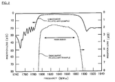
- Figs. 2 to 4 show the characteristics of the surface acoustic wave device configured as described above.
- Figs. 2 to 4 also show the characteristics of the related art surface acoustic wave device designed and shown in Fig. 6 which is the same as that of the above-described embodiment excepting that no delay lines 116 and 117 are provided.
- Fig. 2 shows the frequency - transmission amplitude characteristics
- Fig. 3 shows the frequency - amplitude balance characteristics
- Fig. 4 shows the frequency - phase balance characteristics.
- the broken line represents the characteristics plotted based on a magnified scale on the right side of the graph.
- the broken lines for the related art example and the embodiment of the present invention overlap each other, since the characteristics thereof are substantially coincident with each other.
- Figs. 3 and 4 the characteristics of the embodiment are shown by solid lines, and those of the related art example are illustrated by broken lines.
- the frequency - transmission amplitude characteristics and the frequency - amplitude balance characteristics of the surface acoustic wave devices according to the embodiment and the related art example have substantially no differences.
- the phase balance characteristic in the pass-band of the surface acoustic wave device 100 of the embodiment is considerably improved compared to that of the related art surface acoustic wave device.
- the phase balance characteristic of the related art example has the maximum deviation of 7.2° from 180° near 1865 MHz.
- the maximum deviation near the above-described frequency of the phase balance characteristic of the embodiment is considerably reduced, namely, is 5.8°.
- the phase balance characteristic is shifted in the minus direction from 180°.
- the phase balance characteristic is shifted by about 1.5° in the plus direction from that of the related art characteristic.
- the phase balance characteristic in a large part of the pass-band is shifted in the minus direction from 180°.
- the delay lines 116 and 117 are introduced on the signal line between the unbalanced signal terminal 112 and the balanced signal terminal 113, respectively. Thereby, the phase balance characteristic is shifted in the plus direction.
- the balanced signal terminal 114 is the first balanced signal terminal according to the present invention.
- the difference between the phases of signals output from the SAW filter 101 and from the SAW filter 102, caused by the difference between the configurations of the SAW filters 101 and 102, is adjusted by making different the line length between the unbalanced signal terminal 112 and the balanced signal terminal 113 from that between the unbalanced signal terminal 112 and the balanced signal terminal 114.
- the phase balance characteristic is improved.
- the delay lines 116 and 117 are arranged on the piezoelectric substrate.
- the delay lines 116 and 117 can be formed on a package (not shown) onto which the piezoelectric substrate is mounted.
- a package not shown
- Great labor and cost are required. Even if the mass production becomes possible, the versatility of the package is reduced, and the cost of the package is increased.
- the delay lines 116 and 117 are arranged on the piezoelectric substrate side. Accordingly, the delay lines can be formed easily at high precision by a photolithography process. Moreover, the design of the delay lines can be easily modified.
- the package can be formed so as to be suitable for common use. Thus, the versatility of the package can be enhanced.
- the delay line 116 is incorporated on the balanced signal terminal 113 side, and the delay line 117 is incorporated on the common connection point 110 side.
- the delay time and the shift amount of the phase balance characteristic are determined by the total line length of the delay lines 116 and 117. Accordingly, by providing both of the delay lines 116 and 117, the phase balance characteristic can be more shifted. In other words, a delay line having a required length can be divided into two parts and provided. Accordingly, the line length per one delay line can be reduced.
- the delay lines can be easily arranged in a restricted space on the piezoelectric substrate.
- the delay line 116 is not necessarily provided.
- the delay line 117 on its own may be provided, and thereby, the phase balance characteristic can be considerably improved as described above.
- the surface acoustic wave device 100 is mounted onto a package by a flip-chip process
- bumps made of gold are formed on the portions of the piezoelectric substrate on which the signal terminals 112, 113, and 114 are provided.
- large occupied areas are required for bump-bonding.
- a space in which the delay line 116 is to be arranged can not be secured on the side where the balanced signal terminals 113 and 114 are provided.
- a space in which the delay line 117 is arranged can be taken on the unbalanced signal terminal 112 side.
- the delay line 117 can be easily arranged on the piezoelectric substrate.
- the delay line 117 is provided as a part of the signal line, provided on the piezoelectric substrate, between the common connection point 110 and the IDTs 105 and 107.
- the delay line 117 may be configured in other forms.
- wires may be used between the unbalanced signal terminal 112 and the SAW filters 101 and 102. That is, a first wire may be used so as to connect an electrode pad associated with the unbalanced signal terminal 112 to an electrode pad associated with the IDTs 105 and 107, and a second wire can be used to connect an electrode pad associated with the unbalanced signal terminal 112 to an electrode pad associated with the IDTs 105' and 107'.
- the first wire is longer than the second wire, whereby to add a delay line in the path from the unbalanced signal terminal 112 to the SAW filter 101.
- the signal line pattern provided on the piezoelectric substrate is used to constitute the delay line 117, this time the delay line is not formed by creating a bent portion of the signal line, instead it is provided by shifting the position of the common connection point 110 towards the right compared to the position shown in Fig.1.
- the common connection point 110 is located closer to the SAW filter 102 than to the SAW filter 101.
- the wire connecting the unbalanced signal terminal 112 to the signal line pattern on the piezoelectric substrate connects to the signal line pattern at a location (110) which is closer to the SAW filter 102 than to the SAW filter 101).
- the extra distance between the common connection point 110 and the SAW filter 101 serves as the delay line.
- a surface acoustic wave device having a balanced-to-unbalanced function to which this embodiment is applied is not especially restricted, provided that two SAW filters are commonly connected on the unbalanced signal terminal side. That is, the configuration of the surface acoustic wave device may be one shown in Fig. 1, or may contain a first SAW filter element comprising cascade-type resonator SAW filters 101 and 101A which are connected to each other longitudinally in two steps, and a second SAW filter element comprising cascade-type resonator SAW filters 101' and 101A' which are connected to each other longitudinally in two steps, as shown in Fig. 5. Moreover, needless to say, the SAW resonators 103 and 104 are not necessarily provided in the configuration of Fig.1.
- the design parameters such as the electrode finger meshing width set forth for the surface acoustic wave device 102 of the above-described embodiment may be changed, if necessary. In this case, the advantages of the present invention can be also obtained.
- the advantage with which the phase balance characteristic can be improved by introduction of the delay line on the unbalanced signal terminal side in the signal line between the unbalanced signal terminal and the first balanced signal terminal is based on the fact that the phase of a signal is delayed correspondingly to the length of the delay line. Accordingly, the shift amount of the phase balance characteristic corresponds to the required length of the delay line, that is, the difference between the line length from the unbalanced signal terminal 112 to the balanced signal terminal 113 and the line length from the unbalanced signal terminal 112 to the balanced signal terminal 114.
- phase balance characteristic of the related art example is shifted by about ⁇ 7° from 180° in the pass-band, as seen in the frequency - phase balance characteristic of the related art example shown in Fig. 4. Practically, phase deviations of ⁇ several degrees are present in surface acoustic wave devices having other configurations.
- the phase balance characteristic it is preferred to set the phase shift amount at 0.5° or more.
- the phase balance characteristic can be improved effectively and sufficiently, if the phase shift amount of at least 0.5° is attained.
- the phase balance characteristic is not shifted in a constant direction from the phase balance degree of 180° in the pass-band, but toward the plus side or the minus side depending on the frequency.
- the phase balance characteristic is improved almost in the whole frequency range of the pass-band.
- the phase balance characteristic tends to be shifted toward the plus side and deteriorated at about 1800MHz.
- the improvement amount is a maximum of + 1.5°, due to the presence of the above-described frequency region at about 1800MHz.
- the length of the delay line is set in such a manner that the phase shift amount becomes up to 4°. If the phase shift amount is excessively large, a very long line will be required on the piezoelectric substrate. The resistance is increased, and the occupied area also is increased. Accordingly, to improve the phase balance characteristic, avoid increasing of the resistance, and reduce the size according to the present invention, preferably, the phase shift amount is set to be in the range of 0.5° to 4°.
- the propagation speed of an electrical signal is about 3 x 10 8 m/second.
- the length L (mm) of the delay line corresponding to the phase shift range of 0.5° to 4° is 417/fc ⁇ L ⁇ 3330/fc. That is, the present invention is more advantageous, when the delay line having a length in the above-described range is provided.
- the length of the delay line 117 is set at about 700 ⁇ m, and thereby, the phase balance characteristic can be shifted by about 1.6°.
- the lengths of the delay lines 116 and 117 are set to be longer by 350 ⁇ m by bending the signal wirings, respectively.
- the phase balance characteristic can be shifted by about 1.6°.
- the delay lines are ideal microstrip lines
- the wavelength of a propagation signal is reduced to be 1/ ( ⁇ e ) 1/2 times thereof.
- the effective dielectric constant ⁇ e becomes about a half of the permittivity ⁇ r of the piezoelectric substrate, since the thickness of the piezoelectric substrate is sufficiently greater than the strip line width.
- an LiTaO 3 substrate having a permittivity ⁇ r of about 43 is used as the piezoelectric substrate.
- the overall length of the delay lines 116 and 117 is set at 700 ⁇ m, and thereby, the phase balance characteristic is shifted by about 1.6°.
- This result shows that the above-described wavelength shortening effect does not need to be considered.
- the delay lines 116 and 117 have a U-letter shape, as shown in Fig. 1, and also, the ground electrode or signal electrodes are provided around the delay lines, so that the above-described theoretical expression is not effective.
- the length of the delay line can be shortened correspondingly to the wavelength-shortening effect.
- the inventors of the present invention have confirmed that the wavelength-shortening effect exerts substantially no influences when the delay line is provided in a narrow space on the piezoelectric substrate. Accordingly, to improved the phase balance characteristic of the surface acoustic wave device in practice according to the present invention, it is especially effective to provide the delay line of which the length L is in range of 417/fc ⁇ L ⁇ 3330/fc, as described above.
Landscapes
- Physics & Mathematics (AREA)
- Acoustics & Sound (AREA)
- Surface Acoustic Wave Elements And Circuit Networks Thereof (AREA)
Abstract
Description
- The present invention relates to a surface acoustic wave device for use as a band-pass filter, and more particularly to a surface acoustic wave device of which one of the input terminal and the output terminal is an unbalanced signal terminal.
- In recent years, the demand for surface acoustic wave devices for use at the RF stages of portable telephones having a balanced-to-unbalanced function, a so-called balun function, have increased, and their use at the RF stages of GSM system portable telephones has started.
- Regarding the balanced-to-unbalanced function, the difference between the amplitudes at a pair of terminals provided on the balanced side (hereinafter, referred to as an amplitude balance characteristic) is required to be zero, and the difference between the phases (hereinafter, referred to as a phase balance characteristic) also is required to be about 180°.
- Fig. 6 is a schematic view of an example of a related art surface acoustic wave device having a balanced-to-unbalanced function.
- In a surface
acoustic wave device 200 shown in Fig. 6, longitudinal-coupling resonatortype SAW filters type SAW resonators SAW filters unbalanced signal terminal 205. The output sides of theSAW filters SAW resonators SAW resonators balanced signal terminals - In the
SAW filter 201 shown in Fig. 6,IDTs 201a and 201b which are positioned on the unbalanced sides and are adjacent to reflectors have inverted-shapes with respect toIDTs SAW filter 202. Thereby, a signal output from thebalanced signal terminal 206 and the signal output from thebalanced signal terminal 207 have a phase difference of 180°. - According to the configuration shown in Fig. 6, of a plurality of the electrodes of the IDT201a and the IDT201b contained in the
SAW filter 201, theelectrode fingers 201d and 201e which are adjacent to the center IDT 201c are connected to theunbalanced signal terminal 205, respectively. On the other hand, of a plurality of the electrodes of the IDT202a and the IDT202b of theSAW filter 202, theelectrode fingers center IDT 202c are connected to the ground potential, respectively. Accordingly, the phase characteristic of theSAW filter 202 is not exactly equal to the inverted characteristic obtained when the phase of theSAW filter 201 is inverted by 180°. Thus, the phase balance characteristic of the surfaceacoustic wave 200 device can not avoid departing from 180° (the ideal value). - Moreover, in some of the related art surface acoustic wave devices having a balanced-to-unbalanced conversion function, the layout thereof such as a wiring structure ranging from a unbalanced signal terminal to a pair of balanced signal terminals is not symmetrical with respect to the unbalanced signal terminal. In this case, the parasitic capacitances of the lines extending to a pair of the balanced signal terminals become different. This readily causes deterioration of the phase balance characteristic.
- Accordingly, it is an object to the present invention to provide a surface acoustic wave device having a balanced-to-unbalanced function and a superior phase balance characteristic.
- According to a first aspect of the present invention, there is provided a surface acoustic wave device which comprises: a piezoelectric substrate; at least one interdigital transducer (IDT) arranged on the piezoelectric substrate; an input terminal and an output terminal, one of the input terminal and the output terminal comprising an unbalanced signal terminal, the other terminal comprising first and second balanced signal terminals; and a delay line provided on the unbalanced signal terminal side in the path between the unbalanced signal terminal and the first balanced signal terminal. Accordingly, the phase of a signal in the line in which the delay line is introduced is delayed, due to the introduction of the delay line. Thus, the phase balance characteristic is improved. Thus, the surface acoustic wave device having a balanced-to-unbalanced function with a superior phase balance characteristic can be provided.
- Preferably, the delay line is formed on the piezoelectric substrate. In this case, the surface acoustic wave device can be easily designed compared to the case where the delay line is formed on the package side. Moreover, the delay line can be formed easily at high precision on the piezoelectric substrate using a photolithography technique. Moreover, the design of the delay line can be easily changed.
- According to a second aspect of the present invention, there is provided a surface acoustic wave device which comprises: a first surface acoustic wave filter element including a piezoelectric substrate, and at least two interdigital transducers (IDTs) arranged along the surface acoustic wave propagation direction on the piezoelectric substrate; a second surface acoustic wave filter element including a piezoelectric substrate, and at least two interdigital transducers (IDTs) arranged along the surface acoustic wave propagation direction on the piezoelectric substrate, the second surface acoustic wave filter element having a transmission phase characteristic different by about 180° from that of the first surface acoustic wave filter element; the first and second surface acoustic wave filter elements each having an input terminal and an output terminal, ones of the input terminals and the output terminals of the first and second surface acoustic wave filter elements being commonly connected to each other at a common connection point; an unbalanced signal terminal being connected to the common connection point; the other terminals of the input terminals and the output terminals of the first and second surface acoustic wave filter elements being first and second balanced signal terminals, respectively; and a delay line provided between the common connection point and the first surface acoustic wave filter element. Thus, the phase of a signal on the first surface acoustic wave filter element side is delayed compared to the phase of the signal on the other surface acoustic wave filter element side, and hence, the phase balance characteristic is improved.
- Also, preferably, the delay line is formed on the piezoelectric substrate. In this case, the surface acoustic wave device can be easily designed compared to the case where the delay line is formed on the package side. The cost can be reduced. Moreover, the delay line can be formed easily at high precision on the piezoelectric substrate using a photolithography technique. Moreover, the design of the delay line can be easily changed.
- Preferably, the length of the signal line between the common connection point and the IDTs of the first surface acoustic wave filter element electrically connected to the common connection point is different from the length of the signal line between the common connection point and the IDTs of the second surface acoustic wave filter element electrically connected to the common connection point. This line length difference forms the delay line.
- Also, preferably, the device is configured so that the phases of input-output signals in the line between the unbalanced signal terminal and the first balanced signal terminal and, those of the input-output signals in the line between the unbalanced signal terminal and the second balanced signal terminal are different by 0.5° to 4° from each other, due to the delay line.
- Preferably, the surface acoustic wave device contains a second delay line which is connected to the first balanced signal terminal and is formed on the piezoelectric substrate. In this case, the delay lines are arranged in a dispersed manner, and thereby, the phase balance characteristic can be more effectively improved. Moreover, the length of each delay line can be reduced, and the delay lines can be easily arranged.
- Further, preferably, the device is configured so that the phases of input-output signals in the line between the unbalanced signal terminal and the first balanced signal terminal and, those of the input-output signals in the line between the unbalanced signal terminal and the second balanced signal terminal are different by 0.5° to 4° from each other, due to the above-described delay line and the second delay line. Thus, the phase balance characteristic of the surface acoustic wave device can be effectively improved, and moreover, the size can be further reduced, while deterioration of other characteristics can be suppressed.
- The above-described advantages can be obtained in the configuration of the device in which the delay line and the second delay line are formed in such a manner that the phases of an electrical signal are different from each other to the extent of 0.5° to 4°.
- According to a third aspect of the present invention, there is provided a surface acoustic wave device comprising: a first surface acoustic wave filter element including a piezoelectric substrate, and at least two interdigital transducers (IDTs) arranged along the surface acoustic wave propagation direction on the piezoelectric substrate; a second surface acoustic wave filter element including a piezoelectric substrate, and at least two interdigital transducers (IDTs) arranged along the surface acoustic wave propagation direction on the piezoelectric substrate, the second surface acoustic wave filter element having a transmission phase characteristic different by about 180° from that of the first surface acoustic wave filter element; the first and second surface acoustic wave filter elements each having an input terminal and an output terminal, ones of the input terminals and the output terminals of the first and second surface acoustic wave filter elements being commonly connected to each other at a common connection point; an unbalanced signal terminal being connected to the common connection point; and the other terminals of the input terminals and the output terminals of the first and second surface acoustic wave filter elements being first and second balanced signal terminals, respectively, wherein a first length of the signal line between the common connection point and the interdigital transducers of the first surface acoustic wave filter element electrically connected to the common connection point is different from a second length of the signal line between the common connection point and the interdigital transducers of the second surface acoustic wave filter element electrically connected to the common connection point. Accordingly, the phase of one of the first and second surface acoustic wave filter elements is delayed compared to that of the other surface acoustic wave filter element, and thereby, the phase balance characteristic can be improved.
- Preferably, the first length of the signal line between the common connection point and the interdigital transducers of the first surface acoustic wave filter element electrically connected to the common connection point and the second length of the signal line between the common connection point and the interdigital transducers of the second surface acoustic wave filter element electrically connected to the common connection point are different from each other such that the phases of input-output signals are different from each other to the extent of 0.5° to 4° in the line between the unbalanced signal terminal and the first balanced signal terminal and in the line between the unbalanced signal terminal and the second balanced signal terminal. In this case, the phase balance characteristic can be more effectively improved, the size can be further reduced, and deterioration of other characteristics can be suppressed.
- Preferably, on the piezoelectric substrate, the length of the signal line between the unbalanced signal terminal and the first balanced signal terminal and the length of the signal line between the unbalanced signal terminal and the second balanced signal terminal are different from each other, and the difference L (mm) between the line lengths satisfies formula 417/fc < L < 3330/fc in which fc represents the center frequency (MHz). Also, in this case, the phase balance characteristic of the surface acoustic wave device can be more effectively improved.
-
- Fig. 1 is a schematic plan view of a surface acoustic wave device according to an embodiment of the present invention;
- Fig. 2 is a graph showing the transmission characteristics of the surface acoustic wave devices according to the embodiment and the related art;
- Fig. 3 is a graph showing the amplitude balance characteristics of the surface acoustic wave devices according to the embodiment and the related art;
- Fig. 4 is a graph showing the phase balance characteristics of the surface acoustic wave devices according to the embodiment and the related art;
- Fig. 5 is a schematic plan view of a modification of the surface acoustic wave device of the present invention, and
- Fig. 6 is a schematic plan view of an example of the related art surface acoustic wave device.
-
- Hereinafter, further features and advantages of the present invention will be more apparent from the following description of preferred embodiments thereof, given by way of example, made with reference to the accompanying drawings.
- Fig. 1 is a schematic plan view of a surface acoustic wave device according to a first embodiment of the present invention.
- According to the first embodiment, the electrode structure shown in Fig. 1 is formed on a piezoelectric substrate using Al electrodes. A 40±5° Y cut X propagation LiTaO3 substrate is used as the piezoelectric substrate. The piezoelectric material for the piezoelectric substrate is not restricted to the above-described material. LiTaO3 substrates having other cut angles, piezoelectric single crystal substrates of 64° to 72° Y cut X propagation LiNbO3 and 41° Y cut X propagation LiNbO3, and piezoelectric ceramic substrates may be employed.
- First and second longitudinal coupling type resonator type SAW filters 101 and 102 and 1 port
type SAW resonator - In the
SAW filter 101,IDTs 105 to 107 are arranged in the surface acoustic wave propagation direction.Reflectors IDTs 105 to 107 are formed, respectively. - The pitches of at least two electrode fingers of the
IDTs IDTs IDTs IDTs IDTs 105 to 107. - The
SAW filter 102 is configured in a way similar to that for theSAW filter 101. However, the direction (the upper-lower side direction of Fig. 1) of the IDTs 105' and 107' of theSAW filter 102 is reverse to that of theIDTs SAW filter 101. In particular, the IDTs 105' and 107' are directed reversely to theIDTs SAW filter 101 has the phase opposite to that of the output signal from theSAW filter 102. - The
SAW resonators - In the surface
acoustic wave device 100, the SAW filters 101 and 102 are connected to each other at acommon connection point 110. Thecommon connection point 110 is connected to anunbalanced signal terminal 112 which functions as an input signal terminal. - On the other hand, first and second
balanced signal terminals SAW resonators - Furthermore, a
delay line 117 is incorporated between the input side of theSAW filter 101 and thecommon connection point 110. Thedelay line 117 is introduced on the unbalanced signal terminal side according to the present invention. Moreover, asecond delay line 116 is incorporated between theSAW resonator 103 and thebalanced signal terminal 113. - The
delay lines - Specific designs for the surface acoustic wave device of this embodiment will be described below. It is to be noted that in the following description, the term "interval" means the distance between the centers of two electrode fingers.
the finger overlap of electrode fingers inSAW filters
the number of IDT electrode fingers inSAW filters
22 electrode fingers in IDT 105 (of the 22 electrode fingers, 3 electrode fingers exist in the above-described narrow pitch region, A),
33 electrode fingers in IDT 106 (of the 33 electrode fingers, 3 electrode fingers exist in each of the narrow pitch regions arranged at both ends, in the surface acoustic wave propagation direction, ofIDT 106, and
22 electrode fingers in IDT 107 (of the 22 electrode fingers, 3 electrode fingers exist in the above-described narrow pitch region) - The numbers of electrode fingers in the IDTs 105', 106', and 107' are equal to those of the
IDTs
the numbers of electrode fingers in each of thereflectors
the wavelength λI inIDTs 105 to 107 and 105' to 107'; 2.1422 µm
the wavelength in the narrow pitch regions of the IDTs is 1.9295 µm
the wavelength λR in a reflector; 2.1770 µm
the IDT to IDT interval in the SAW filters 101 and 102; 0.4432λR
the IDT to reflector interval in the SAW filters 101 and 102; 0.496λR
the IDT electrode finger width/pitch in the SAW filters 101 and 102 (duty ratio); 0.63
the electrode finger meshing width in theSAW resonators
the IDT number in theSAW resonators
the number of electrode fingers in a reflector of each of theSAW resonator
the wavelengths in IDT and reflector of theSAW resonators
the line length ofdelay line 116; 350 µm
the line length ofdelay line 117; 350 µm - Figs. 2 to 4 show the characteristics of the surface acoustic wave device configured as described above. For comparison, Figs. 2 to 4 also show the characteristics of the related art surface acoustic wave device designed and shown in Fig. 6 which is the same as that of the above-described embodiment excepting that no
delay lines - As seen in Figs. 2 and 3, the frequency - transmission amplitude characteristics and the frequency - amplitude balance characteristics of the surface acoustic wave devices according to the embodiment and the related art example have substantially no differences.
- On the other hand, as seen in Fig. 4, the phase balance characteristic in the pass-band of the surface
acoustic wave device 100 of the embodiment is considerably improved compared to that of the related art surface acoustic wave device. In particular, the phase balance characteristic of the related art example has the maximum deviation of 7.2° from 180° near 1865 MHz. On the other hand, the maximum deviation near the above-described frequency of the phase balance characteristic of the embodiment is considerably reduced, namely, is 5.8°. - In the related art example, the phase balance characteristic is shifted in the minus direction from 180°. For the embodiment of the present invention, the phase balance characteristic is shifted by about 1.5° in the plus direction from that of the related art characteristic. Thus, a superior phase balance characteristic in the pass-band is attained. This is due to the fact that the phase of a signal output from the first
balanced signal terminal 113 as an output signal terminal is delayed correspondingly to the line lengths of thedelay lines - As described above, for the related art surface
acoustic wave device 200 having nodelay lines delay lines unbalanced signal terminal 112 and thebalanced signal terminal 113, respectively. Thereby, the phase balance characteristic is shifted in the plus direction. - On the other hand, if a corresponding related art example having no delay lines has a phase balance characteristic shifted in the plus direction, delay lines may be introduced on the signal line between the
unbalanced signal terminal 112 and thebalanced signal terminal 114, so that the phase balance characteristic is shifted in the minus direction. In this case, thebalanced signal terminal 114 is the first balanced signal terminal according to the present invention. - In other words, according to the present invention, the difference between the phases of signals output from the
SAW filter 101 and from theSAW filter 102, caused by the difference between the configurations of the SAW filters 101 and 102, is adjusted by making different the line length between theunbalanced signal terminal 112 and thebalanced signal terminal 113 from that between theunbalanced signal terminal 112 and thebalanced signal terminal 114. Thereby, the phase balance characteristic is improved. - As described above, in the surface
acoustic wave device 100 of this embodiment, thedelay lines delay lines - On the other hand, according to this embodiment, the
delay lines - Also, according to this embodiment, in the surface acoustic wave device having a balanced-to-unbalanced function, the
delay line 116 is incorporated on thebalanced signal terminal 113 side, and thedelay line 117 is incorporated on thecommon connection point 110 side. In this case, the delay time and the shift amount of the phase balance characteristic are determined by the total line length of thedelay lines delay lines - However, according to this embodiment, the
delay line 116 is not necessarily provided. Thedelay line 117 on its own may be provided, and thereby, the phase balance characteristic can be considerably improved as described above. - Also, in the case where the surface
acoustic wave device 100 is mounted onto a package by a flip-chip process, bumps made of gold are formed on the portions of the piezoelectric substrate on which thesignal terminals delay line 116 is to be arranged can not be secured on the side where thebalanced signal terminals delay line 117 is arranged can be taken on theunbalanced signal terminal 112 side. Thus, thedelay line 117 can be easily arranged on the piezoelectric substrate. - According to the above-described embodiment, the
delay line 117 is provided as a part of the signal line, provided on the piezoelectric substrate, between thecommon connection point 110 and theIDTs delay line 117 may be configured in other forms. - For example, instead of making use of the signal line pattern arranged on the piezoelectric substrate to form the
delay line 117, wires may be used between theunbalanced signal terminal 112 and the SAW filters 101 and 102. That is, a first wire may be used so as to connect an electrode pad associated with theunbalanced signal terminal 112 to an electrode pad associated with theIDTs unbalanced signal terminal 112 to an electrode pad associated with the IDTs 105' and 107'. The first wire is longer than the second wire, whereby to add a delay line in the path from theunbalanced signal terminal 112 to theSAW filter 101. - In another example of an alternative configuration, although the signal line pattern provided on the piezoelectric substrate is used to constitute the
delay line 117, this time the delay line is not formed by creating a bent portion of the signal line, instead it is provided by shifting the position of thecommon connection point 110 towards the right compared to the position shown in Fig.1. In other words, in contrast to the situation in Fig. 1 where thecommon connection point 110 is located midway between the SAW filters 101 and 102, in the present alternative configuration thecommon connection point 110 is located closer to theSAW filter 102 than to theSAW filter 101. (In other words, the wire connecting theunbalanced signal terminal 112 to the signal line pattern on the piezoelectric substrate, connects to the signal line pattern at a location (110) which is closer to theSAW filter 102 than to the SAW filter 101). The extra distance between thecommon connection point 110 and theSAW filter 101 serves as the delay line. - A surface acoustic wave device having a balanced-to-unbalanced function to which this embodiment is applied is not especially restricted, provided that two SAW filters are commonly connected on the unbalanced signal terminal side. That is, the configuration of the surface acoustic wave device may be one shown in Fig. 1, or may contain a first SAW filter element comprising cascade-type resonator SAW filters 101 and 101A which are connected to each other longitudinally in two steps, and a second SAW filter element comprising cascade-type resonator SAW filters 101' and 101A' which are connected to each other longitudinally in two steps, as shown in Fig. 5. Moreover, needless to say, the
SAW resonators - The design parameters such as the electrode finger meshing width set forth for the surface
acoustic wave device 102 of the above-described embodiment may be changed, if necessary. In this case, the advantages of the present invention can be also obtained. - As described above, the advantage with which the phase balance characteristic can be improved by introduction of the delay line on the unbalanced signal terminal side in the signal line between the unbalanced signal terminal and the first balanced signal terminal is based on the fact that the phase of a signal is delayed correspondingly to the length of the delay line. Accordingly, the shift amount of the phase balance characteristic corresponds to the required length of the delay line, that is, the difference between the line length from the
unbalanced signal terminal 112 to thebalanced signal terminal 113 and the line length from theunbalanced signal terminal 112 to thebalanced signal terminal 114. - Hereinafter, the length of a delay line which is especially effective according to the present invention will be described.
- The phase balance characteristic of the related art example is shifted by about ±7° from 180° in the pass-band, as seen in the frequency - phase balance characteristic of the related art example shown in Fig. 4. Practically, phase deviations of ± several degrees are present in surface acoustic wave devices having other configurations.
- According to the present invention, to improve the phase balance characteristic, it is preferred to set the phase shift amount at 0.5° or more. Thus, the phase balance characteristic can be improved effectively and sufficiently, if the phase shift amount of at least 0.5° is attained.
- As shown in Fig. 4, the phase balance characteristic is not shifted in a constant direction from the phase balance degree of 180° in the pass-band, but toward the plus side or the minus side depending on the frequency. For example, as shown in Fig. 4, the phase balance characteristic is improved almost in the whole frequency range of the pass-band. However, the phase balance characteristic tends to be shifted toward the plus side and deteriorated at about 1800MHz. If the phase balance characteristic is desired to be further improved according to the configuration of the first embodiment, the improvement amount is a maximum of + 1.5°, due to the presence of the above-described frequency region at about 1800MHz.
- As ascertained in the examination by the inventors of the present invention, to produce the phase balance characteristic according to the present invention, it is most appropriate that the length of the delay line is set in such a manner that the phase shift amount becomes up to 4°. If the phase shift amount is excessively large, a very long line will be required on the piezoelectric substrate. The resistance is increased, and the occupied area also is increased. Accordingly, to improve the phase balance characteristic, avoid increasing of the resistance, and reduce the size according to the present invention, preferably, the phase shift amount is set to be in the range of 0.5° to 4°.
- The propagation speed of an electrical signal is about 3 x 10⁸ m/second. Thus, the length per one wavelength λ of an electrical signal at the center frequency is 3 x 108 x 103 / (fc x 106) (mm/λ) = 3 x 10⁵/fc(mm/λ).
- Accordingly, the length of a delay line required for a phase shift of 1° is 3 x 108 x 103 / (fc x 106)/360 (mm/degree) = 833/ fc (mm/degree).
- Therefore, the length L (mm) of the delay line corresponding to the phase shift range of 0.5° to 4° is 417/fc < L < 3330/fc. That is, the present invention is more advantageous, when the delay line having a length in the above-described range is provided.
- For example, according to the above-described embodiment of the present invention, to provide only the
delay line 117 on the unbalanced signal terminal side without thedelay line 116 being provided on the balanced signal terminal side, the length of thedelay line 117 is set at about 700 µm, and thereby, the phase balance characteristic can be shifted by about 1.6°. Moreover, to provide thedelay line 116 also on the balanced signal terminal side as shown in Fig. 1, the lengths of thedelay lines - In the case where the delay lines are ideal microstrip lines, wavelength-shortening effects can be obtained due to the effective dielectric constant εe which depends on the shape and size of the microstrip line. Thus, the wavelength of a propagation signal is reduced to be 1/ (εe)1/2 times thereof. In the above-described embodiment, the effective dielectric constant εe becomes about a half of the permittivity εr of the piezoelectric substrate, since the thickness of the piezoelectric substrate is sufficiently greater than the strip line width. In the above-described embodiment, an LiTaO3 substrate having a permittivity εr of about 43 is used as the piezoelectric substrate. Accordingly, the wavelength of a propagation signal is 1/ (21.5)1/2 = 0.22 (times). That is, the wavelength is shortened to 22% thereof. This means that the length of the delay line required to shift the phase balance characteristic is shortened by the compression amount.
- However, in the above-described example, the overall length of the
delay lines delay lines - If the above-described wavelength-shortening effect is obtained due to the delay line provided as described above, the length of the delay line can be shortened correspondingly to the wavelength-shortening effect. However, the inventors of the present invention have confirmed that the wavelength-shortening effect exerts substantially no influences when the delay line is provided in a narrow space on the piezoelectric substrate. Accordingly, to improved the phase balance characteristic of the surface acoustic wave device in practice according to the present invention, it is especially effective to provide the delay line of which the length L is in range of 417/fc < L < 3330/fc, as described above.
Claims (7)
- A surface acoustic wave device (100) comprising:a piezoelectric substrate;at least one interdigital transducer arranged on the piezoelectric substrate;an input terminal and an output terminal, one of the input terminal and the output terminal comprising an unbalanced signal terminal (112), the other terminal comprising first and second balanced signal terminals (113,114); anda delay line (117) provided on the unbalanced signal terminal side (112) in the path between the unbalanced signal terminal (112) and the first balanced signal terminal (113/114).
- A surface acoustic wave device (100) comprising:a first surface acoustic wave filter element (101/102) including a piezoelectric substrate, and at least two interdigital transducers (105-107/105'-107') arranged along the surface acoustic wave propagation direction on the piezoelectric substrate;a second surface acoustic wave filter element (102/101) including a piezoelectric substrate, and at least two interdigital transducers (105'-107'/105-107) arranged along the surface acoustic wave propagation direction on the piezoelectric substrate, the second surface acoustic wave filter element having a transmission phase characteristic different by about 180° from that of the first surface acoustic wave filter element;the first and second surface acoustic wave filter elements (101,102) each having an input terminal and an output terminal, ones of the input terminals and the output terminals of the first and second surface acoustic wave filter elements being commonly connected to each other at a common connection point (110);an unbalanced signal terminal (112) being connected to the common connection point (110);the other terminals of the input terminals and the output terminals of the first and second surface acoustic wave filter elements being first and second balanced signal terminals (113,114), respectively; anda delay line (117) provided between the common connection point (110) and the first surface acoustic wave filter element (101/102).
- A surface acoustic wave device according to claim 1 or 2, wherein the delay line (117) is formed on the piezoelectric substrate.
- A surface acoustic wave device according to claim 2, wherein the length of the signal line between the common connection point (110) and the interdigital transducers (105-107/105'-107') of the first surface acoustic wave filter element (101/102) electrically connected to the common connection point is different from the length of the signal line between the common connection point and the interdigital transducers (105'-107'/105-107) of the second surface acoustic wave filter element (102/101) electrically connected to the common connection point.
- A surface acoustic wave device according to any previous claim, wherein the device is configured so that phases of input-output signals in the line between the unbalanced signal terminal (110) and the first balanced signal terminal (113/114) and, those of the input-output signals in the line between the unbalanced signal terminal (110) and the second balanced signal terminal (114/113) are different by 0.5° to 4° from each other, due to the delay line (117).
- A surface acoustic wave device according to any previous claim, further comprising a second delay line (116) which is connected to the first balanced signal terminal (113/114) and is formed on the piezoelectric substrate.
- A surface acoustic wave device according to any previous claim, wherein on the piezoelectric substrate, the length of the signal line between the unbalanced signal terminal (112) and the first balanced signal terminal (113/114) and the length of the signal line between the unbalanced signal terminal (112) and the second balanced signal terminal (114/113) are different from each other, and the difference L (mm) between the line lengths satisfies formula 417/fc < L < 3330/fc in which fc represents the center frequency (MHz).
Applications Claiming Priority (4)
| Application Number | Priority Date | Filing Date | Title |
|---|---|---|---|
| JP2001391515 | 2001-12-25 | ||
| JP2001391515 | 2001-12-25 | ||
| JP2002326776A JP3922163B2 (en) | 2001-12-25 | 2002-11-11 | Surface acoustic wave device |
| JP2002326776 | 2002-11-11 |
Publications (3)
| Publication Number | Publication Date |
|---|---|
| EP1324490A2 true EP1324490A2 (en) | 2003-07-02 |
| EP1324490A3 EP1324490A3 (en) | 2007-07-04 |
| EP1324490B1 EP1324490B1 (en) | 2011-04-27 |
Family
ID=26625244
Family Applications (1)
| Application Number | Title | Priority Date | Filing Date |
|---|---|---|---|
| EP02293237A Expired - Lifetime EP1324490B1 (en) | 2001-12-25 | 2002-12-24 | Surface acoustic wave device |
Country Status (6)
| Country | Link |
|---|---|
| US (1) | US6809614B2 (en) |
| EP (1) | EP1324490B1 (en) |
| JP (1) | JP3922163B2 (en) |
| KR (1) | KR100475369B1 (en) |
| CN (1) | CN1263218C (en) |
| DE (1) | DE60239850D1 (en) |
Families Citing this family (6)
| Publication number | Priority date | Publication date | Assignee | Title |
|---|---|---|---|---|
| JP2004040636A (en) * | 2002-07-05 | 2004-02-05 | Murata Mfg Co Ltd | Surface wave device |
| JP3931767B2 (en) * | 2002-08-29 | 2007-06-20 | 株式会社村田製作所 | Surface acoustic wave device, communication device |
| US7760048B2 (en) | 2004-04-19 | 2010-07-20 | Murata Manufacturing Co., Ltd. | Elastic wave filter and communication device equipped with the elastic wave filter |
| JP4158818B2 (en) * | 2006-06-21 | 2008-10-01 | 株式会社村田製作所 | Elastic wave filter device and duplexer |
| WO2010140445A1 (en) * | 2009-06-04 | 2010-12-09 | 株式会社村田製作所 | Elastic wave device and duplexer |
| WO2021246447A1 (en) * | 2020-06-04 | 2021-12-09 | 株式会社村田製作所 | Elastic wave device |
Family Cites Families (6)
| Publication number | Priority date | Publication date | Assignee | Title |
|---|---|---|---|---|
| JPH03297211A (en) * | 1990-04-16 | 1991-12-27 | Oki Electric Ind Co Ltd | Surface acoustic wave filter |
| US5148130A (en) * | 1990-06-07 | 1992-09-15 | Dietrich James L | Wideband microstrip UHF balun |
| NO301202B1 (en) * | 1995-06-28 | 1997-09-22 | Ame Space As | adaptation circuit |
| JP3186604B2 (en) * | 1996-10-09 | 2001-07-11 | 株式会社村田製作所 | Surface acoustic wave filter device |
| JP3729081B2 (en) * | 2000-06-27 | 2005-12-21 | 株式会社村田製作所 | Surface acoustic wave device |
| JP3414387B2 (en) * | 2001-03-09 | 2003-06-09 | 株式会社村田製作所 | Surface acoustic wave device, communication device |
-
2002
- 2002-11-11 JP JP2002326776A patent/JP3922163B2/en not_active Expired - Lifetime
- 2002-12-23 KR KR10-2002-0082433A patent/KR100475369B1/en not_active Expired - Lifetime
- 2002-12-24 CN CNB021515948A patent/CN1263218C/en not_active Expired - Lifetime
- 2002-12-24 US US10/327,052 patent/US6809614B2/en not_active Expired - Lifetime
- 2002-12-24 EP EP02293237A patent/EP1324490B1/en not_active Expired - Lifetime
- 2002-12-24 DE DE60239850T patent/DE60239850D1/en not_active Expired - Lifetime
Non-Patent Citations (1)
| Title |
|---|
| None |
Also Published As
| Publication number | Publication date |
|---|---|
| EP1324490A3 (en) | 2007-07-04 |
| JP3922163B2 (en) | 2007-05-30 |
| CN1431774A (en) | 2003-07-23 |
| US20030117239A1 (en) | 2003-06-26 |
| DE60239850D1 (en) | 2011-06-09 |
| KR100475369B1 (en) | 2005-03-10 |
| US6809614B2 (en) | 2004-10-26 |
| CN1263218C (en) | 2006-07-05 |
| KR20030057331A (en) | 2003-07-04 |
| JP2003258603A (en) | 2003-09-12 |
| EP1324490B1 (en) | 2011-04-27 |
Similar Documents
| Publication | Publication Date | Title |
|---|---|---|
| US6720842B2 (en) | Surface acoustic wave filter device having first through third surface acoustic wave filter elements | |
| CN101699768B (en) | Surface Acoustic Wave Devices | |
| EP1152529B1 (en) | Longitudinally coupled resonator-type surface acoustic wave filter | |
| JP3931767B2 (en) | Surface acoustic wave device, communication device | |
| US10396757B2 (en) | Acoustic wave device | |
| JP3952907B2 (en) | Surface acoustic wave device, communication device | |
| US7190242B2 (en) | Surface acoustic wave filter and communication unit | |
| EP2254244B1 (en) | Balance filter and duplexer | |
| EP1237275A2 (en) | Surface acoustic wave device and communications device | |
| US6801100B2 (en) | Inter-digital transducer, surface acoustic wave filter and communication apparatus using the same | |
| KR100489777B1 (en) | Surface acoustic wave filter and communication apparatus | |
| KR101044971B1 (en) | Surface acoustic wave filter | |
| EP1324490B1 (en) | Surface acoustic wave device | |
| US6597262B2 (en) | Surface acoustic wave filter and communication apparatus incorporating the same | |
| EP2017961A1 (en) | Elastic wave filter device and duplexer | |
| JP4063273B2 (en) | Surface acoustic wave device |
Legal Events
| Date | Code | Title | Description |
|---|---|---|---|
| PUAI | Public reference made under article 153(3) epc to a published international application that has entered the european phase |
Free format text: ORIGINAL CODE: 0009012 |
|
| 17P | Request for examination filed |
Effective date: 20021230 |
|
| AK | Designated contracting states |
Designated state(s): AT BE BG CH CY CZ DE DK EE ES FI FR GB GR IE IT LI LU MC NL PT SE SI SK TR |
|
| AX | Request for extension of the european patent |
Extension state: AL LT LV MK RO |
|
| PUAL | Search report despatched |
Free format text: ORIGINAL CODE: 0009013 |
|
| AK | Designated contracting states |
Kind code of ref document: A3 Designated state(s): AT BE BG CH CY CZ DE DK EE ES FI FR GB GR IE IT LI LU MC NL PT SE SI SK TR |
|
| AX | Request for extension of the european patent |
Extension state: AL LT LV MK RO |
|
| RAP1 | Party data changed (applicant data changed or rights of an application transferred) |
Owner name: MURATA MANUFACTURING CO., LTD. |
|
| AKX | Designation fees paid |
Designated state(s): DE GB |
|
| 17Q | First examination report despatched |
Effective date: 20080818 |
|
| GRAP | Despatch of communication of intention to grant a patent |
Free format text: ORIGINAL CODE: EPIDOSNIGR1 |
|
| GRAS | Grant fee paid |
Free format text: ORIGINAL CODE: EPIDOSNIGR3 |
|
| GRAA | (expected) grant |
Free format text: ORIGINAL CODE: 0009210 |
|
| AK | Designated contracting states |
Kind code of ref document: B1 Designated state(s): DE GB |
|
| REG | Reference to a national code |
Ref country code: GB Ref legal event code: FG4D |
|
| REF | Corresponds to: |
Ref document number: 60239850 Country of ref document: DE Date of ref document: 20110609 Kind code of ref document: P |
|
| REG | Reference to a national code |
Ref country code: DE Ref legal event code: R096 Ref document number: 60239850 Country of ref document: DE Effective date: 20110609 |
|
| PLBE | No opposition filed within time limit |
Free format text: ORIGINAL CODE: 0009261 |
|
| STAA | Information on the status of an ep patent application or granted ep patent |
Free format text: STATUS: NO OPPOSITION FILED WITHIN TIME LIMIT |
|
| 26N | No opposition filed |
Effective date: 20120130 |
|
| REG | Reference to a national code |
Ref country code: DE Ref legal event code: R097 Ref document number: 60239850 Country of ref document: DE Effective date: 20120130 |
|
| GBPC | Gb: european patent ceased through non-payment of renewal fee |
Effective date: 20111224 |
|
| PG25 | Lapsed in a contracting state [announced via postgrant information from national office to epo] |
Ref country code: GB Free format text: LAPSE BECAUSE OF NON-PAYMENT OF DUE FEES Effective date: 20111224 |
|
| PGFP | Annual fee paid to national office [announced via postgrant information from national office to epo] |
Ref country code: DE Payment date: 20211210 Year of fee payment: 20 |
|
| REG | Reference to a national code |
Ref country code: DE Ref legal event code: R071 Ref document number: 60239850 Country of ref document: DE |