EP1324487A2 - Surface acoustic wave device and manufacturing method therefor - Google Patents
Surface acoustic wave device and manufacturing method therefor Download PDFInfo
- Publication number
- EP1324487A2 EP1324487A2 EP02293252A EP02293252A EP1324487A2 EP 1324487 A2 EP1324487 A2 EP 1324487A2 EP 02293252 A EP02293252 A EP 02293252A EP 02293252 A EP02293252 A EP 02293252A EP 1324487 A2 EP1324487 A2 EP 1324487A2
- Authority
- EP
- European Patent Office
- Prior art keywords
- electrode layer
- piezoelectric substrate
- acoustic wave
- surface acoustic
- underlying
- Prior art date
- Legal status (The legal status is an assumption and is not a legal conclusion. Google has not performed a legal analysis and makes no representation as to the accuracy of the status listed.)
- Granted
Links
- 238000010897 surface acoustic wave method Methods 0.000 title claims abstract description 99
- 238000004519 manufacturing process Methods 0.000 title claims description 26
- 239000000758 substrate Substances 0.000 claims abstract description 107
- 238000002441 X-ray diffraction Methods 0.000 claims abstract description 36
- 229910012463 LiTaO3 Inorganic materials 0.000 claims abstract description 25
- 229910052719 titanium Inorganic materials 0.000 claims abstract description 10
- 229910052804 chromium Inorganic materials 0.000 claims abstract description 8
- 239000010409 thin film Substances 0.000 claims abstract description 8
- 239000013078 crystal Substances 0.000 claims description 82
- 238000000034 method Methods 0.000 claims description 43
- KRHYYFGTRYWZRS-UHFFFAOYSA-N Fluorane Chemical compound F KRHYYFGTRYWZRS-UHFFFAOYSA-N 0.000 claims description 15
- 238000010438 heat treatment Methods 0.000 claims description 11
- 229910003327 LiNbO3 Inorganic materials 0.000 claims description 10
- 239000000463 material Substances 0.000 claims description 8
- 238000005530 etching Methods 0.000 claims description 7
- VEXZGXHMUGYJMC-UHFFFAOYSA-N Hydrochloric acid Chemical compound Cl VEXZGXHMUGYJMC-UHFFFAOYSA-N 0.000 claims description 6
- NBIIXXVUZAFLBC-UHFFFAOYSA-N Phosphoric acid Chemical compound OP(O)(O)=O NBIIXXVUZAFLBC-UHFFFAOYSA-N 0.000 claims description 6
- QAOWNCQODCNURD-UHFFFAOYSA-N Sulfuric acid Chemical compound OS(O)(=O)=O QAOWNCQODCNURD-UHFFFAOYSA-N 0.000 claims description 6
- WPYMKLBDIGXBTP-UHFFFAOYSA-N benzoic acid Chemical compound OC(=O)C1=CC=CC=C1 WPYMKLBDIGXBTP-UHFFFAOYSA-N 0.000 claims description 6
- WWZKQHOCKIZLMA-UHFFFAOYSA-N octanoic acid Chemical compound CCCCCCCC(O)=O WWZKQHOCKIZLMA-UHFFFAOYSA-N 0.000 claims description 6
- 239000005711 Benzoic acid Substances 0.000 claims description 3
- GRYLNZFGIOXLOG-UHFFFAOYSA-N Nitric acid Chemical compound O[N+]([O-])=O GRYLNZFGIOXLOG-UHFFFAOYSA-N 0.000 claims description 3
- OBETXYAYXDNJHR-UHFFFAOYSA-N alpha-ethylcaproic acid Natural products CCCCC(CC)C(O)=O OBETXYAYXDNJHR-UHFFFAOYSA-N 0.000 claims description 3
- 229910000147 aluminium phosphate Inorganic materials 0.000 claims description 3
- 235000010233 benzoic acid Nutrition 0.000 claims description 3
- XPPKVPWEQAFLFU-UHFFFAOYSA-N diphosphoric acid Chemical compound OP(O)(=O)OP(O)(O)=O XPPKVPWEQAFLFU-UHFFFAOYSA-N 0.000 claims description 3
- 229910017604 nitric acid Inorganic materials 0.000 claims description 3
- CHKVPAROMQMJNQ-UHFFFAOYSA-M potassium bisulfate Chemical compound [K+].OS([O-])(=O)=O CHKVPAROMQMJNQ-UHFFFAOYSA-M 0.000 claims description 3
- 229910000343 potassium bisulfate Inorganic materials 0.000 claims description 3
- 229940005657 pyrophosphoric acid Drugs 0.000 claims description 3
- 239000010408 film Substances 0.000 abstract description 48
- 230000005012 migration Effects 0.000 abstract description 6
- 238000013508 migration Methods 0.000 abstract description 6
- 239000010410 layer Substances 0.000 description 162
- 239000010936 titanium Substances 0.000 description 21
- 230000000052 comparative effect Effects 0.000 description 13
- 230000015572 biosynthetic process Effects 0.000 description 8
- 239000011651 chromium Substances 0.000 description 8
- 239000010949 copper Substances 0.000 description 8
- 238000001312 dry etching Methods 0.000 description 7
- 229910052751 metal Inorganic materials 0.000 description 7
- 239000002184 metal Substances 0.000 description 7
- 238000009792 diffusion process Methods 0.000 description 6
- 230000000694 effects Effects 0.000 description 6
- 230000008901 benefit Effects 0.000 description 5
- 238000001816 cooling Methods 0.000 description 5
- 238000000313 electron-beam-induced deposition Methods 0.000 description 4
- 230000007246 mechanism Effects 0.000 description 4
- PXHVJJICTQNCMI-UHFFFAOYSA-N Nickel Chemical compound [Ni] PXHVJJICTQNCMI-UHFFFAOYSA-N 0.000 description 3
- BASFCYQUMIYNBI-UHFFFAOYSA-N platinum Chemical compound [Pt] BASFCYQUMIYNBI-UHFFFAOYSA-N 0.000 description 3
- 230000008569 process Effects 0.000 description 3
- 229910000838 Al alloy Inorganic materials 0.000 description 2
- RYGMFSIKBFXOCR-UHFFFAOYSA-N Copper Chemical compound [Cu] RYGMFSIKBFXOCR-UHFFFAOYSA-N 0.000 description 2
- 239000000654 additive Substances 0.000 description 2
- 229910045601 alloy Inorganic materials 0.000 description 2
- 239000000956 alloy Substances 0.000 description 2
- 229910052782 aluminium Inorganic materials 0.000 description 2
- 229910052802 copper Inorganic materials 0.000 description 2
- 238000001514 detection method Methods 0.000 description 2
- 238000005516 engineering process Methods 0.000 description 2
- 239000010931 gold Substances 0.000 description 2
- 230000005484 gravity Effects 0.000 description 2
- 238000011835 investigation Methods 0.000 description 2
- 239000011777 magnesium Substances 0.000 description 2
- VYZAMTAEIAYCRO-UHFFFAOYSA-N Chromium Chemical compound [Cr] VYZAMTAEIAYCRO-UHFFFAOYSA-N 0.000 description 1
- FYYHWMGAXLPEAU-UHFFFAOYSA-N Magnesium Chemical compound [Mg] FYYHWMGAXLPEAU-UHFFFAOYSA-N 0.000 description 1
- ZOKXTWBITQBERF-UHFFFAOYSA-N Molybdenum Chemical compound [Mo] ZOKXTWBITQBERF-UHFFFAOYSA-N 0.000 description 1
- BQCADISMDOOEFD-UHFFFAOYSA-N Silver Chemical compound [Ag] BQCADISMDOOEFD-UHFFFAOYSA-N 0.000 description 1
- RTAQQCXQSZGOHL-UHFFFAOYSA-N Titanium Chemical compound [Ti] RTAQQCXQSZGOHL-UHFFFAOYSA-N 0.000 description 1
- XAGFODPZIPBFFR-UHFFFAOYSA-N aluminium Chemical compound [Al] XAGFODPZIPBFFR-UHFFFAOYSA-N 0.000 description 1
- 238000004458 analytical method Methods 0.000 description 1
- 230000015556 catabolic process Effects 0.000 description 1
- 230000003247 decreasing effect Effects 0.000 description 1
- 230000007547 defect Effects 0.000 description 1
- 238000006731 degradation reaction Methods 0.000 description 1
- 238000000151 deposition Methods 0.000 description 1
- 230000008021 deposition Effects 0.000 description 1
- 239000007772 electrode material Substances 0.000 description 1
- -1 for example Substances 0.000 description 1
- PCHJSUWPFVWCPO-UHFFFAOYSA-N gold Chemical compound [Au] PCHJSUWPFVWCPO-UHFFFAOYSA-N 0.000 description 1
- 229910052737 gold Inorganic materials 0.000 description 1
- 229910000040 hydrogen fluoride Inorganic materials 0.000 description 1
- 230000006872 improvement Effects 0.000 description 1
- 238000001659 ion-beam spectroscopy Methods 0.000 description 1
- 238000003754 machining Methods 0.000 description 1
- 229910052749 magnesium Inorganic materials 0.000 description 1
- 150000002739 metals Chemical class 0.000 description 1
- 229910052750 molybdenum Inorganic materials 0.000 description 1
- 239000011733 molybdenum Substances 0.000 description 1
- 229910052759 nickel Inorganic materials 0.000 description 1
- 229910052697 platinum Inorganic materials 0.000 description 1
- 238000005498 polishing Methods 0.000 description 1
- 238000012545 processing Methods 0.000 description 1
- 230000000644 propagated effect Effects 0.000 description 1
- 239000010453 quartz Substances 0.000 description 1
- 238000011160 research Methods 0.000 description 1
- VYPSYNLAJGMNEJ-UHFFFAOYSA-N silicon dioxide Inorganic materials O=[Si]=O VYPSYNLAJGMNEJ-UHFFFAOYSA-N 0.000 description 1
- 229910052709 silver Inorganic materials 0.000 description 1
- 239000004332 silver Substances 0.000 description 1
- 239000011343 solid material Substances 0.000 description 1
- 239000002904 solvent Substances 0.000 description 1
- 239000002344 surface layer Substances 0.000 description 1
Images




Classifications
-
- H—ELECTRICITY
- H03—ELECTRONIC CIRCUITRY
- H03H—IMPEDANCE NETWORKS, e.g. RESONANT CIRCUITS; RESONATORS
- H03H3/00—Apparatus or processes specially adapted for the manufacture of impedance networks, resonating circuits, resonators
- H03H3/007—Apparatus or processes specially adapted for the manufacture of impedance networks, resonating circuits, resonators for the manufacture of electromechanical resonators or networks
- H03H3/08—Apparatus or processes specially adapted for the manufacture of impedance networks, resonating circuits, resonators for the manufacture of electromechanical resonators or networks for the manufacture of resonators or networks using surface acoustic waves
-
- H—ELECTRICITY
- H03—ELECTRONIC CIRCUITRY
- H03H—IMPEDANCE NETWORKS, e.g. RESONANT CIRCUITS; RESONATORS
- H03H9/00—Networks comprising electromechanical or electro-acoustic elements; Electromechanical resonators
- H03H9/02—Details
- H03H9/02535—Details of surface acoustic wave devices
- H03H9/02818—Means for compensation or elimination of undesirable effects
- H03H9/02929—Means for compensation or elimination of undesirable effects of ageing changes of characteristics, e.g. electro-acousto-migration
-
- Y—GENERAL TAGGING OF NEW TECHNOLOGICAL DEVELOPMENTS; GENERAL TAGGING OF CROSS-SECTIONAL TECHNOLOGIES SPANNING OVER SEVERAL SECTIONS OF THE IPC; TECHNICAL SUBJECTS COVERED BY FORMER USPC CROSS-REFERENCE ART COLLECTIONS [XRACs] AND DIGESTS
- Y10—TECHNICAL SUBJECTS COVERED BY FORMER USPC
- Y10T—TECHNICAL SUBJECTS COVERED BY FORMER US CLASSIFICATION
- Y10T29/00—Metal working
- Y10T29/42—Piezoelectric device making
-
- Y—GENERAL TAGGING OF NEW TECHNOLOGICAL DEVELOPMENTS; GENERAL TAGGING OF CROSS-SECTIONAL TECHNOLOGIES SPANNING OVER SEVERAL SECTIONS OF THE IPC; TECHNICAL SUBJECTS COVERED BY FORMER USPC CROSS-REFERENCE ART COLLECTIONS [XRACs] AND DIGESTS
- Y10—TECHNICAL SUBJECTS COVERED BY FORMER USPC
- Y10T—TECHNICAL SUBJECTS COVERED BY FORMER US CLASSIFICATION
- Y10T29/00—Metal working
- Y10T29/49—Method of mechanical manufacture
- Y10T29/49002—Electrical device making
- Y10T29/49117—Conductor or circuit manufacturing
- Y10T29/49124—On flat or curved insulated base, e.g., printed circuit, etc.
- Y10T29/49126—Assembling bases
-
- Y—GENERAL TAGGING OF NEW TECHNOLOGICAL DEVELOPMENTS; GENERAL TAGGING OF CROSS-SECTIONAL TECHNOLOGIES SPANNING OVER SEVERAL SECTIONS OF THE IPC; TECHNICAL SUBJECTS COVERED BY FORMER USPC CROSS-REFERENCE ART COLLECTIONS [XRACs] AND DIGESTS
- Y10—TECHNICAL SUBJECTS COVERED BY FORMER USPC
- Y10T—TECHNICAL SUBJECTS COVERED BY FORMER US CLASSIFICATION
- Y10T29/00—Metal working
- Y10T29/49—Method of mechanical manufacture
- Y10T29/49002—Electrical device making
- Y10T29/49117—Conductor or circuit manufacturing
- Y10T29/49124—On flat or curved insulated base, e.g., printed circuit, etc.
- Y10T29/49128—Assembling formed circuit to base
-
- Y—GENERAL TAGGING OF NEW TECHNOLOGICAL DEVELOPMENTS; GENERAL TAGGING OF CROSS-SECTIONAL TECHNOLOGIES SPANNING OVER SEVERAL SECTIONS OF THE IPC; TECHNICAL SUBJECTS COVERED BY FORMER USPC CROSS-REFERENCE ART COLLECTIONS [XRACs] AND DIGESTS
- Y10—TECHNICAL SUBJECTS COVERED BY FORMER USPC
- Y10T—TECHNICAL SUBJECTS COVERED BY FORMER US CLASSIFICATION
- Y10T29/00—Metal working
- Y10T29/49—Method of mechanical manufacture
- Y10T29/49002—Electrical device making
- Y10T29/49117—Conductor or circuit manufacturing
- Y10T29/49124—On flat or curved insulated base, e.g., printed circuit, etc.
- Y10T29/4913—Assembling to base an electrical component, e.g., capacitor, etc.
-
- Y—GENERAL TAGGING OF NEW TECHNOLOGICAL DEVELOPMENTS; GENERAL TAGGING OF CROSS-SECTIONAL TECHNOLOGIES SPANNING OVER SEVERAL SECTIONS OF THE IPC; TECHNICAL SUBJECTS COVERED BY FORMER USPC CROSS-REFERENCE ART COLLECTIONS [XRACs] AND DIGESTS
- Y10—TECHNICAL SUBJECTS COVERED BY FORMER USPC
- Y10T—TECHNICAL SUBJECTS COVERED BY FORMER US CLASSIFICATION
- Y10T29/00—Metal working
- Y10T29/49—Method of mechanical manufacture
- Y10T29/49002—Electrical device making
- Y10T29/49117—Conductor or circuit manufacturing
- Y10T29/49124—On flat or curved insulated base, e.g., printed circuit, etc.
- Y10T29/4913—Assembling to base an electrical component, e.g., capacitor, etc.
- Y10T29/49133—Assembling to base an electrical component, e.g., capacitor, etc. with component orienting
- Y10T29/49135—Assembling to base an electrical component, e.g., capacitor, etc. with component orienting and shaping, e.g., cutting or bending, etc.
-
- Y—GENERAL TAGGING OF NEW TECHNOLOGICAL DEVELOPMENTS; GENERAL TAGGING OF CROSS-SECTIONAL TECHNOLOGIES SPANNING OVER SEVERAL SECTIONS OF THE IPC; TECHNICAL SUBJECTS COVERED BY FORMER USPC CROSS-REFERENCE ART COLLECTIONS [XRACs] AND DIGESTS
- Y10—TECHNICAL SUBJECTS COVERED BY FORMER USPC
- Y10T—TECHNICAL SUBJECTS COVERED BY FORMER US CLASSIFICATION
- Y10T29/00—Metal working
- Y10T29/49—Method of mechanical manufacture
- Y10T29/49002—Electrical device making
- Y10T29/49117—Conductor or circuit manufacturing
- Y10T29/49124—On flat or curved insulated base, e.g., printed circuit, etc.
- Y10T29/49155—Manufacturing circuit on or in base
Definitions
- the present invention relates to surface acoustic wave devices, such as surface acoustic wave resonators or surface acoustic wave filters, and manufacturing methods therefor, and more particularly, relates to an electrode structure of a surface acoustic wave device and a forming method therefor.
- surface acoustic wave devices are electronic elements each using a surface acoustic wave in which mechanical vibration energy is concentrated only in the vicinity of surfaces of a solid material and is then propagated.
- the surface acoustic wave devices are each generally composed of a piezoelectric substrate having piezoelectric properties, and electrodes, such as interdigital electrodes and/or grating electrodes, formed on this piezoelectric substrate for processing electrical signals and surface acoustic waves.
- Al aluminum (Al) having a low electrical resistivity and a low specific gravity, or an alloy thereof, has been used.
- Al has poor stress migration resistance, when a large electrical power is applied thereto, hillocks and/or voids are formed in electrodes, and short-circuiting or disconnection of the electrodes may occur in some cases, resulting in breakage of the surface acoustic wave device.
- Japanese Unexamined Patent Application Publication No. 6-6173 (patent publication 3) has disclosed that electrical power resistance of electrodes can be improved as crystal grain size is decreased.
- Patent publication 1 Japanese Unexamined Patent Application Publication No. 7-162255
- Patent publication 2 Japanese Unexamined Patent Application Publication No. 3-48511
- Patent publication 3 Japanese Unexamined Patent Application Publication No.
- Non-patent publication 1 "Technical Handbook of Surface acoustic wave device” edited by the 150th Committee on Technology of Surface acoustic wave device of the Japan Society for the Promotion of Science, published by Ohmsha, Ltd., p. 267.
- an epitaxial film having superior crystallinity can be actually grown only on a quartz substrate.
- a substrate composed of a piezoelectric crystal such as LiTaO3 or LiNbO3, used for filters which have superior piezoelectric properties and are advantageously used in a broad band
- an object of the present invention is to provide a surface acoustic wave device that can solve the problems described above and a manufacturing method therefor.
- an epitaxial Al film having a twin structure is used for an Al electrode layer which is primarily composed of Al and which constitutes an electrode provided on a piezoelectric substrate formed, for example, of a 64° Y-X cut LiNbO3.
- the epitaxial Al film grows in a particular manner, that is, the (111) plane thereof is oriented with respect to a Z axis of the piezoelectric substrate and has a twin structure which is grown in the (111) plane.
- crystal growth may occur according to mechanism which is totally different from that in which the epitaxial film grows while the (111) plane of the Al film is oriented with respect to the Z axis as described above.
- the Al(111) plane is not oriented along the Z axis of the piezoelectric substrate, and very particular crystal growth occurs in which the Al(111) are oriented in a plurality of directions.
- the crystal growth described above is observed in particular when a Y-cut piezoelectric single crystal is used as a piezoelectric substrate, and in more particular, when 36° to 42° Y-cut LiTaO3 substrate or the like is used.
- the present invention is applied to a surface acoustic wave device comprising a piezoelectric substrate made of a piezoelectric single crystal and at least one electrode provided on the piezoelectric substrate, and the surface acoustic wave device includes the electrode comprising an electrode layer which is an oriented electrode layer formed by epitaxial growth, and the electrode layer is a polycrystalline thin film having a twin structure in which a diffraction pattern observed in an X-ray diffraction pole figure has a plurality of symmetry centers.
- the electrode layer described above preferably comprises Al as a primary component.
- the electrode described above may further comprise an underlying electrode layer provided between the electrode layer and the piezoelectric substrate for improving the crystallinity of the electrode layer.
- This underlying electrode layer may comprise at least one of titanium (Ti) and chromium (Cr) as a primary component.
- the electrode may further comprise an intermediate electrode layer provided between the Al electrode layer and the underlying electrode layer so as to cause a crystal face present at the surface of the underlying layer to be in a cleaner state.
- the piezoelectric substrate preferably comprises a LiNbO3 or a LiTaO3 single crystal and, more preferably, is a ⁇ rotation Y-cut ( ⁇ is between 36° and 42°) LiTaO3 substrate.
- the [111] direction of the crystal is preferably oriented so as to approximately coincide with the center of symmetry spots detected in the X-ray diffraction pole figure.
- the symmetry spots in the X-ray diffraction pole figure preferably have at least two centers
- the crystal of the electrode layer may grow in at least two [111] directions
- the [111] directions of the crystal may be oriented so as to approximately coincide with the centers of the symmetry spots detected in the X-ray diffraction pole figure.
- the symmetry spots detected in the X-ray diffraction may form three-fold or six-fold symmetry.
- the present invention provides a method of manufacturing a surface acoustic wave (SAW) device comprising a piezoelectric substrate made of a piezoelectric single crystal, and at least one electrode provided on the piezoelectric substrate, the method comprising the steps of: providing a piezoelectric substrate, and epitaxially growing an oriented electrode layer, said electrode layer being a polycrystalline thin film having a twin structure in which a diffraction pattern observed in an X-ray diffraction pole figure has a plurality of symmetry centers.
- SAW surface acoustic wave
- the present invention may be applied to a method for manufacturing a surface acoustic wave device comprising a piezoelectric substrate formed of a Y-cut piezoelectric single crystal, and at least one electrode formed on the piezoelectric substrate, the electrode comprising an Al electrode layer primarily composed of Al and an underlying electrode layer provided between the piezoelectric substrate and the Al electrode layer for improving the crystallinity thereof, the Al electrode layer being an oriented film formed by epitaxial growth and being a polycrystalline thin film having a twin structure in which a diffraction pattern observed in an X-ray diffraction pole figure has a plurality of symmetry centers.
- the method for manufacturing the surface acoustic wave device of the present invention then comprises a first step of preparing the piezoelectric substrate formed of the Y-cut piezoelectric single crystal; a second step of forming the underlying electrode layer on the piezoelectric substrate; a third step of forming the Al electrode layer on the underlying electrode layer; and a fourth step of performing etching treatment for the piezoelectric substrate prior to the second step to expose a crystal face on a surface of the piezoelectric substrate so that the Al electrode layer can be formed by epitaxial growth.
- the fourth step described above is preferably performed using an etchant containing at least one selected from the group consisting of phosphoric acid, pyrophosphoric acid, benzoic acid, octanoic acid, hydrochloric acid, nitric acid, sulfuric acid, hydrofluoric acid, buffered hydrofluoric acid (BHF), and potassium hydrogen sulfate.
- an etchant containing at least one selected from the group consisting of phosphoric acid, pyrophosphoric acid, benzoic acid, octanoic acid, hydrochloric acid, nitric acid, sulfuric acid, hydrofluoric acid, buffered hydrofluoric acid (BHF), and potassium hydrogen sulfate.
- crystal growth may occur in some cases according to mechanism which is totally different from the mechanism described above in which the epitaxial growth proceeds while the (111) plane of the Al film is oriented with respect to the Z axis.
- the crystal growth described above is observed in particular when a low cut angle substrate, such as a 36° Y-cut piezoelectric single crystal, is used as a piezoelectric substrate, and is very particular crystal growth in which the Al(111) planes are oriented in at least two directions which are different from the Z axis of the piezoelectric substrate.
- the crystal growth described above may not be performed in some cases.
- the Al electrode layer composed of an epitaxial Al film having a twin structure is preferably obtained by forming the underlying electrode using Ti by heating to a temperature of 70°C or more, and by forming the Al electrode layer at a relatively low temperature of 50°C or less. The reason for this is that when the Al electrode layer is formed by heating, due to the counter diffusion between Al and Ti, epitaxial growth of Al is inhibited.
- the present invention may further be applied to a method for manufacturing a surface acoustic wave device comprising a piezoelectric substrate, and at least one electrode formed on the piezoelectric substrate, the electrode comprising an Al electrode layer primarily composed of Al and an underlying electrode layer provided between the piezoelectric substrate and the Al electrode layer for improving the crystallinity thereof.
- the method described above has the following structure.
- the method comprises a step of preparing the piezoelectric substrate; a step of forming the underlying electrode layer on the piezoelectric substrate by heating to a temperature of 70°C or more; and a subsequent step of forming the Al electrode layer at a relatively low temperature of 50°C or less.
- the step of forming the underlying electrode layer by heating is preferably performed at a temperature of 300°C or less.
- the step of forming the Al electrode layer at a relatively low temperature is preferably performed at a temperature of 0°C or more.
- the piezoelectric substrate may comprise a Y-cut piezoelectric single crystal.
- the Al electrode layer is preferably grown so as to form an epitaxial film having a twin structure.
- the present invention may further comprise a step of performing pretreatment for the piezoelectric substrate to expose a crystal face on a surface thereof so that the Al electrode layer can be formed by epitaxial growth.
- the underlying electrode layer preferably comprises at least one of Ti and Cr as a primary component.
- the present invention may further comprise a step of forming an intermediate electrode layer on the underlying electrode layer at a low temperature of 50°C or less for placing a crystal face present on the underlying electrode layer in a cleaner state, wherein the Al electrode layer is preferably formed on the intermediate electrode layer in the step of forming the Al electrode layer.
- the intermediate electrode layer preferably comprises at least one of Ti and Cr as a primary component or preferably comprises the same material as that for the underlying electrode layer.
- the step of forming the intermediate electrode layer at a low temperature is preferably performed at a temperature of 0°C or more.
- Fig. 1 is a partial cross-sectional view of a surface acoustic wave device 1 of one embodiment according to the present invention, and in the figure, an electrode 3 formed on a piezoelectric substrate 2 is shown.
- the piezoelectric substrate 2 is composed of a piezoelectric single crystal, such as a Y-cut LiTaO3 or LiNbO3 single crystal.
- the electrode 3 comprises an Al electrode layer 4 composed of Al or an Al alloy primarily composed of Al. Between the Al electrode layer 4 and the piezoelectric substrate 2, an underlying electrode layer 5 is provided for improving the crystallinity of the Al electrode layer 4.
- the underlying electrode layer 5 is primarily composed, for example, of at least one of Ti and Cr.
- the piezoelectric substrate 2 is prepared, the underlying electrode layer 5 is formed on this piezoelectric substrate 2, and subsequently, the Al electrode layer 4 is formed on this underlying electrode layer 5. Furthermore, the electrode 3 is formed into an interdigital shape by a photolithographic technique and a dry etching technique.
- the Al electrode layer 4 is an oriented film formed by epitaxial growth and is a polycrystalline thin film having a twin structure in which a diffraction pattern observed in an X-ray diffraction pole figure has a plurality of symmetry centers.
- the Al electrode layer 4 having the particular crystal structure described above, when the surface acoustic wave device 1 is manufactured, before the step of forming the underlying electrode layer 5 is performed, etching treatment is performed on the piezoelectric substrate 2 to expose a crystal face on the surface thereof so that the Al electrode layer 4 can be formed by epitaxial growth.
- solvents containing phosphoric acid, pyrophosphoric acid, benzoic acid, octanoic acid, hydrochloric acid, nitric acid, sulfuric acid, hydrofluoric acid, buffered hydrofluoric acid (BHF), and potassium hydrogen sulfate may be preferably used alone or in combination.
- the etching treatment described above since a deteriorated layer having a thickness of several nanometers formed on the surface of the piezoelectric substrate 2 by machining such as polishing is removed, the crystal surface is exposed on the surface of the piezoelectric substrate 2, and hence information on crystal alignment, which is necessary for epitaxial growth, can be transmitted to the Al electrode layer 4.
- the presence of crystal grain boundaries of an Al electrode layer degrades the electrical power resistance of a surface acoustic wave device.
- the reason for this is that self-diffusion of Al occurs through the crystal grain boundaries by stress migration, resulting in the formation of defects such as so-called hillocks and/or voids.
- the thickness of the crystal grain boundary is one atomic distance or less, and hence the self-diffusion through this crystal grain boundary does not substantially occur.
- a polycrystalline metal has a mechanical strength higher than that of a single crystal metal.
- the reason for this is because of the plastic deformation mechanism of metals. That is, as the plastic deformation, shear deformation of a crystal occurs when an external force (vibration by the piezoelectric effect in the field of surface acoustic wave devices) is applied. Accordingly, shear deformation in a single crystal occurs only by the activity of the most movable shear system therein, and on the other hand, shear deformation in a poly crystal occurs by activities of a plurality of shear systems (see "Metal Handbook", fifth edition, Maruzen Co., Ltd., pp.337 to 343).
- the resistance against plastic deformation relates to the resistance against electrode breakage caused by stress migration, and accordingly, an electrode structure having small grain diameters tends to have superior electrical power resistance.
- the Al electrode layer 4 is an oriented film having the twin structure, the effect of preventing the formation of hillocks and/or voids, which are formed by the self-diffusion of electrode-forming atoms through the crystal grain boundaries, and superior electrical power resistance because of the resistance against the plastic deformation can be simultaneously obtained.
- a thin insulating film may be formed so as to cover the upper surface and the side surfaces of the electrode 3.
- a piezoelectric substrate 2 composed of a 36° Y-cut LiTaO3 single crystal was first prepared, and then by performing pretreatment for this piezoelectric substrate 2 using a buffered hydrofluoric acid (BHF) solution at room temperature for 10 minutes, a deteriorated surface layer, which was present on the surface of the piezoelectric substrate 2 and inhibited epitaxial growth, was removed.
- BHF buffered hydrofluoric acid
- an underlying electrode layer 5 was formed at a deposition temperature of 180°C using Ti so as to have a thickness of 20 nm and was then cooled to room temperature in an evacuated state.
- an Al electrode layer 4 was formed using Al so as to have a thickness of 100 nm.
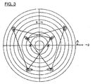
- Fig. 2 shows an X-ray diffraction pole figure obtained by this analysis. This X-ray diffraction pole figure was obtained when X-rays were incident on the (200) plane of the Al electrode layer 4. As shown in Fig. 3, additional lines were drawn for illustrating the diffraction pattern shown in Fig. 2.
- the Al electrode layer 4 was a thin epitaxial film in which diffraction spots having a plurality of symmetry spots were observed in the X-ray diffraction pole figure when X-rays were incident on the (200) plane of the Al.
- Six spots in Figs. 2 and 3 show the detection of reflection signals from the (200) plane of the Al.
- the six diffraction spots thus detected were two sets of three-fold symmetry spots.
- the angular distance between each spot and the corresponding symmetry center in the ⁇ direction was approximately 55°, and each symmetry center approximately coincided with the [111] direction of Al.
- the symmetry center and the normal line (the center of the pole figure) of the piezoelectric substrate 2 were apart from each other by ⁇ 10 to 20° in the ⁇ direction.
- the distance between the symmetry center and the center of the pole figure was approximately 17° in the ⁇ direction.
- this angle varies in accordance with conditions of the piezoelectric substrate 2, a film-forming temperature, or the like, in consideration of this variation, the distance can be considered to be in the range of ⁇ 10 to 20° as described above.
- the fact that the three-fold symmetry spots were observed means that the [111] direction of Al was oriented so as to approximately coincide with the center of the symmetry spots, that is, a triaxial orientation film was formed in which the Al[111] axis was grown in the direction toward the symmetry center.
- the fact that the two sets of three-fold symmetry spots were observed means that the two centers of the symmetry spots were present, and that the Al[111]-oriented crystal had two growing directions. In other words, the [111]-oriented single-crystal Al grew in two orientation directions, that is, the twin structure was formed.
- the film forming the Al electrode layer 4 is a triaxial-orientation epitaxial film formed of Al(111) oriented in two growing directions and is also a polycrystalline film having a twin structure.
- the electrode 3 was formed into an interdigital shape using a photolithographic technique and a dry etching technique, thereby forming the surface acoustic wave filter as the surface acoustic wave device 1.
- a service life (time until failure) of the filter formed in the first example was 1,000 times or more that of the filter formed in the comparative example.
- a piezoelectric substrate 2 composed of a 42° Y-cut LiTaO3 single crystal was prepared. Subsequently, in a process equivalent to that in the first example, the underlying electrode layer 5 was formed, and the Al electrode layer 4 was formed thereon.
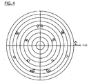
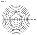
- Fig. 4 shows an X-ray diffraction pole figure obtained in this second example in which X-rays were incident on the (200) plane of the Al electrode layer 4. As shown in Figs. 5 and 6, additional lines were drawn for illustrating the diffraction pattern shown in Fig. 4.
- the Al electrode layer 4 was a thin epitaxial film in which diffraction spots having a plurality of symmetry centers were observed. Twelve spots in Figs. 4, 5 and 6 show the detection of reflection signals from the (200) plane of the Al.
- the twelve diffraction spots thus detected were two sets of six-fold symmetry spots.
- the angular distance between each spot and the corresponding symmetry center in the ⁇ direction was approximately 55°, and each symmetry center approximately coincided with the [111] direction of Al.
- the symmetry center and the normal line (the center of the pole figure) of the piezoelectric substrate 2 were apart from each other by ⁇ 10 to 20° in the ⁇ direction.
- the six-fold symmetry spots in themselves mean the formation of a twin.
- the reason for this is that when X-rays are incident on the Al(200) plane, the diffraction spots from the Al(111) single crystal are detected as three-fold symmetry spots each located at a position apart from the symmetry center by approximately 55°. More particularly, they are three symmetry spots, i.e., (100), (010), and (001). That is, the six-fold symmetry spots are formed of two sets of three-fold symmetry spots, as shown in Fig. 6, and these two sets of three-fold symmetry spots have a positional relationship with each other in which one set is located at a position rotated by 180° from that of the other set.
- this Al electrode layer 4 can also be regarded as "a twin formed of two twins" (four single domains are present). That is, when it is assumed that the two sets of three-fold symmetry spots shown in Fig. 2 each indicate a twin, the film structure described above may be easily understood.
- the Al electrode layer 4 obtained in the second example is also a triaxial epitaxial film formed of the Al(111) oriented in two growing directions and is essentially the same as that in the first example.
- the electrode 3 was formed into an interdigital shape using a photolithographic technique and a dry etching technique, thereby forming a surface acoustic wave filter as the surface acoustic wave device 1.
- a surface acoustic wave filter having an Al electrode layer which was a uniaxial orientation film, was also formed as a comparative example in which the Al(111) plane grew perpendicular to the piezoelectric substrate 2.
- the electrical power resistance of the surface acoustic wave filter formed in the second example was 1,000 times or more that of the comparative example. That is, concerning the electrical power resistance, it was understood that the advantage in the second example is equivalent to that in the first example.
- a surface acoustic wave filter was formed having the structure shown in Fig. 1 as the surface acoustic wave device 1.
- a piezoelectric substrate 2 composed of a 36° Y-cut LiTaO3 single crystal was prepared.
- the underlying electrode layer 5 was formed by an electron beam deposition method using Ti at a temperature of 70°C so as to have a thickness of 20 nm, and was then cooled to a temperature of 50°C or less in an evacuated state.
- the Al electrode layer 4 was formed using Al so as to have a thickness of 100 nm.
- the Al electrode layer 4 thus formed had a half value width of the Al(111) of approximately 2° measured by X-ray diffraction.
- the half value width of the Al(111) thereof was approximately 5°. According to the third example described above, it was confirmed that significantly higher orientation can be obtained.
- the electrode 3 was formed into an interdigital shape using a photolithographic technique and a dry etching technique, thereby forming the surface acoustic wave filter as the surface acoustic wave device 1.
- a surface acoustic wave filter was formed as a surface acoustic wave device 1a having the structure shown in Fig. 8.
- a piezoelectric substrate 2 composed of a 36° Y-cut LiTaO3 single crystal was prepared.
- the underlying electrode layer 5 was formed by an electron beam deposition method using Ti at a temperature of 70°C so as to have a thickness of 10 nm, and was then cooled to a temperature of 50°C or less in an evacuated state.
- the Al electrode layer 4 was then formed using Al so as to have a thickness of 100 nm.
- the Al electrode layer 4 thus formed had a half value width of the Al(111) of approximately 1.8° measured by X-ray diffraction. According to the fourth example, it was confirmed that a layer having significantly high orientation can be obtained as compared to those obtained in the comparative example and the third example.
- the electrode 3 was formed into an interdigital shape using a photolithographic technique and a dry etching technique, thereby forming the surface acoustic wave filter as the surface acoustic wave device 1a.
- this surface acoustic wave filter of the fourth example was compared with those of the comparative example and the third example by applying a constant electrical power, a service life of the filter in the fourth example was long as compared to the other filters described above.
- a surface acoustic wave filter was formed as the surface acoustic wave device 1a having the structure shown in Fig. 8.
- a piezoelectric substrate 2 composed of a 36° Y-cut LiTaO3 single crystal was prepared and was then processed by pretreatment using a buffered hydrogen fluoride (BHF) solution at room temperature for ten minutes, thereby removing a deteriorated layer which was present on the surface of the piezoelectric substrate 2 and inhibited epitaxial growth.
- BHF buffered hydrogen fluoride
- the underlying electrode layer 5 was formed by an electron beam deposition method using Ti at a temperature of 180°C so as to have a thickness of 10 nm and was then cooled to room temperature in an evacuated state.
- the intermediate electrode layer 6 composed of Ti, which was the same material as that for the underlying electrode layer 5, was formed so as to have a thickness of 10 nm.
- the Al electrode layer 4 was then formed using Al so as to have a thickness of 100 nm.
- the Al electrode layer 4 was a thin epitaxial film in which six diffraction spots were observed in the X-ray diffraction pole figure obtained when X-rays were incident on the Al(200) plane. Since reflection signals from the Al(200) plane were detected as two sets of three-fold symmetry spots, it was confirmed that the film forming the Al electrode layer 4 is a triaxial orientation film and is also a polycrystalline film having a twin structure.
- the electrode 3 was formed into an interdigital shape using a photolithographic technique and a dry etching technique, thereby forming the surface acoustic wave filter as the surface acoustic wave device 1a.
- a surface acoustic wave filter was formed as the surface acoustic wave device 1a having the structure shown in Fig. 8.
- a piezoelectric substrate 2 composed of a 42° Y-cut LiTaO3 single crystal was prepared. Subsequently, by using a process equivalent to that in the third example, the underlying electrode layer 5, the intermediate electrode layer 6, and the Al electrode layer 4 were formed on the piezoelectric substrate 2 in that order.
- the twelve diffraction spots thus detected shown in Fig. 4 were two sets of six-fold symmetry spots.
- the angular distance between each symmetry spot and the corresponding symmetry center in the ⁇ direction was approximately 55°, and each symmetric center approximately coincided with the [111] direction of Al.
- the symmetry center and the normal line (the center of the pole figure) of the piezoelectric substrate 2 were apart from each other by ⁇ 10 to 20° in the ⁇ direction.
- the distance between the symmetry center and the center of pole figure was approximately 17° in the ⁇ direction.
- this angle varies in accordance with conditions of the piezoelectric substrate 2, a film-forming temperature, or the like, in consideration of this variation, the distance can be considered to be in the range of ⁇ 10 to 20° as described above.
- the fact that six-fold symmetry spots were observed means that the [111] direction of Al was oriented so as to approximately coincide with the center of the symmetry center, that is, a triaxial orientation film was formed in which the Al[111]-oriented film was grown in the direction toward the symmetry center.
- the six-fold symmetry spots in themselves mean the formation of a twin.
- the reason for this is that when X-rays are incident on the Al(200) plane, the diffraction spots from the Al(111) single crystal are detected as three-fold symmetry spots each located at positions apart from the symmetry center by approximately 55°. More particularly, they are three symmetry spots, i.e., (100), (010), and (001).
- the fact that two sets of three-fold symmetry spots were observed means that the two centers of the symmetry spots were present, and that the Al[111]-oriented crystal had two growing directions. In other words, the [111]-oriented single-crystal Al grew in two orientation directions, that is, the twin structure was formed.
- these two sets of three-fold symmetry spots have a positional relationship with each other in which one set is located at a position rotated by 180° from that of the other set.
- this Al electrode layer 4 having this film structure can also be regarded as "a twin formed of two twins" (four single domains are present). That is, it may be assumed that the two sets of the three-fold symmetry spots shown in Fig. 3 each form a twin.
- the Al electrode layer 4 obtained in the sixth example is also a triaxial orientation epitaxial film formed of Al(111) oriented in two growing directions and is essentially the same as that in the second example.
- the electrode 3 was formed into an interdigital shape using a photolithographic technique and a dry etching technique, thereby forming the surface acoustic wave filter as the surface acoustic wave device 1.
- a surface acoustic wave filter having an Al electrode layer which was a uniaxial orientation film, was also formed as a comparative example in which the Al (111) plane grew perpendicular to the piezoelectric substrate 2.
- the electrical power resistance of the surface acoustic wave filter formed in the sixth example was 1,000 times or more that of the comparative example.
- the piezoelectric substrate 2 a 36° Y-cut LiTaO3 substrate and a 42° Y-cut LiTaO3 substrate were used; however, in addition to those described above, any substrate formed of a piezoelectric single crystal may be used.
- the cut angle of the Y-cut is preferably in the range of from 36° to 42°.
- the piezoelectric single crystal material for the piezoelectric substrates a single crystal formed of LiTaO3 or LiNbO3 is preferably used as the piezoelectric substrates.
- a film-forming temperature therefor was set to 180°C; however, the temperature is not limited thereto. It has been confirmed that when this film-forming temperature is changed, the spot intensity of the X-ray diffraction pole figure obtained when the X-rays are incident on the Al(200) plane varies as shown in Fig. 7.
- the film-forming temperature for the underlying electrode layer 5 when the film-forming temperature for the underlying electrode layer 5 is set to 70°C or more, diffraction spots of the Al electrode layer 4 formed thereon are detected, and an epitaxial Al film having a twin structure can be formed.
- the Ti film-forming temperature for forming the underlying electrode layer 5 is preferably set to a higher temperature.
- the film-forming temperature is preferably set to 300°C or less in practice.
- the electrode layer is primarily formed of Al; however, when a metal is used which has a face-centered cubic lattice and is primarily composed of platinum (Pt), gold (Au), copper (Cu), or silver (Ag), the same advantages as those described above can be obtained.
- the electrode layer which forms the electrode provided on the piezoelectric substrate composed of a piezoelectric single crystal, is an orientation film formed by epitaxial growth and is also a polycrystalline thin film having a twin structure in which a diffraction pattern observed in an X-ray diffraction pole figure has a plurality of symmetry centers, the formation of hillocks and/or voids in the electrode can be suppressed, and in addition, plastic deformation thereof becomes unlikely to occur, thereby improving the electrical power resistance of the surface acoustic wave device.
- the crystallinity of the electrode layer can be further improved.
- the method for manufacturing a surface acoustic wave device may further comprise a step of forming an intermediate electrode layer on the underlying electrode layer at a low temperature of 50°C or less in order to place a crystal face present on the surface of the underlying electrode layer in a cleaner state, and the Al electrode layer is formed on this intermediate electrode layer.
- a cleaner crystal face for forming the Al electrode layer can be obtained by the presence of the intermediate electrode layer while high orientation properties are maintained, thereby further improving the crystallinity of the Al electrode layer.
- the piezoelectric property can be improved, and when the surface acoustic wave device constitutes a filter or the like, the usable bandwidth therefor can be increased.
- a step for performing the etching treatment for the piezoelectric substrate may be provided to expose a crystal face on the surface thereof so that the Al electrode layer can be grown by epitaxial growth.
- the underlying electrode layer may be formed by heating to a temperature of 70°C or more, and subsequently, the Al electrode layer is formed at a low temperature of 50°C or less.
Landscapes
- Physics & Mathematics (AREA)
- Acoustics & Sound (AREA)
- Engineering & Computer Science (AREA)
- Manufacturing & Machinery (AREA)
- Surface Acoustic Wave Elements And Circuit Networks Thereof (AREA)
Abstract
Description
Patent publication 1: Japanese Unexamined Patent Application Publication No. 7-162255
Patent publication 2: Japanese Unexamined Patent Application Publication No. 3-48511
Patent publication 3: Japanese Unexamined Patent Application Publication No. 6-6173
Non-patent publication 1: "Technical Handbook of Surface acoustic wave device" edited by the 150th Committee on Technology of Surface acoustic wave device of the Japan Society for the Promotion of Science, published by Ohmsha, Ltd., p. 267.
Claims (24)
- A surface acoustic wave device comprising:wherein the electrode includes an oriented electrode layer (4) which is formed by epitaxial growth, said electrode layer (4) being a polycrystalline thin film having a twin structure in which a diffraction pattern observed in an X-ray diffraction pole figure has a plurality of symmetry centers.a piezoelectric substrate (2) made of a piezoelectric single crystal; andat least one electrode (3) provided on the piezoelectric substrate,
- A surface acoustic wave device according to Claim 1, wherein the electrode layer (4) comprises Al as a primary component.
- A surface acoustic wave device according to Claim 1 or 2, wherein the electrode (3) further comprises an underlying electrode layer (5) provided between the electrode layer (4) and the piezoelectric substrate (2) for improving the crystallinity of the electrode layer (4).
- A surface acoustic wave device according to Claim 3, wherein the underlying electrode layer (5) comprises at least one of Ti and Cr as a primary component.
- A surface acoustic wave device according to Claim 3 or 4, wherein the electrode (3) further comprises an intermediate electrode layer (6) between an Al electrode layer (4) and the underlying electrode layer (5) so as to cause a crystal face present on the surface of the underlying layer (5) to be in a cleaner state.
- A surface acoustic wave device according to any one of Claims 1 to 5, wherein the piezoelectric substrate (2) comprises a LiNbO3 or a LiTaO3 single crystal.
- A surface acoustic wave device according to Claim 6, wherein the piezoelectric substrate (2) is a rotation Y-cut LiTaO3 substrate in which is in the range of from 36° to 42°.
- A surface acoustic wave device according to any previous Claim, wherein, when X-rays are incident on the (200) plane of the crystal constituting the electrode layer (4), the [111] direction of the crystal is oriented so as to approximately coincide with the center of symmetry spots detected in the X-ray diffraction pole figure.
- A surface acoustic wave device according to any one of Claims 1 to 7, wherein, when X-rays are incident on the (200) plane of the crystal constituting the electrode layer (4), symmetry spots having at least two centers are observed in the X-ray diffraction pole figure, the crystal of the electrode layer grows in at least two [111] directions, and the [111] directions of the crystal are oriented so as to approximately coincide with the centers of the symmetry spots detected in the X-ray diffraction pole figure.
- A surface acoustic wave device according to Claim 9, wherein the symmetry spots detected in the X-ray diffraction pole figure form three-fold or six-fold symmetry.
- A method of manufacturing a surface acoustic wave (SAW) device comprising a piezoelectric substrate (2) made of a piezoelectric single crystal, and at least one electrode (3) provided on the piezoelectric substrate, the method comprising the steps of:providing a piezoelectric substrate (2), andepitaxially growing an oriented electrode layer (4), said electrode layer being a polycrystalline thin film having a twin structure in which a diffraction pattern observed in an X-ray diffraction pole figure has a plurality of symmetry centers.
- A SAW device manufacturing method according to claim 11, wherein:the step of providing a piezoelectric substrate comprises providing a substrate (2) formed of a Y-cut piezoelectric single crystal;the step of epitaxially growing an electrode layer comprises growing an Al electrode layer (4) primarily composed of Al; andthere is further provided the steps of:performing etching treatment for the piezoelectric substrate (2) to expose a crystal face on the surface of the piezoelectric substrate so that the Al electrode layer (4) is to be formed by epitaxial growth; andforming an underlying electrode layer (5) on a surface of the piezoelectric substrate (2), between the piezoelectric substrate (2) and the Al electrode layer (4), for improving the crystallinity of the Al electrode layer (4).
- A SAW device manufacturing method according to claim 12, wherein the step of performing etching treatment is performed using an etchant containing at least one selected from the group consisting of phosphoric acid, pyrophosphoric acid, benzoic acid, octanoic acid, hydrochloric acid, nitric acid, sulfuric acid, hydrofluoric acid, buffered hydrofluoric acid (BHF), and potassium hydrogen sulfate.
- A SAW device manufacturing method according to claim 11, 12 or 13, wherein the step of epitaxially growing an electrode layer comprises growing an Al electrode layer (4) at a temperature of 50°C or less, the Al electrode layer (4) being primarily composed of Al; and
there are provided the steps of:forming an underlying electrode layer (5) on a surface of the piezoelectric substrate (2) by heating to a temperature of 70°C or more, said underlying electrode (5) being formed between the piezoelectric substrate (2) and the Al electrode later (4) for improving the crystallinity of the Al electrode layer (4). - A SAW device manufacturing method according to Claim 14, wherein the step of forming the underlying electrode layer (5) is performed at a temperature of 300°C or less.
- A SAW device manufacturing method according to Claim 14 or 15, wherein the step of forming the Al electrode layer (4) is performed at a temperature of 0°C or more.
- A SAW device manufacturing method according to Claim 11, 14, 15 or 16, wherein the piezoelectric substrate (2) comprises a Y-cut piezoelectric single crystal.
- A SAW device manufacturing method according to any one of Claims 11 to 17, wherein the piezoelectric substrate (2) comprises a LiNbO3 or a LiTaO3 single crystal.
- A SAW device manufacturing method according to Claim 18, wherein the piezoelectric substrate (2) is a rotation Y-cut LiTaO3 substrate in which is in the range of from 36° to 42°.
- A SAW device manufacturing method according to any one of Claims 11 to 19, comprising the step of forming an underlying electrode layer (5) between the piezoelectric substrate (2) and the electrode layer (4), said underlying electrode layer (5) comprising at least one of Ti and Cr as a primary component.
- A SAW device manufacturing method according to any one of Claims 11 to 20, comprising the steps of:wherein an Al electrode layer (4) is formed on the intermediate electrode layer (6) in the step of growing the electrode layer.forming an underlying electrode layer (5) between the piezoelectric substrate (2) and the electrode layer (4), andforming an intermediate electrode layer (6) on the underlying electrode layer (5) at a temperature of 50°C or less for placing a crystal face present on the underlying electrode layer in a cleaner state,
- A SAW device manufacturing method according to Claim 21, wherein the intermediate electrode layer (6) comprises at least one of Ti and Cr as a primary component.
- A SAW device manufacturing method according to Claim 21 or 22, wherein the intermediate electrode layer (6) comprises the same material as that for the underlying electrode layer (5).
- A SAW device manufacturing method according to any one of Claims 21 to 23, wherein the step of forming the intermediate electrode layer (6) is performed at a temperature of 0°C or more.
Applications Claiming Priority (8)
| Application Number | Priority Date | Filing Date | Title |
|---|---|---|---|
| JP2001397851 | 2001-12-27 | ||
| JP2001397850 | 2001-12-27 | ||
| JP2001397851 | 2001-12-27 | ||
| JP2001397850 | 2001-12-27 | ||
| JP2002341691 | 2002-11-26 | ||
| JP2002341691A JP3938021B2 (en) | 2001-12-27 | 2002-11-26 | Manufacturing method of surface acoustic wave device |
| JP2002341690A JP2003258594A (en) | 2001-12-27 | 2002-11-26 | Surface acoustic wave device and manufacturing method therefor |
| JP2002341690 | 2002-11-26 |
Publications (3)
| Publication Number | Publication Date |
|---|---|
| EP1324487A2 true EP1324487A2 (en) | 2003-07-02 |
| EP1324487A3 EP1324487A3 (en) | 2004-08-04 |
| EP1324487B1 EP1324487B1 (en) | 2008-08-20 |
Family
ID=27482754
Family Applications (1)
| Application Number | Title | Priority Date | Filing Date |
|---|---|---|---|
| EP02293252A Expired - Lifetime EP1324487B1 (en) | 2001-12-27 | 2002-12-27 | Surface acoustic wave device and manufacturing method therefor |
Country Status (6)
| Country | Link |
|---|---|
| US (2) | US6822371B2 (en) |
| EP (1) | EP1324487B1 (en) |
| KR (1) | KR100477847B1 (en) |
| CN (1) | CN1246959C (en) |
| DE (1) | DE60228396D1 (en) |
| TW (1) | TWI282660B (en) |
Cited By (3)
| Publication number | Priority date | Publication date | Assignee | Title |
|---|---|---|---|---|
| EP1722473A4 (en) * | 2004-03-05 | 2008-07-30 | Murata Manufacturing Co | SOUND ACOUSTIC WAVE DEVICE |
| EP1786099A3 (en) * | 2005-11-10 | 2010-07-07 | Nihon Dempa Kogyo Co., Ltd. | Surface acoustic wave device and method of manufacturing the same |
| US9173305B2 (en) | 2009-12-02 | 2015-10-27 | Epcos Ag | Metallization having high power compatibility and high electrical conductivity |
Families Citing this family (8)
| Publication number | Priority date | Publication date | Assignee | Title |
|---|---|---|---|---|
| JP4096787B2 (en) * | 2003-04-11 | 2008-06-04 | 株式会社村田製作所 | Manufacturing method of surface acoustic wave device |
| JP2005347892A (en) * | 2004-05-31 | 2005-12-15 | Fujitsu Media Device Kk | Surface acoustic wave device |
| WO2006016544A1 (en) * | 2004-08-11 | 2006-02-16 | Murata Manufacturing Co., Ltd. | Duplexer and communication apparatus |
| JPWO2009150786A1 (en) * | 2008-06-09 | 2011-11-10 | 株式会社村田製作所 | Surface acoustic wave device and manufacturing method thereof |
| JP2011109306A (en) * | 2009-11-16 | 2011-06-02 | Murata Mfg Co Ltd | Surface acoustic wave element |
| CN106603035A (en) * | 2016-12-23 | 2017-04-26 | 北京中科飞鸿科技有限公司 | Method for improving tolerance power of surface acoustic wave filter |
| CN109660224B (en) * | 2018-12-18 | 2023-03-24 | 北方民族大学 | Composite piezoelectric substrate for filter and preparation method thereof |
| KR102806885B1 (en) | 2023-03-28 | 2025-05-14 | (주)와이솔 | Surface acoustic wave including advanced electrode structure and manufacturing method of the same |
Family Cites Families (23)
| Publication number | Priority date | Publication date | Assignee | Title |
|---|---|---|---|---|
| JPS56149811A (en) * | 1980-04-23 | 1981-11-19 | Hitachi Ltd | Elastic surface wave device and its preparation |
| US4634913B1 (en) * | 1980-06-11 | 1997-05-13 | Plessey Co Ltd | Application of lithium tetraborate to electronic devices |
| JP2665597B2 (en) | 1988-05-02 | 1997-10-22 | マツダ株式会社 | Torque converter slip controller |
| US5162690A (en) * | 1989-04-14 | 1992-11-10 | Murata Manufacturing Co., Ltd. | Surface acoustic wave device |
| JP2545983B2 (en) | 1989-04-14 | 1996-10-23 | 株式会社村田製作所 | Surface acoustic wave device |
| JPH0340510A (en) | 1989-07-06 | 1991-02-21 | Murata Mfg Co Ltd | Elastic surface wave device |
| JP3040510B2 (en) | 1991-03-06 | 2000-05-15 | 日本碍子株式会社 | Honeycomb heater |
| JPH066173A (en) | 1992-06-19 | 1994-01-14 | Hitachi Ltd | Surface acoustic wave device electrode |
| US5446330A (en) * | 1993-03-15 | 1995-08-29 | Matsushita Electric Industrial Co., Ltd. | Surface acoustic wave device having a lamination structure |
| JP3379049B2 (en) * | 1993-10-27 | 2003-02-17 | 富士通株式会社 | Surface acoustic wave device and method of manufacturing the same |
| US5650362A (en) * | 1993-11-04 | 1997-07-22 | Fuji Xerox Co. | Oriented conductive film and process for preparing the same |
| JP3208977B2 (en) | 1993-12-02 | 2001-09-17 | 株式会社村田製作所 | Method for forming electrodes of surface acoustic wave device |
| JP2888158B2 (en) | 1995-01-18 | 1999-05-10 | 日本電気株式会社 | Manufacturing method of surface acoustic wave device |
| JP3106912B2 (en) | 1995-06-30 | 2000-11-06 | 株式会社村田製作所 | Method of manufacturing edge reflection type surface acoustic wave device |
| JP3230465B2 (en) | 1997-09-05 | 2001-11-19 | 日産自動車株式会社 | Slip control device for torque converter |
| EP0940914B1 (en) | 1997-09-22 | 2003-10-15 | TDK Corporation | Surface acoustic wave apparatus and method of production thereof |
| JP3183235B2 (en) | 1997-11-04 | 2001-07-09 | 日産自動車株式会社 | Slip control device for torque converter |
| JP3240979B2 (en) | 1997-11-04 | 2001-12-25 | 日産自動車株式会社 | Slip control device for torque converter |
| KR100455493B1 (en) | 1998-10-16 | 2004-11-08 | 세이코 엡슨 가부시키가이샤 | Surface acoustic wave device |
| JP3635946B2 (en) | 1998-11-06 | 2005-04-06 | 日産自動車株式会社 | Slip control device for torque converter |
| JP3601346B2 (en) | 1999-02-25 | 2004-12-15 | 日産自動車株式会社 | Slip control device for torque converter |
| WO2000074235A1 (en) | 1999-05-31 | 2000-12-07 | Tdk Corporation | Surface acoustic wave device |
| JP3846221B2 (en) * | 2000-07-14 | 2006-11-15 | 株式会社村田製作所 | Surface acoustic wave device |
-
2002
- 2002-12-24 TW TW091137116A patent/TWI282660B/en not_active IP Right Cessation
- 2002-12-26 KR KR10-2002-0084035A patent/KR100477847B1/en not_active Expired - Lifetime
- 2002-12-27 US US10/329,338 patent/US6822371B2/en not_active Expired - Lifetime
- 2002-12-27 CN CNB021605033A patent/CN1246959C/en not_active Expired - Lifetime
- 2002-12-27 EP EP02293252A patent/EP1324487B1/en not_active Expired - Lifetime
- 2002-12-27 DE DE60228396T patent/DE60228396D1/en not_active Expired - Lifetime
-
2004
- 2004-09-30 US US10/953,348 patent/US7146695B2/en not_active Expired - Lifetime
Cited By (4)
| Publication number | Priority date | Publication date | Assignee | Title |
|---|---|---|---|---|
| EP1722473A4 (en) * | 2004-03-05 | 2008-07-30 | Murata Manufacturing Co | SOUND ACOUSTIC WAVE DEVICE |
| EP1786099A3 (en) * | 2005-11-10 | 2010-07-07 | Nihon Dempa Kogyo Co., Ltd. | Surface acoustic wave device and method of manufacturing the same |
| US9173305B2 (en) | 2009-12-02 | 2015-10-27 | Epcos Ag | Metallization having high power compatibility and high electrical conductivity |
| US9728705B2 (en) | 2009-12-02 | 2017-08-08 | Qualcomm Incorporated | Metallization having high power compatibility and high electrical conductivity |
Also Published As
| Publication number | Publication date |
|---|---|
| KR20030057386A (en) | 2003-07-04 |
| US7146695B2 (en) | 2006-12-12 |
| KR100477847B1 (en) | 2005-03-22 |
| US20030132684A1 (en) | 2003-07-17 |
| DE60228396D1 (en) | 2008-10-02 |
| TW200301616A (en) | 2003-07-01 |
| TWI282660B (en) | 2007-06-11 |
| US6822371B2 (en) | 2004-11-23 |
| EP1324487A3 (en) | 2004-08-04 |
| EP1324487B1 (en) | 2008-08-20 |
| US20050057121A1 (en) | 2005-03-17 |
| CN1246959C (en) | 2006-03-22 |
| CN1430330A (en) | 2003-07-16 |
Similar Documents
| Publication | Publication Date | Title |
|---|---|---|
| CN1205744C (en) | Surface acoustic wave appts. and method of prodn. thereof | |
| US10553778B2 (en) | Piezoelectric device and method for manufacturing piezoelectric device | |
| JP4809042B2 (en) | Surface acoustic wave device and manufacturing method thereof | |
| US6630767B2 (en) | Surface acoustic wave device with improved electrode | |
| US7146695B2 (en) | Method for manufacturing a surface acoustic wave device with a piezoelectric substrate | |
| CN1303538A (en) | Surface acoustic wave device | |
| JPH07162255A (en) | Method for forming electrode for surface acoustic wave element | |
| JP4019693B2 (en) | Surface acoustic wave device | |
| TWI769270B (en) | Surface acoustic wave device and method for manufacturing the same | |
| JP2003258594A (en) | Surface acoustic wave device and manufacturing method therefor | |
| JP3308749B2 (en) | Method for manufacturing surface acoustic wave device, and surface acoustic wave device manufactured using the same | |
| JP3938021B2 (en) | Manufacturing method of surface acoustic wave device | |
| JP3317860B2 (en) | Surface acoustic wave device and method of manufacturing the same | |
| JP2004056355A (en) | Manufacturing method of thin film element | |
| JP4179307B2 (en) | Surface acoustic wave device and manufacturing method thereof | |
| JP2003069357A (en) | Method of manufacturing surface acoustic wave device and surface acoustic wave device | |
| JP2002353768A (en) | Surface acoustic wave element | |
| Sakurai et al. | Epitaxially grown aluminum film for high-power surface acoustic wave devices | |
| JP2004140732A (en) | Thin film element and method of manufacturing same | |
| HK1038837B (en) | Surface acoustic wave device | |
| JPWO1999016168A1 (en) | Surface acoustic wave device and manufacturing method thereof |
Legal Events
| Date | Code | Title | Description |
|---|---|---|---|
| PUAI | Public reference made under article 153(3) epc to a published international application that has entered the european phase |
Free format text: ORIGINAL CODE: 0009012 |
|
| 17P | Request for examination filed |
Effective date: 20030104 |
|
| AK | Designated contracting states |
Designated state(s): AT BE BG CH CY CZ DE DK EE ES FI FR GB GR IE IT LI LU MC NL PT SE SI SK TR |
|
| AX | Request for extension of the european patent |
Extension state: AL LT LV MK RO |
|
| PUAL | Search report despatched |
Free format text: ORIGINAL CODE: 0009013 |
|
| AK | Designated contracting states |
Kind code of ref document: A3 Designated state(s): AT BE BG CH CY CZ DE DK EE ES FI FR GB GR IE IT LI LU MC NL PT SE SI SK TR |
|
| AX | Request for extension of the european patent |
Extension state: AL LT LV MK RO |
|
| RIC1 | Information provided on ipc code assigned before grant |
Ipc: 7H 03H 3/08 B Ipc: 7H 03H 9/02 A |
|
| AKX | Designation fees paid |
Designated state(s): DE FR GB |
|
| RBV | Designated contracting states (corrected) |
Designated state(s): DE FR GB |
|
| 17Q | First examination report despatched |
Effective date: 20061222 |
|
| RAP1 | Party data changed (applicant data changed or rights of an application transferred) |
Owner name: MURATA MANUFACTURING CO., LTD. |
|
| GRAP | Despatch of communication of intention to grant a patent |
Free format text: ORIGINAL CODE: EPIDOSNIGR1 |
|
| GRAS | Grant fee paid |
Free format text: ORIGINAL CODE: EPIDOSNIGR3 |
|
| GRAA | (expected) grant |
Free format text: ORIGINAL CODE: 0009210 |
|
| AK | Designated contracting states |
Kind code of ref document: B1 Designated state(s): DE FR GB |
|
| REG | Reference to a national code |
Ref country code: GB Ref legal event code: FG4D |
|
| REF | Corresponds to: |
Ref document number: 60228396 Country of ref document: DE Date of ref document: 20081002 Kind code of ref document: P |
|
| PLBE | No opposition filed within time limit |
Free format text: ORIGINAL CODE: 0009261 |
|
| STAA | Information on the status of an ep patent application or granted ep patent |
Free format text: STATUS: NO OPPOSITION FILED WITHIN TIME LIMIT |
|
| 26N | No opposition filed |
Effective date: 20090525 |
|
| REG | Reference to a national code |
Ref country code: FR Ref legal event code: PLFP Year of fee payment: 14 |
|
| REG | Reference to a national code |
Ref country code: FR Ref legal event code: PLFP Year of fee payment: 15 |
|
| REG | Reference to a national code |
Ref country code: FR Ref legal event code: PLFP Year of fee payment: 16 |
|
| PGFP | Annual fee paid to national office [announced via postgrant information from national office to epo] |
Ref country code: FR Payment date: 20211224 Year of fee payment: 20 Ref country code: GB Payment date: 20211221 Year of fee payment: 20 Ref country code: DE Payment date: 20211210 Year of fee payment: 20 |
|
| REG | Reference to a national code |
Ref country code: DE Ref legal event code: R071 Ref document number: 60228396 Country of ref document: DE |
|
| REG | Reference to a national code |
Ref country code: GB Ref legal event code: PE20 Expiry date: 20221226 |
|
| PG25 | Lapsed in a contracting state [announced via postgrant information from national office to epo] |
Ref country code: GB Free format text: LAPSE BECAUSE OF EXPIRATION OF PROTECTION Effective date: 20221226 |