EP1324422A2 - Line coupling structure, mixer, and receiving/transmitting apparatus - Google Patents
Line coupling structure, mixer, and receiving/transmitting apparatus Download PDFInfo
- Publication number
- EP1324422A2 EP1324422A2 EP02028053A EP02028053A EP1324422A2 EP 1324422 A2 EP1324422 A2 EP 1324422A2 EP 02028053 A EP02028053 A EP 02028053A EP 02028053 A EP02028053 A EP 02028053A EP 1324422 A2 EP1324422 A2 EP 1324422A2
- Authority
- EP
- European Patent Office
- Prior art keywords
- coupling structure
- dielectric
- line coupling
- conductor pattern
- structure according
- Prior art date
- Legal status (The legal status is an assumption and is not a legal conclusion. Google has not performed a legal analysis and makes no representation as to the accuracy of the status listed.)
- Granted
Links
Images



Classifications
-
- H—ELECTRICITY
- H01—ELECTRIC ELEMENTS
- H01P—WAVEGUIDES; RESONATORS, LINES, OR OTHER DEVICES OF THE WAVEGUIDE TYPE
- H01P5/00—Coupling devices of the waveguide type
- H01P5/02—Coupling devices of the waveguide type with invariable factor of coupling
-
- H—ELECTRICITY
- H01—ELECTRIC ELEMENTS
- H01P—WAVEGUIDES; RESONATORS, LINES, OR OTHER DEVICES OF THE WAVEGUIDE TYPE
- H01P5/00—Coupling devices of the waveguide type
- H01P5/08—Coupling devices of the waveguide type for linking dissimilar lines or devices
- H01P5/10—Coupling devices of the waveguide type for linking dissimilar lines or devices for coupling balanced lines or devices with unbalanced lines or devices
- H01P5/1022—Transitions to dielectric waveguide
-
- H—ELECTRICITY
- H01—ELECTRIC ELEMENTS
- H01P—WAVEGUIDES; RESONATORS, LINES, OR OTHER DEVICES OF THE WAVEGUIDE TYPE
- H01P5/00—Coupling devices of the waveguide type
- H01P5/12—Coupling devices having more than two ports
- H01P5/16—Conjugate devices, i.e. devices having at least one port decoupled from one other port
- H01P5/18—Conjugate devices, i.e. devices having at least one port decoupled from one other port consisting of two coupled guides, e.g. directional couplers
Definitions
- the present invention relates to a line coupling structure for coupling a dielectric waveguide, in which signals such as millimeter waves propagate, to a suspended line.
- the present invention also relates to a mixer including such a line coupling structure and further relates to a receiving/transmitting apparatus including such a mixer.
- a diode mounting structure in a nonradiative dielectric waveguide (hereinafter referred to as an NRD guide) and a mixer with such a structure are disclosed in Kuroki and Yoneyama "Circuit Elements In Nonradiative Dielectric Waveguide Using Beam Lead Diodes", Journal of IEICE (The Institute of Electronics, Information and Communication Engineers), C-I, Vol J-73-C-I, No. 2, pp. 71-76 (February 1989).
- This mixer has a structure in which a coupler includes an NRD guide, and a circuit board carrying a diode is vertically sandwiched between dielectric strips to couple the diode to the NRD guide.
- the structure disclosed in the above-described document has various problems. Specifically, since the circuit board carrying the diode is arranged in a direction that is perpendicular to the lengthwise direction of the dielectric strips, the circuit board is difficult to be fixed and tends to tilt, which makes it difficult to mount. Insertion of a sheet having a high dielectric constant into the NRD guide, provision of a gap therein, or other measures are required to achieve matching in the structure, and therefore, the above-described structure cannot be easily designed and fabricated. In a coupler including the NRD guide, the greater the difference from the frequency at which the power distribution ratio is even, the higher the possibility that the power distribution ratio lacks balance.
- a mixer having a line coupling structure for coupling a dielectric waveguide to a suspended line is disclosed.
- a typical mixer disclosed in the above-described publication is shown in Fig. 6.
- Fig. 6 is a plan view showing the dielectric waveguide apparatus when an upper conductor plate is removed.
- a circuit board 4 and dielectric strips are sandwiched between two conductor plates including two parallel conductor planes (not shown in Fig. 6).
- a dielectric strip 3b in Fig. 6 is an upper dielectric strip disposed on the circuit board 4. Another dielectric strip facing the dielectric strip 3b is disposed beneath the circuit board 4.
- a beam lead diode 8 is mounted on and connected in series with the conductor pattern 5.
- the dielectric strip 3b is arranged such that it crosses the conductor pattern 5 in a direction that is perpendicular to the conductor pattern 5 at a predetermined distance from the inner end thereof.
- the line coupling structure for coupling the suspended line including the conductor pattern 5 and the upper and lower conductor plates to a NRD guide including the dielectric strip 3b and the upper and lower conductor plates is formed in such a manner.
- the dielectric waveguide apparatus described above has a structure in which LSM mode signals propagating in the dielectric waveguide have the same magnetic field direction as TEM mode signals propagating in the suspended line, the waveguide is easily and strongly coupled to the suspended line. Accordingly, this apparatus has various advantages including conversion loss in the mixer can be less than that in known apparatuses, and the simplified structure of the overall apparatus allows for easy manufacturing.
- the inventors of the present invention have discovered by experiment and determined that the transmission loss in a line coupling section between the dielectric waveguide and the suspended line can be further reduced.
- preferred embodiments of the present invention provide a line coupling structure that has lower transmission loss between a dielectric waveguide and a suspended line, a mixer including such a line coupling structure, and a receiving/transmitting apparatus including such a mixer.
- a line coupling structure has a dielectric waveguide that includes two conductor plates that are substantially parallel to each other and a dielectric strip, the dielectric strip and a circuit board being sandwiched between the two conductor plates, and a suspended line that includes the conductor plates and a conductor pattern on the circuit board.
- the conductor pattern and the dielectric strip are arranged so as to cross each other, thereby the dielectric waveguide and the suspended line are coupled each other.
- a protruding conductor pattern that extends in the extending direction of the dielectric strip is provided at a crossing position of the conductor pattern and the dielectric strip.
- Such a structure allows the degree of coupling between the dielectric waveguide and the suspended line to increase, thereby achieving lower line conversion loss and reduced transmission loss between the dielectric waveguide and the suspended line.
- the tip of the protruding conductor pattern is preferably located close to the position where a signal propagating in the dielectric waveguide has the maximum electric field component.
- the maximum electric field component is obtained at a position that is slightly inside the dielectric strip from the inner end thereof.
- a mixer including the line coupling structure according to the preferred embodiment described above.
- the dielectric strip and the conductor pattern are arranged, a diode is mounted on the conductor pattern, and an IF (intermediate frequency) signal is extracted from the conductor pattern, such that at least one of an RF (radio frequency) signal, a Lo signal, and a mixed signal of the RF signal and the Lo signal propagates in the suspended line.
- the mixer with such a structure can provide higher conversion efficiency.
- a receiving/transmitting apparatus includes a converter that converts a received signal into an IF signal.
- the mixer according to the preferred embodiment described above includes the converter.
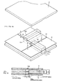
- Fig. 1A is an exploded perspective view showing the structure of a balanced mixer according to a preferred embodiment of the present invention when an upper conductor plate 2 is raised.
- Fig. 1B is a sectional view showing the structure of the balanced mixer according to this preferred embodiment.
- a lower conductor plate 1 and the upper conductor plate 2 constitute two conductor planes arranged substantially parallel to each other one above the other.
- First dielectric strips 31a and 31b and second dielectric strips 32a and 32b are vertically sandwiched between the two conductor plates 1 and 2.
- a circuit board 4 is sandwiched between the first dielectric strips 31a and 31b and between the second dielectric strips 32a and 32b.
- the conductor plates 1 and 2 have corresponding grooves into which the first dielectric strips 31a and 31b and the second dielectric strips 32a and 32b fit.
- the circuit board 4 while being supported by a peripheral support (not shown), lies vertically halfway between, and substantially parallel to, the lower conductor plate 1 and the upper conductor plate 2.
- the conductor plates 1 and 2 are joined at their peripheries (not shown) and, in a dielectric waveguide, they constitute the two conductor planes arranged substantially parallel one above the other, as shown in Figs. 1A and 1B.
- the dielectric strips 31a, 31b, 32a, and 32b are preferably made of dielectric materials such as resin or ceramic and have a substantially rectangular cross-section that is substantially perpendicular to the lengthwise direction thereof.
- the dielectric strips 31a, 31b, 32a, and 32b constitute a propagation area where electromagnetic signals propagates therealong, in which area a cut-off state is cleared.
- the portions other than the dielectric strips 31a, 31b, 32a, and 32b constitute a cut-off area where the signals in the propagation area are cut off and where the distance between the conductor plates 1 and 2 is less than ⁇ 0/2, where ⁇ 0 is the free space wavelength of propagating high-frequency signals.
- the distance h1 between the conductor plates 1 and 2 in the cut-off area, the distance h2 therebetween in the propagation area, and the thickness t of the circuit board 4, which are shown in Fig. 1B, and the respective dielectric constants of the dielectric strips 31a and 31b and the circuit board 4 are determined such that the cut-off frequency in an LSM01 mode is lower than that in an LSE01 mode in the propagation area and such that electromagnetic waves in the LSM01 and LSE01 modes are cut off in the cut-off area.
- the first dielectric strips 31a and 31b and the upper and lower conductor plates 1 and 2 constitute a first NRD guide in which single-mode transmission in the LSM01 mode can be performed.
- the second dielectric strips 32a and 32b and the upper and lower conductor plates 1 and 2 constitute a second NRD guide in which single-mode transmission in the LSM01 mode can be performed.
- a first conductor pattern 51 is arranged substantially perpendicular to the lengthwise direction of the dielectric strips 31a and 31b.
- the first conductor pattern 51 and the upper and lower conductor plates 1 and 2 constitute a first suspended line.
- the first conductor pattern 51 has a first filter circuit 6 and a second filter circuit 7 at the both sides of the first dielectric strips 31a and 31b disposed therebetween.
- the suspended line between the first filter circuit 6 and the second filter circuit 7 defines a first resonant circuit.
- two beam lead diodes 81 and 82 which are Schottky barrier diodes, are mounted on and in series with the conductor pattern 51.
- a second conductor pattern 52 extends from the boundary of the first and second filter circuits 6 and 7 in the lengthwise direction of the first dielectric strips 31a and 31b.
- the second conductor pattern 52 and the upper and lower conductor plates 1 and 2 constitute a second suspended line.
- a third filter circuit 9 is provided in the middle of the second conductor pattern 52 so that some signals propagating in the second conductor pattern 52 do not go beyond the third filter circuit 9.
- the second NRD guide which includes the second dielectric strips 32a and 32b and the upper and lower conductor plates 1 and 2, is magnetically coupled to the second conductor pattern 52.
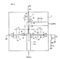
- Fig. 2 is a plan view of the balanced mixer when the upper conductor plate 2 is removed.
- Open stubs 6a, 6b, 7a, 7b, 9a, and 9b have a length of about ⁇ /4.
- the pair of open stubs 6a and 6b, 7a and 7b, and 9a and 9b are each arranged with a spacing of about ⁇ /4 therebetween.
- Each pair of the ⁇ /4-long open stubs at a spacing of about ⁇ /4 defines a band elimination filter (BEF) for blocking signals with a wavelength of ⁇ .
- BEF band elimination filter
- the respective electrical lengths of the distance L11 from the center of the first filter circuit 6 to the second filter circuit 7 and of the distance L12 from the center of the second filter circuit 7 to the first filter circuit 6 correspond to an integral multiple of about 1/2 of the wavelength at the frequency f1 of millimeter waves propagating in the first NRD guide. Accordingly, the suspended line between the filter circuits 6 and 7 functions as a resonant circuit with two short-circuited ends.
- the electrical length of the distance L2 from the center portion between the first filter circuit 6 and the second filter circuit 7 to the open stub 9a is an integral multiple of about 1/2 of the wavelength at the frequency f2 of millimeter waves propagating in the second NRD guide including the second dielectric strips 32a and 32b.
- the center portion between the first filter circuit 6 and the second filter circuit 7 is equivalently short-circuited. Accordingly, the suspended line having the distance L2 also functions as a resonant circuit with two short-circuited ends.
- the two beam lead diodes 81 and 82 are mounted on and in series with the conductor pattern 51.
- the LSM01 mode signals propagating in the first NRD guide including the first dielectric strips 31a and 31b and the upper and lower conductor plates 1 and 2 easily couples with the TEM mode signals in the suspended line including the first resonant circuit.
- the relative arrangement between the first NRD guide and the suspended line, the positions of diodes 81 and 82, the positions of the filter circuits 6 and 7 and so on are determined such that the reflection loss from the inner end of the first NRD guide or the conversion loss in the mixer is minimized at a desired frequency (for example, f1).
- the second conductor pattern 52 is magnetically coupled to the second NRD guide including the second dielectric strips 32a and 32b and the upper and lower conductor plates 1 and 2.
- a first RF signal for example, a received signal RX
- a second RF signal for example, a local signal Lo
- a bias voltage supply circuit including an inductance coil Lb, a resistance Rb, and power source Vb is connected to the first conductor pattern 51.
- One end of the conductor pattern 51 is AC-grounded through a capacitor Cg.
- the inductance coil Lb prevents the leakage of an IF signal into the bias voltage supply circuit.
- the resistance Rb sets a bias current for the diodes to reduce conversion loss.
- the first and second RF signals from the second NRD guide are applied to the two diodes 81 and 82 at a phase difference of about 180°, so that the frequency components of the differences between the first and second RF signals entering from the second NRD guide and the second and first RF signals entering from the first NRD guide have reverse phases with respect to each other. Since the two diodes 81 and 82 are arranged to have opposite orientations with respect to each other when they are viewed from the IF end, the frequency components of the differences mentioned above can be combined in phase to be extracted as the IF signal through a capacitor Ci.
- a protruding conductor pattern 11 extends from the crossing position of the first conductor pattern 51 and the first dielectric strips 31a and 31b and has a length x in the extending direction of the first dielectric strips 31a and 31b.
- a protruding conductor pattern 10 extends from the crossing position of the second conductor pattern 52 and the second dielectric strips 32a and 32b and has a length x in the extending direction of the second dielectric strips 32a and 32b.
- the provision of the protruding conductor patterns 10 or 11 at the position having a higher electric field component in a main propagation mode in the NRD guide causes the degree of coupling between the suspended line and the dielectric waveguide to increase.
- Fig. 3 shows an example of dimensions for obtaining the characteristics of a line conversion section with respect to the second NRD guide having the second conductor pattern 52 and the second dielectric strips 32a and 32b shown in Fig. 2.
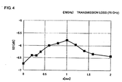
- Fig. 4 is a graph showing the transmission loss in the line conversion section.
- the width of the cut-off area is determined in the second NRD guide including the second dielectric strips 32a and 32b and the upper and lower conductor plates 1 and 2, using the second dielectric strips 32a and 32b having a relative dielectric constant ( ⁇ r) of about 2.04, with the inner ends of the dielectric strips being open. Similarly, the width of the suspended line is determined.
- the transmission loss (S parameter S21) between the outer end of the NRD guide (port 1) in the LSM01 mode and the outer end of the suspended line (port 2) in the TEM mode is calculated at a frequency of about 76 GHz by a FEM (finite element method) when the length x of the protruding conductor pattern in Fig. 3 is varied.
- the electric field strength reaches a maximum at a position slightly inside the NRD guide from the inner end.
- the suspended line has a maximum voltage at the open end. Accordingly, the highest degree of coupling is achieved when an open end of the suspended line is at the position where the NRD guide has the maximum electric field strength.
- the provision of the protruding conductor pattern allows the line conversion loss between the NRD guide and the suspended line to be decreased.
- the conversion loss therein can be reduced over a larger bandwidth.
- a single mixer can be provided. Specifically, referring to Figs. 1A and 1B and 2, a mixed signal of the first RF signal and the second RF signal is inputted from the first NRD guide including the first dielectric strips 31a and 31b, without the second conductor pattern 52, the second dielectric strips 32a and 32b, and the diode 82 (without pattern gaps in the diode 82), and the IF signal is outputted from the conductor pattern 51.
- Fig. 5 shows a typical structure of a millimeter-wave radar module of a receiving/transmitting apparatus according to another preferred embodiment of the present invention.
- a block diagram of the millimeter-wave radar module is shown in Fig. 5.
- a voltage controlled oscillator VCO uses, for example, a Gunn diode and a varactor diode.
- An isolator ISO prevents a reflected signal from returning to the VCO.
- a coupler CPL is a directional coupler including a NRD guide for extracting a portion of a transmitter signal as the local signal Lo.
- a circulator CIR provides the transmitter signal to a scan unit and transmits a receiver signal RX to a mixer MIX.
- the mixer MIX mixes the receiver signal RX and the local signal Lo to output an IF signal.
- the mixer shown in Figs. 1A and 1B and 2 defines the mixer MIX.
- a millimeter-wave radar apparatus has the above-described millimeter-wave radar module and a control section for providing a modulation signal to calculate the relative distance and the relative speed of a target using the IF signal.
Landscapes
- Waveguides (AREA)
- Waveguide Connection Structure (AREA)
- Transceivers (AREA)
- Control Of Motors That Do Not Use Commutators (AREA)
Abstract
Description
Claims (18)
- A line coupling structure comprising:wherein a protruding conductor pattern (52) that extends in the extending direction of the dielectric strip (31a,31b) is provided at a crossing portion of the conductor pattern (51) and the dielectric strip (31a,31b).a dielectric waveguide including a dielectric strip (31a,31b) and two conductor plates (1,2) that are substantially in parallel with each other, the dielectric strip (31a,31b) and a circuit board (4) being sandwiched between the two conductor plates (31a, 31b); anda suspended line including the conductor plates (1,2) and a conductor pattern (51) on the circuit board, the conductor pattern (51) and the dielectric strip (31a,31b) being arranged so as to cross each other in order to be coupled with each other;
- The line coupling structure according to Claim 1, wherein the tip of the protruding conductor pattern (51) is located close to a position where a signal propagating in the dielectric waveguide has a maximum electric field component.
- The line coupling structure according to Claim 1, further comprising a plurality of dielectric strips (31a,31b,32a,32b), wherein the two conductor plates (1,2) have corresponding grooves into which the plurality of dielectric strips (31a,31b,32a,32b) are mounted.
- The line coupling structure according to Claim 3, wherein the plurality of dielectric strips (31a,31b,32a,32b) have a substantially rectangular cross-section.
- The line coupling structure according to Claim 3, wherein the plurality of dielectric strips (31a,31b,32a,32b) constitute a propagation area where electromagnetic signals propagate therealong.
- The line coupling structure according to claim 1, wherein the dielectric strip (31a, 31b) and the two conductor plates (1,2) constitute an NRD guide.
- The line coupling structure according to claim 3 wherein, at least one of the plurality of dielectric strips (31a,31b,32a,32b) and the conductor plates (1,2) constitute an NRD guide.
- The line coupling structure according to claim 3, wherein the suspended line is defined by a conductor pattern (51,52) that is arranged substantially perpendicular to the lengthwise direction of the plurality of dielectric strips (31a,31,32a,32b).
- The line coupling structure according to claim 1, wherein the conductor pattern (51) includes at least one filter circuit.
- The line coupling structure according to claim 1, further comprising first and second NRD guides.
- The line coupling structure according to claim 1, further comprising at least two suspended lines.
- The line coupling structure according to claim 1, further comprising open stubs (6a,6b,7a,7b,9a,9b) having a length of about λ/4.
- The line coupling structure according to claim 1, wherein the open stubs (6a,6b,7a,7b,9a,9b) are arranged at a spacing of about λ/4 therebetween.
- The line coupling structure according to claim 1, wherein the open stubs (6a,6b,7a,7b,9a,9b) are arranged to define a band elimination filter.
- The line coupling structure according to claim 1, wherein the suspended line defines a resonant circuit with two short-circuited ends.
- A mixer comprising the line coupling structure according to Claim 1, wherein the dielectric strip (31a,31b) and the conductor pattern (12) are arranged, a diode (81,82) is mounted on the conductor pattern, and an intermediate frequency signal is extracted from the conductor pattern (51), such that at least one of a first radio frequency signal, a second radio frequency signal, and a mixed signal of the first radio frequency signal and the second radio frequency signal propagates in the suspended line.
- The mixer according to Claim 16, wherein the tip of the protruding conductor pattern (51) is located close to a position where a signal propagating in the dielectric waveguide has a maximum electric field component.
- A receiving/transmitting apparatus comprising a converter that converts a received signal into an intermediate frequency signal, the converter comprising the mixer according to Claim 16.
Applications Claiming Priority (2)
| Application Number | Priority Date | Filing Date | Title |
|---|---|---|---|
| JP2001384878 | 2001-12-18 | ||
| JP2001384878A JP3731535B2 (en) | 2001-12-18 | 2001-12-18 | Line coupling structure, mixer, and transmission / reception device |
Publications (3)
| Publication Number | Publication Date |
|---|---|
| EP1324422A2 true EP1324422A2 (en) | 2003-07-02 |
| EP1324422A3 EP1324422A3 (en) | 2003-08-27 |
| EP1324422B1 EP1324422B1 (en) | 2008-12-10 |
Family
ID=19187767
Family Applications (1)
| Application Number | Title | Priority Date | Filing Date |
|---|---|---|---|
| EP02028053A Expired - Lifetime EP1324422B1 (en) | 2001-12-18 | 2002-12-16 | Line coupling structure, mixer, and receiving/transmitting apparatus |
Country Status (6)
| Country | Link |
|---|---|
| US (1) | US6931246B2 (en) |
| EP (1) | EP1324422B1 (en) |
| JP (1) | JP3731535B2 (en) |
| KR (1) | KR100519424B1 (en) |
| CN (1) | CN1233062C (en) |
| DE (1) | DE60230233D1 (en) |
Cited By (3)
| Publication number | Priority date | Publication date | Assignee | Title |
|---|---|---|---|---|
| US7923963B2 (en) | 2005-09-29 | 2011-04-12 | Kyocera Corporation | Charging apparatus and terminal apparatus |
| DE102005034878B4 (en) * | 2004-07-26 | 2011-08-18 | Kyocera Corp. | Selector switch, radio frequency transceiver, radar device, vehicle equipped with the radar device, and small ship |
| DE102005030345B4 (en) * | 2004-06-29 | 2011-09-15 | Kyocera Corporation | High-frequency transmitting / receiving device |
Families Citing this family (5)
| Publication number | Priority date | Publication date | Assignee | Title |
|---|---|---|---|---|
| US7800459B2 (en) * | 2006-12-29 | 2010-09-21 | Intel Corporation | Ultra-high bandwidth interconnect for data transmission |
| JP5018288B2 (en) * | 2007-07-09 | 2012-09-05 | 三菱電機株式会社 | Mixer circuit and radar transceiver |
| US20170245361A1 (en) * | 2016-01-06 | 2017-08-24 | Nokomis, Inc. | Electronic device and methods to customize electronic device electromagnetic emissions |
| US20230144500A1 (en) * | 2019-10-17 | 2023-05-11 | Thruvision Limited | High frequency heterodyne mixer |
| CN115335710A (en) * | 2020-03-26 | 2022-11-11 | 株式会社友华 | RF detector and high frequency module having the same |
Family Cites Families (5)
| Publication number | Priority date | Publication date | Assignee | Title |
|---|---|---|---|---|
| JP3045074B2 (en) * | 1996-07-26 | 2000-05-22 | 株式会社村田製作所 | Dielectric line, voltage controlled oscillator, mixer and circuit module |
| JP3106972B2 (en) | 1996-08-29 | 2000-11-06 | 株式会社村田製作所 | Diode mount structure, detector and mixer in dielectric line |
| JP3169058B2 (en) * | 1996-08-29 | 2001-05-21 | 株式会社村田製作所 | Balanced mixer |
| JP3303757B2 (en) | 1997-12-25 | 2002-07-22 | 株式会社村田製作所 | Non-radiative dielectric line component and integrated circuit thereof |
| JP3438654B2 (en) | 1999-06-28 | 2003-08-18 | 株式会社村田製作所 | Dielectric line attenuator, terminator and wireless device |
-
2001
- 2001-12-18 JP JP2001384878A patent/JP3731535B2/en not_active Expired - Fee Related
-
2002
- 2002-12-09 US US10/314,270 patent/US6931246B2/en not_active Expired - Fee Related
- 2002-12-16 EP EP02028053A patent/EP1324422B1/en not_active Expired - Lifetime
- 2002-12-16 DE DE60230233T patent/DE60230233D1/en not_active Expired - Lifetime
- 2002-12-16 KR KR10-2002-0080376A patent/KR100519424B1/en not_active Expired - Fee Related
- 2002-12-18 CN CNB021578206A patent/CN1233062C/en not_active Expired - Fee Related
Cited By (3)
| Publication number | Priority date | Publication date | Assignee | Title |
|---|---|---|---|---|
| DE102005030345B4 (en) * | 2004-06-29 | 2011-09-15 | Kyocera Corporation | High-frequency transmitting / receiving device |
| DE102005034878B4 (en) * | 2004-07-26 | 2011-08-18 | Kyocera Corp. | Selector switch, radio frequency transceiver, radar device, vehicle equipped with the radar device, and small ship |
| US7923963B2 (en) | 2005-09-29 | 2011-04-12 | Kyocera Corporation | Charging apparatus and terminal apparatus |
Also Published As
| Publication number | Publication date |
|---|---|
| US20030119471A1 (en) | 2003-06-26 |
| KR100519424B1 (en) | 2005-10-07 |
| DE60230233D1 (en) | 2009-01-22 |
| JP2003188614A (en) | 2003-07-04 |
| EP1324422B1 (en) | 2008-12-10 |
| KR20030051347A (en) | 2003-06-25 |
| JP3731535B2 (en) | 2006-01-05 |
| US6931246B2 (en) | 2005-08-16 |
| EP1324422A3 (en) | 2003-08-27 |
| CN1233062C (en) | 2005-12-21 |
| CN1430307A (en) | 2003-07-16 |
Similar Documents
| Publication | Publication Date | Title |
|---|---|---|
| KR0177908B1 (en) | Non-radioactive derivative waveguide device and instrument for measuring characteristics of circuit board | |
| EP0896380B1 (en) | Dielectric waveguide | |
| EP0871239B1 (en) | Antenna device and radar module | |
| JP3498597B2 (en) | Dielectric line conversion structure, dielectric line device, directional coupler, high frequency circuit module, and transmission / reception device | |
| EP1263078A2 (en) | Transmission line, integrated circuit and transmitter-receiver | |
| JP3303757B2 (en) | Non-radiative dielectric line component and integrated circuit thereof | |
| EP1324422B1 (en) | Line coupling structure, mixer, and receiving/transmitting apparatus | |
| US6597260B2 (en) | Filter, multiplexer, and communication apparatus | |
| CA2256283C (en) | Non radiative dielectric waveguide having a portion for line conversion between different types of non radiative dielectric waveguides | |
| US6445355B2 (en) | Non-radiative hybrid dielectric line transition and apparatus incorporating the same | |
| KR100319811B1 (en) | Nonreciprocal Circuit Device and Nonreciprocal Circuit Apparatus, and Transceiver using the Same | |
| US6535089B1 (en) | High-frequency circuit device and communication apparatus using the same | |
| KR100432793B1 (en) | Mixer, radar module, and communication apparatus incorporating the same | |
| EP1104951B1 (en) | Gunn Diode Oscillator | |
| EP0827269B1 (en) | Balance-type mixer | |
| JP3259637B2 (en) | Transceiver | |
| US6342863B2 (en) | Antenna apparatus and antenna and tranceiver using the same | |
| Koul | Millimeter wave circuit techniques and technology for radar and wireless communication | |
| WO2002067368A1 (en) | Nrd guide ultra-high speed modulator using coupler |
Legal Events
| Date | Code | Title | Description |
|---|---|---|---|
| PUAI | Public reference made under article 153(3) epc to a published international application that has entered the european phase |
Free format text: ORIGINAL CODE: 0009012 |
|
| 17P | Request for examination filed |
Effective date: 20021216 |
|
| AK | Designated contracting states |
Designated state(s): AT BE BG CH CY CZ DE DK EE ES FI FR GB GR IE IT LI LU MC NL PT SE SI SK TR |
|
| AX | Request for extension of the european patent |
Extension state: AL LT LV MK RO |
|
| PUAL | Search report despatched |
Free format text: ORIGINAL CODE: 0009013 |
|
| AK | Designated contracting states |
Designated state(s): AT BE BG CH CY CZ DE DK EE ES FI FR GB GR IE IT LI LU MC NL PT SE SI SK TR |
|
| AX | Request for extension of the european patent |
Extension state: AL LT LV MK RO |
|
| RIC1 | Information provided on ipc code assigned before grant |
Ipc: 7H 01P 5/10 B Ipc: 7H 01P 5/18 A |
|
| AKX | Designation fees paid |
Designated state(s): DE FR GB |
|
| RAP1 | Party data changed (applicant data changed or rights of an application transferred) |
Owner name: MURATA MANUFACTURING CO., LTD. |
|
| GRAP | Despatch of communication of intention to grant a patent |
Free format text: ORIGINAL CODE: EPIDOSNIGR1 |
|
| RIN1 | Information on inventor provided before grant (corrected) |
Inventor name: YAMASHITA, SADAO Inventor name: IWATANI, HIDETOSHI |
|
| GRAS | Grant fee paid |
Free format text: ORIGINAL CODE: EPIDOSNIGR3 |
|
| GRAS | Grant fee paid |
Free format text: ORIGINAL CODE: EPIDOSNIGR3 |
|
| GRAA | (expected) grant |
Free format text: ORIGINAL CODE: 0009210 |
|
| AK | Designated contracting states |
Kind code of ref document: B1 Designated state(s): DE FR GB |
|
| REG | Reference to a national code |
Ref country code: GB Ref legal event code: FG4D |
|
| REF | Corresponds to: |
Ref document number: 60230233 Country of ref document: DE Date of ref document: 20090122 Kind code of ref document: P |
|
| PLBE | No opposition filed within time limit |
Free format text: ORIGINAL CODE: 0009261 |
|
| STAA | Information on the status of an ep patent application or granted ep patent |
Free format text: STATUS: NO OPPOSITION FILED WITHIN TIME LIMIT |
|
| 26N | No opposition filed |
Effective date: 20090911 |
|
| GBPC | Gb: european patent ceased through non-payment of renewal fee |
Effective date: 20090310 |
|
| PG25 | Lapsed in a contracting state [announced via postgrant information from national office to epo] |
Ref country code: FR Free format text: LAPSE BECAUSE OF NON-PAYMENT OF DUE FEES Effective date: 20090210 Ref country code: GB Free format text: LAPSE BECAUSE OF NON-PAYMENT OF DUE FEES Effective date: 20090310 |
|
| PGFP | Annual fee paid to national office [announced via postgrant information from national office to epo] |
Ref country code: DE Payment date: 20101208 Year of fee payment: 9 |
|
| REG | Reference to a national code |
Ref country code: FR Ref legal event code: ST Effective date: 20111202 |
|
| REG | Reference to a national code |
Ref country code: DE Ref legal event code: R119 Ref document number: 60230233 Country of ref document: DE Effective date: 20120703 |
|
| PG25 | Lapsed in a contracting state [announced via postgrant information from national office to epo] |
Ref country code: DE Free format text: LAPSE BECAUSE OF NON-PAYMENT OF DUE FEES Effective date: 20120703 |