EP1324398A2 - Metal oxide semiconductor thin film and method of producing the same - Google Patents
Metal oxide semiconductor thin film and method of producing the same Download PDFInfo
- Publication number
- EP1324398A2 EP1324398A2 EP02258551A EP02258551A EP1324398A2 EP 1324398 A2 EP1324398 A2 EP 1324398A2 EP 02258551 A EP02258551 A EP 02258551A EP 02258551 A EP02258551 A EP 02258551A EP 1324398 A2 EP1324398 A2 EP 1324398A2
- Authority
- EP
- European Patent Office
- Prior art keywords
- nitrate
- formate
- acetate
- chloride
- sulfate
- Prior art date
- Legal status (The legal status is an assumption and is not a legal conclusion. Google has not performed a legal analysis and makes no representation as to the accuracy of the status listed.)
- Withdrawn
Links
Images




Classifications
-
- H—ELECTRICITY
- H10—SEMICONDUCTOR DEVICES; ELECTRIC SOLID-STATE DEVICES NOT OTHERWISE PROVIDED FOR
- H10H—INORGANIC LIGHT-EMITTING SEMICONDUCTOR DEVICES HAVING POTENTIAL BARRIERS
- H10H20/00—Individual inorganic light-emitting semiconductor devices having potential barriers, e.g. light-emitting diodes [LED]
- H10H20/80—Constructional details
- H10H20/81—Bodies
- H10H20/822—Materials of the light-emitting regions
- H10H20/823—Materials of the light-emitting regions comprising only Group II-VI materials, e.g. ZnO
-
- H—ELECTRICITY
- H10—SEMICONDUCTOR DEVICES; ELECTRIC SOLID-STATE DEVICES NOT OTHERWISE PROVIDED FOR
- H10F—INORGANIC SEMICONDUCTOR DEVICES SENSITIVE TO INFRARED RADIATION, LIGHT, ELECTROMAGNETIC RADIATION OF SHORTER WAVELENGTH OR CORPUSCULAR RADIATION
- H10F71/00—Manufacture or treatment of devices covered by this subclass
-
- H—ELECTRICITY
- H10—SEMICONDUCTOR DEVICES; ELECTRIC SOLID-STATE DEVICES NOT OTHERWISE PROVIDED FOR
- H10F—INORGANIC SEMICONDUCTOR DEVICES SENSITIVE TO INFRARED RADIATION, LIGHT, ELECTROMAGNETIC RADIATION OF SHORTER WAVELENGTH OR CORPUSCULAR RADIATION
- H10F71/00—Manufacture or treatment of devices covered by this subclass
- H10F71/125—The active layers comprising only Group II-VI materials, e.g. CdS, ZnS or CdTe
- H10F71/1257—The active layers comprising only Group II-VI materials, e.g. CdS, ZnS or CdTe comprising growth substrates not made of Group II-VI materials
-
- H—ELECTRICITY
- H10—SEMICONDUCTOR DEVICES; ELECTRIC SOLID-STATE DEVICES NOT OTHERWISE PROVIDED FOR
- H10F—INORGANIC SEMICONDUCTOR DEVICES SENSITIVE TO INFRARED RADIATION, LIGHT, ELECTROMAGNETIC RADIATION OF SHORTER WAVELENGTH OR CORPUSCULAR RADIATION
- H10F77/00—Constructional details of devices covered by this subclass
- H10F77/10—Semiconductor bodies
- H10F77/12—Active materials
- H10F77/123—Active materials comprising only Group II-VI materials, e.g. CdS, ZnS or HgCdTe
- H10F77/1233—Active materials comprising only Group II-VI materials, e.g. CdS, ZnS or HgCdTe characterised by the dopants
-
- H—ELECTRICITY
- H10—SEMICONDUCTOR DEVICES; ELECTRIC SOLID-STATE DEVICES NOT OTHERWISE PROVIDED FOR
- H10P—GENERIC PROCESSES OR APPARATUS FOR THE MANUFACTURE OR TREATMENT OF DEVICES COVERED BY CLASS H10
- H10P14/00—Formation of materials, e.g. in the shape of layers or pillars
- H10P14/20—Formation of materials, e.g. in the shape of layers or pillars of semiconductor materials
- H10P14/203—Formation of materials, e.g. in the shape of layers or pillars of semiconductor materials using transformation of metal, e.g. oxidation or nitridation
-
- H—ELECTRICITY
- H10—SEMICONDUCTOR DEVICES; ELECTRIC SOLID-STATE DEVICES NOT OTHERWISE PROVIDED FOR
- H10P—GENERIC PROCESSES OR APPARATUS FOR THE MANUFACTURE OR TREATMENT OF DEVICES COVERED BY CLASS H10
- H10P14/00—Formation of materials, e.g. in the shape of layers or pillars
- H10P14/20—Formation of materials, e.g. in the shape of layers or pillars of semiconductor materials
- H10P14/26—Formation of materials, e.g. in the shape of layers or pillars of semiconductor materials using liquid deposition
- H10P14/265—Formation of materials, e.g. in the shape of layers or pillars of semiconductor materials using liquid deposition using solutions
-
- H—ELECTRICITY
- H10—SEMICONDUCTOR DEVICES; ELECTRIC SOLID-STATE DEVICES NOT OTHERWISE PROVIDED FOR
- H10P—GENERIC PROCESSES OR APPARATUS FOR THE MANUFACTURE OR TREATMENT OF DEVICES COVERED BY CLASS H10
- H10P14/00—Formation of materials, e.g. in the shape of layers or pillars
- H10P14/20—Formation of materials, e.g. in the shape of layers or pillars of semiconductor materials
- H10P14/29—Formation of materials, e.g. in the shape of layers or pillars of semiconductor materials characterised by the substrates
- H10P14/2901—Materials
- H10P14/2922—Materials being non-crystalline insulating materials, e.g. glass or polymers
-
- H—ELECTRICITY
- H10—SEMICONDUCTOR DEVICES; ELECTRIC SOLID-STATE DEVICES NOT OTHERWISE PROVIDED FOR
- H10P—GENERIC PROCESSES OR APPARATUS FOR THE MANUFACTURE OR TREATMENT OF DEVICES COVERED BY CLASS H10
- H10P14/00—Formation of materials, e.g. in the shape of layers or pillars
- H10P14/20—Formation of materials, e.g. in the shape of layers or pillars of semiconductor materials
- H10P14/29—Formation of materials, e.g. in the shape of layers or pillars of semiconductor materials characterised by the substrates
- H10P14/2901—Materials
- H10P14/2923—Materials being conductive materials, e.g. metallic silicides
-
- H—ELECTRICITY
- H10—SEMICONDUCTOR DEVICES; ELECTRIC SOLID-STATE DEVICES NOT OTHERWISE PROVIDED FOR
- H10P—GENERIC PROCESSES OR APPARATUS FOR THE MANUFACTURE OR TREATMENT OF DEVICES COVERED BY CLASS H10
- H10P14/00—Formation of materials, e.g. in the shape of layers or pillars
- H10P14/20—Formation of materials, e.g. in the shape of layers or pillars of semiconductor materials
- H10P14/34—Deposited materials, e.g. layers
- H10P14/3402—Deposited materials, e.g. layers characterised by the chemical composition
- H10P14/3424—Deposited materials, e.g. layers characterised by the chemical composition being Group IIB-VIA materials
- H10P14/3426—Oxides
-
- H—ELECTRICITY
- H10—SEMICONDUCTOR DEVICES; ELECTRIC SOLID-STATE DEVICES NOT OTHERWISE PROVIDED FOR
- H10P—GENERIC PROCESSES OR APPARATUS FOR THE MANUFACTURE OR TREATMENT OF DEVICES COVERED BY CLASS H10
- H10P14/00—Formation of materials, e.g. in the shape of layers or pillars
- H10P14/20—Formation of materials, e.g. in the shape of layers or pillars of semiconductor materials
- H10P14/34—Deposited materials, e.g. layers
- H10P14/3438—Doping during depositing
- H10P14/3441—Conductivity type
- H10P14/3442—N-type
-
- H—ELECTRICITY
- H10—SEMICONDUCTOR DEVICES; ELECTRIC SOLID-STATE DEVICES NOT OTHERWISE PROVIDED FOR
- H10P—GENERIC PROCESSES OR APPARATUS FOR THE MANUFACTURE OR TREATMENT OF DEVICES COVERED BY CLASS H10
- H10P14/00—Formation of materials, e.g. in the shape of layers or pillars
- H10P14/20—Formation of materials, e.g. in the shape of layers or pillars of semiconductor materials
- H10P14/34—Deposited materials, e.g. layers
- H10P14/3438—Doping during depositing
- H10P14/3441—Conductivity type
- H10P14/3444—P-type
-
- H—ELECTRICITY
- H10—SEMICONDUCTOR DEVICES; ELECTRIC SOLID-STATE DEVICES NOT OTHERWISE PROVIDED FOR
- H10D—INORGANIC ELECTRIC SEMICONDUCTOR DEVICES
- H10D48/00—Individual devices not covered by groups H10D1/00 - H10D44/00
- H10D48/01—Manufacture or treatment
- H10D48/07—Manufacture or treatment of devices having bodies comprising cuprous oxide [Cu2O] or cuprous iodide [CuI]
-
- Y—GENERAL TAGGING OF NEW TECHNOLOGICAL DEVELOPMENTS; GENERAL TAGGING OF CROSS-SECTIONAL TECHNOLOGIES SPANNING OVER SEVERAL SECTIONS OF THE IPC; TECHNICAL SUBJECTS COVERED BY FORMER USPC CROSS-REFERENCE ART COLLECTIONS [XRACs] AND DIGESTS
- Y02—TECHNOLOGIES OR APPLICATIONS FOR MITIGATION OR ADAPTATION AGAINST CLIMATE CHANGE
- Y02E—REDUCTION OF GREENHOUSE GAS [GHG] EMISSIONS, RELATED TO ENERGY GENERATION, TRANSMISSION OR DISTRIBUTION
- Y02E10/00—Energy generation through renewable energy sources
- Y02E10/50—Photovoltaic [PV] energy
Definitions
- the present invention relates to a metal oxide semiconductor thin film fabricated by chemically reacting an organometal having a semiconductor anion atom and cation atom in its structural molecule and to a method of producing the thin film
- oxide semiconductors had not been thoroughly researched and it was not known that they exhibit p-type and n-type semiconductor characteristics even when polycrystalline.
- Another object of the present invention is to provide a method of producing large-area laminated semiconductor thin films in high volume.
- the present invention provides a method of producing a metal oxide semiconductor thin film that utilizes a process of fabricating a semiconductor thin film by chemically reacting an organic molecule.
- the method of producing a metal oxide semiconductor thin film according to the present invention fundamentally comprises the steps of adhering a mixed solution of an organometal containing an oxygen atom and a solvent to a substrate and decomposing and oxidizing the organometal by heat treatment at a predetermined temperature.
- the organometal can be zinc oxide or zinc oxide compound doped with aluminum, boron, gallium or indium.
- the organometal can be sodium cobalt oxide, copper oxide, aluminum copper oxide, gallium copper oxide, strontium copper oxide or nickel copper oxide doped with aluminum, sodium, potassium or lithium.
- the method of manufacturing semiconductor thin film of the present invention can comprise the steps of adhering a mixed solution of an organometal containing a p-type impurity and a solvent to a substrate, heat-treating the adhered mixed solution at a predetermined temperature to form a p-type oxide semiconductor thin film, adhering a mixed solution of an organometal containing an n-type impurity and a solvent to the thin film, and heat-treating the adhered mixed solution at a predetermined temperature to form an n-type oxide semiconductor thin film, thereby fabricating a p-n junction.
- the organometal containing the p-type impurity can be sodium cobalt oxide, copper oxide, aluminum copper oxide, gallium copper oxide, strontium copper oxide or nickel copper oxide doped with aluminum, sodium, potassium or lithium, and the organometal containing the n-type impurity can be zinc oxide or zinc oxide compound doped with aluminum, boron, gallium or indium.
- Production of semiconductor thin film according to the present invention can be production utilizing a sol-gel process.
- the substrate can be made of metal, ceramic, glass or heat-resistant plastic.
- the metal oxide semiconductor thin film of this invention can be a thin film fabricated by heat-treating a mixed solution of an organometal containing an oxygen atom and an organic solvent adhered to a substrate at a predetermined temperature to decompose and oxidize the organometal.
- the organometal can be zinc oxide or zinc oxide compound doped with aluminum, boron, gallium or indium.
- the organometal can be sodium cobalt oxide, copper oxide, aluminum copper oxide, gallium copper oxide, strontium copper oxide or nickel copper oxide doped with aluminum, sodium, potassium or lithium.
- the semiconductor thin film according to the present invention can be a thin film having a p-n junction formed of a p-type oxide semiconductor thin film obtained by heat-processing a mixed solution of an organometal containing a p-type impurity and a solvent adhered to the substrate at a predetermined temperature and an n-type oxide semiconductor thin film formed by adhering a mixed solution of an organometal containing an n-type impurity and a solvent to the thin film and heat-treating the adhered mixed solution at a predetermined temperature.
- an organometal molecule having as structural elements both an anion atom and a cation atom of the semiconductor to be fabricated is applied to a substrate by spraying, dipping, spin coating or the like and reacted under heating to obtain p-type and n-type semiconductor thin films whose p-n junction and/or formation in multiple layers enable rapid fabrication of large-area semiconductor devices, light-emitting elements and solar cells inexpensively and in high volume.
- Figure 2 shows the forbidden bands of major oxide semiconductors and the energy positions of their conduction bands and valence bands relative to the vacuum level. From Figure 2 it can be seen that oxide semiconductors fall into groups, including the zinc oxide, indium oxide and other groups whose energy at the lower edge of the conduction band exhibits deep n-type semiconductor property as viewed from the vacuum level and the cuprous oxide and nickel oxide group whose valence band upper edge exhibits shallow p-type semiconductor property as viewed from the vacuum level.
- oxides of different metals can form p-n junctions is known from studies of oxide semiconductors conducted up to now. This leads to an expectation of being able to realize semiconductor devices and solar cells having oxide p-n junctions.
- the inventors sought to develop oxide semiconductors by fabricating oxide semiconductors and p-n junctions utilizing decomposition/oxidization of organometals.
- Organometals containing an oxygen atom include zinc acetate, zinc acetylacetonate, zinc formate, zinc hydroxide, zinc chloride, zinc nitrate, and their hydrates.
- Doping materials include aluminum nitrate, aluminum acetate, aluminum chloride, aluminum sulfate, aluminum formate, gallium nitrate, gallium acetate, gallium chloride, gallium sulfate, gallium formate, indium nitrate, indium acetate, indium chloride, indium sulfate, indium formate, boron nitrate, boron acetate, boron chloride, boron sulfate, boron formate, and their hydrates.
- Solvents include alcohol and water.
- the organometal, doping material and ethanol are thoroughly mixed by stirring for 2 - 3 hours at a temperature in the range from around room temperature to 100°C to make an n-type organometal material-mixed solution.
- a substrate is immersed in the obtained mixed solution to form a thin film of the mixed solution on the substrate, whereafter the solvent is volatized by drying to produce an organometal molecule thin film on the substrate.
- the material of the substrate is limited only in that it must be able to withstand the temperature of the heat treatment explained later and can be any of various materials, such as metal, ceramic, glass or heat-resistant plastic.
- the aforesaid method of adhering the mixed solution to the substrate by immersing it in the mixed solution is only one of various methods that can be used. Others include application by dipping or spin coating,
- the number of repetitions of the coating, dipping or spin coating is controlled to control the thickness of the thin film formed on the substrate.
- the organometal molecule thin film formed on the substrate is transformed from the organometal molecule thin film to an n-type metal oxide semiconductor by subsequent heating, decomposition and other chemical reactions.
- the heating temperatures for producing these chemical reactions are, for example, 400 - 600°C in the case of zinc oxide, 200 - 400°C in the case of indium oxide and 200 - 600°C in the case of tin oxide.
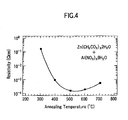
- Figure 4 shows how the resistivity of a thin film formed of a mixture of aluminum nitrate 9-hydrate and ethanol depended on heat treatment (annealing) temperature. It can be seen that setting the heat treatment temperature at around 500°C lowered the resistivity and enabled transformation of organometal molecule thin film to semiconductor thin film.
- Organometals containing oxygen atom include copper acetate, copper formate, copper sulfate, copper chloride, copper nitrate, nickel acetate, nickel formate, nickel sulfate, nickel chloride nickel nitrate, sodium cobalt nitrate, sodium cobalt acetate, sodium cobalt formate, sodium cobalt sulfate, sodium cobalt chloride, sodium nickel nitrate, and their hydrates.
- Doping materials include aluminum nitrate, aluminum acetate, aluminum chloride, aluminum sulfate, aluminum formate, sodium nitrate, sodium acetate, sodium chloride, sodium sulfate, sodium formate, potassium nitrate, potassium acetate, potassium chloride, potassium sulfate, potassium formate, lithium nitrate, lithium acetate, lithium chloride, lithium sulfate, lithium formate, and their hydrates.
- organometal and doping material are dissolved in ethanol or other solvent and thoroughly mixed by stirring to make a p-type organometal material mixed solution.
- a thin film of the mixed solution is formed on a substrate by coating, dipping, spin coating or the like, whereafter the solvent is volatized by drying to produce an organometal molecule thin film on the substrate.
- the same types of substrate can be used as in the case of producing n-type semiconductor.
- the number of repetitions of the coating, dipping or spin coating is controlled to control the thickness of the mixed solution applied to the substrate.
- the organometal molecule thin film formed on the substrate is transformed from the organometal molecule thin film to a p-type metal oxide semiconductor by subsequent heating, decomposition and other chemical reactions.
- the heating temperatures for producing these chemical reactions are, for example, 300 - 1,700°C in the case of copper oxide, 400 - 1,900°C in the case of nickel oxide and 300 - 2,000°C in the case of sodium cobalt oxide.
- a multilayer semiconductor device can be produced by repeating the steps of supplying a predetermined material selected in accordance with the desired semiconductor device structure to form an organometal molecule thin film, heating and decomposing the thin film to obtain a semiconductor thin film, supplying onto the thin film a material for a different thin film, and heating and decomposing the different thin film to obtain a subsequent semiconductor thin film.
- n- and p-type metal oxide semiconductor thin films can be readily produced using a sol-gel process.
- Figure 1 schematically illustrates a sol-gel process utilizing spin coating.
- a mixed solution of n- or p-type organometal material 2 is dripped onto a substrate 1 being rotated at speed of about 100 - 500 rpm.
- the rotating speed after dripping (1,000 - 4,000 rpm) and the viscosity and temperature of the mixed solution are regulated to control the thickness of the so-formed thin film.
- a heater 3 is used to heat it to around 250°C to evaporate its solvent component and then to the temperature cited earlier for causing chemical reaction of the organometal material, thereby heat-treating the film 4 to produce a metal oxide semiconductor thin film.
- a substrate 11 made of glass, ceramic, heat-resistant plastic, metal or the like and formed with metal electrodes is immersed in a p-type organometal material mixed solution 12.
- the mixed solution can be one of those mentioned in the earlier explanation regarding production of p-type semiconductor.
- the substrate 11 After the substrate 11 has been withdrawn from the mixed solution 12 and dried, it is passed through a heater 13 to subject the organometal molecule thin film on the substrate to chemical reaction that transforms it to a metal oxide semiconductor thin film.
- the heating temperature by the heater 13 for causing the chemical reaction is, for example, 300 - 1,700°C when the p-type organometal material is copper oxide, 400 - 1,900°C when it is nickel oxide and 300 - 2,000°C when it is sodium cobalt oxide.
- the substrate 11 bearing the thin film is immersed in an n ⁇ type organometal material mixed solution 14.
- the mixed solution can be one of those mentioned in the earlier explanation regarding production of n-type semiconductor.
- the substrate 11 After the substrate 11 has been withdrawn from the mixed solution 14 and dried, it is heated by a heater 15 to produce a reaction that forms an n-type metal oxide semiconductor thin film 1 in on the p-type metal oxide semiconductor thin film lip. thereby forming a p-n junction structure that constitutes a solar cell.
- the heating temperature by the heater 15 is, for example, 400 - 600°C when the n-type organometal material is zinc oxide, 200 - 400°C when it is indium oxide and 200 - 600°C when it is tin oxide.
- This dip method is an excellent choice for production of solar cells because it enables large-area p-n junction semiconductor to be produced easily, rapidly and inexpensively.
- the coating method which resembles the dip method in the point of being substantially free of coating unevenness, can also be applied using large-area compatible equipment to produce large-area devices easily, rapidly and inexpensively.
- One surface of a substrate 21 formed with metal electrodes is brought opposite an opening of a vapor deposition chamber 23 and a p-type organometal material 22 is heated and vaporized by a heater 24 to vapor-deposit p-type organometal material on the surface of the substrate 21 facing into the deposition chamber 23.
- a heater 25 located above the substrate 21 is used to heat the substrate 21 from behind so as to simultaneously dry and react the vapor-deposited film and form a p-type oxide semiconductor thin film.
- the substrate 21 is moved to bring the p-type oxide semiconductor thin film opposite an opening of a vapor deposition chamber 27 and an n-type organometal material 26 is heated and vaporized by a heater 28 to vapor-deposit n-type organometal material on the p-type oxide semiconductor thin film on the substrate 21.
- a heater 29 located above the substrate 21 is used to heat the substrate 21 from behind so as to simultaneously dry and react the vapor-deposited film and form an n-type oxide semiconductor thin film, thereby establishing a p-n junction structure that constitutes a solar cell.
- the p-type organometal material, n-type organometal material, the heating and reaction conditions and the like are similar to those in the dip method.
- the vapor deposition and heating method effects vapor deposition, drying and reaction of the organic material of the oxide semiconductor simultaneously, it enables production of solar cells at a speed that compares favorably with that of the dip and coating methods.
- Examples 1 and 2 set out below respectively describe a method of producing an n-type semiconductor thin film and a method of producing a p-type semiconductor thin film. It should be noted, however, that the present invention is in no way limited to these Examples.
- Zinc acetate 2-hydrate was used as an organometal containing an oxygen atom, aluminum nitrate 9-hydrate was used as n-type dopant, and ethanol was used as solvent. These were mixed by means of stirring at 80°C for three hours to obtain a transparent mixed solution.
- a ceramic substrate was immersed in the mixed solution, immediately withdrawn and dried at 260°C for 10 minutes.
- an organometal molecule thin film had been formed on the substrate by the foregoing process, it was maintained at about 500°C for 1 hour to form an aluminum-containing zinc oxide thin film constituting an n-type semiconductor.
- aluminum was used as n-type dopant in this Example, it was ascertained that an increase in n-type carriers could also be realized by addition of boron, gallium, indium or the like.
- Copper acetate 1-hydrate was used as an organometal containing an oxygen atom, aluminum nitrate 9-hydrate was used as p-type dopant, and ethanol was used as solvent. These were mixed by means of stirring at 80°C for about three hours to obtain a transparent mixed solution.
- a ceramic substrate was immersed in the mixed solution, immediately withdrawn and dried at 260°C for 10 minutes.
- an organometal molecule thin film had been formed on the substrate in the foregoing manner, it was maintained at about 1,000°C for 1 hour to form an aluminum-containing copper oxide thin film constituting a p-type semiconductor.
- Aluminum was added as a p-type dopant in this Example because it enables a broad light adsorption bandwidth to be achieved in a case where use as the absorption layer of a solar cell is intended when a zinc oxide system n-type layer is used.
- increase in p-type carriers can also be promoted by addition of gallium, strontium or the like.
- an organic molecule having as structural elements both a semiconductor anion atom and cation atom is applied to a substrate by spraying, dipping, spin coating or the like and reacted under heating to obtain p-type and n-type semiconductor thin films whose p-n junctions enable rapid fabrication of large-area semiconductor devices, light-emitting elements and solar cells inexpensively and in high volume.
- the substrate can be metal, ceramic, glass, heat-resistant plastic or any other material able to withstand the heating temperature for reaction
- the invention enables solar cells to be directly fabricated on virtually any type of material, including roofs, walls, etc. of buildings and any of various types of equipment, such as motor vehicles and airplanes.
- the production method according to the present invention is simple and inexpensive. As such, it enables a reduction in the amount of energy consumption required for the fabrication of semiconductor devices and solar cells.
- the semiconductor provided by the invention is oxide semiconductor opens the way to production of a new generation of highly durable solar cells that are excellent in environmental friendliness and energy conservation.
- the method of producing semiconductor according to this invention can be applied for production of large-area light-emitting devices, it can be expected to help reduce electric power consumption for lighting by enabling inexpensive fabrication of large area light-emitting elements.
Landscapes
- Liquid Deposition Of Substances Of Which Semiconductor Devices Are Composed (AREA)
- Photovoltaic Devices (AREA)
Abstract
Description
Claims (13)
- A method of producing a metal oxide semiconductor thin film, characterized in that it comprises at least one step of adhering a mixed solution of an organometal containing an oxygen atom and a solvent to a substrate; and at least one step of decomposing and oxidizing the organometal by heat treatment at a predetermined temperature.
- The method according to claim 1, characterized in that the semiconductor thin film is n-type, that the organometal is zinc acetate, zinc acetylacetonate, zinc formate, zinc hydroxide, zinc chloride, zinc nitrate, or one of their hydrates, and that the method further comprises a step of doping, before the step of adhering, the organometal with aluminum nitrate, aluminum acetate, aluminum chloride, aluminum sulfate, aluminum formate, gallium nitrate, gallium acetate, gallium chloride, gallium sulfate, gallium formate, indium nitrate, indium acetate, indium chloride, indium sulfate, indium formate, boron nitrate, boron acetate, boron chloride, boron sulfate, boron formate, or one of their hydrates.
- The method according to claim 1, characterized in that the semiconductor thin film is p-type, that the organometal is copper acetate, copper formate, copper sulfate, copper chloride, copper nitrate, nickel acetate, nickel formate, nickel sulfate, nickel chloride, nickel nitrate, sodium cobalt nitrate, sodium cobalt acetate, sodium cobalt formate, sodium cobalt sulfate, sodium cobalt chloride, sodium nickel nitrate, or one of their hydrates, and that the method further comprises a step of doping, before the step of adhering, the organometal with aluminum nitrate, aluminum acetate, aluminum chloride, aluminum sulfate, aluminum formate, sodium nitrate, sodium acetate, sodium chloride, sodium sulfate, sodium formate, potassium nitrate, potassium acetate, potassium chloride, potassium sulfate, potassium formate, lithium nitrate, lithium acetate, lithium chloride, lithium sulfate, lithium formate, or one of their hydrates.
- The method according to claim 1, characterized in that the at least one step of adhering comprises a first adhering step in which the organometal contains a p-type impurity and a second adhering step in which the organometal contains an n-type impurity, that the at least one step of decomposing and oxidizing comprises a first heat-treating step to form a p-type oxide semiconductor thin, film and a second heat-treating step to form an n-type oxide semiconductor thin film, and that the first adhering step, first heat-treating step, second adhering step and second heat-treating step are taken in the order mentioned, thereby fabricating a p-n junction.
- The method according to claim 4, characterized in that the organometal containing the p-type impurity is copper acetate, copper formate, copper sulfate, copper chloride, copper nitrate, nickel acetate, nickel formate, nickel sulfate, nickel chloride, nickel nitrate, sodium cobalt nitrate, sodium cobalt acetate, sodium cobalt formate, sodium cobalt sulfate, sodium cobalt chloride, sodium nickel nitrate, or one of their hydrates and is doped with aluminum nitrate, aluminum acetate, aluminum chloride, aluminum sulfate, aluminum formate, sodium nitrate, sodium acetate, sodium chloride, sodium sulfate, sodium formate, potassium nitrate, potassium acetate, potassium chloride, potassium sulfate, potassium formate, lithium nitrate, lithium acetate, lithium chloride, lithium sulfate, lithium formate, or one of their hydrates, and that the organometal containing the n-type impurity is zinc acetate, zinc acetylacetonate, zinc formate, zinc hydroxide, zinc chloride, zinc nitrate, or one of their hydrates and is doped with aluminum nitrate, aluminum acetate, aluminum chloride, aluminum sulfate, aluminum formate, gallium nitrate, gallium acetate, gallium chloride, gallium sulfate, gallium formate, indium nitrate, indium acetate, indium chloride, indium sulfate, indium formate, boron nitrate, boron acetate, boron chloride, boron sulfate, boron formate, or one of their hydrates.
- The method according to claim 1, characterized in that the metal oxide semiconductor thin film is produced utilizing a sol-gel process.
- The method according to claim 1, characterized in that the substrate is made of metal, ceramic, glass or heat-resistant plastic.
- , A metal oxide semiconductor thin film characterized in that it is fabricated by heat-treating a mixed solution of an organometal containing an oxygen atom and an organic solvent adhered to a substrate at a predetermined temperature to decompose and oxidize the organometal.
- The semiconductor thin film according to claim 8, characterized in that the organometal is zinc acetate, zinc acetylacetonate, zinc formate, zinc hydroxide, zinc chloride, zinc nitrate, or one of their hydrates and is doped with aluminum nitrate, aluminum acetate, aluminum chloride, aluminum sulfate, aluminum formate, gallium nitrate, gallium acetate, gallium chloride, gallium sulfate, gallium formate, indium nitrate, indium acetate, indium chloride, indium sulfate, indium formate, boron nitrate, boron acetate, boron chloride, boron sulfate, boron formate, or one of their hydrates.
- The semiconductor thin film according to claim 8, characterized in that the organometal is copper acetate, copper formate, copper sulfate, copper chloride, copper nitrate, nickel acetate, nickel formate, nickel sulfate, nickel chloride, nickel nitrate, sodium cobalt nitrate, sodium cobalt acetate, sodium cobalt formate, sodium cobalt sulfate, sodium cobalt chloride, sodium nickel nitrate, or one of their hydrates and is doped with aluminum nitrate, aluminum acetate, aluminum chloride, aluminum sulfate, aluminum formate, sodium nitrate, sodium acetate, sodium chloride, sodium sulfate, sodium formate, potassium nitrate, potassium acetate, potassium chloride, potassium sulfate, potassium formate, lithium nitrate, lithium acetate, lithium chloride, lithium sulfate, lithium formate, or one of their hydrates.
- The semiconductor thin film according to claim 8, characterized in that it has a p-n junction formed of a p-type oxide semiconductor thin film obtained by heat-processing a mixed solution of an organometal containing a p-type impurity and a solvent adhered to the substrate at a predetermined temperature and an n-type oxide semiconductor thin film formed by adhering a mixed solution of an organometal containing an n-type impurity and a solvent to the thin film and heat-treating the adhered mixed solution at a predetermined temperature.
- The semiconductor thin film according to claim 11, characterized in that the organometal containing the p-type impurity is copper acetate, copper formate, copper sulfate, copper chloride, copper nitrate, nickel acetate, nickel formate, nickel sulfate, nickel chloride, nickel nitrate, sodium cobalt nitrate, sodium cobalt acetate, sodium cobalt formate, sodium cobalt sulfate, sodium cobalt chloride, sodium nickel nitrate, or one of their hydrates and is doped with aluminum nitrate, aluminum acetate, aluminum chloride, aluminum sulfate, aluminum formate, sodium nitrate, sodium acetate, sodium chloride, sodium sulfate, sodium formate, potassium nitrate, potassium acetate, potassium chloride, potassium sulfate, potassium formate, lithium nitrate, lithium acetate, lithium chloride, lithium sulfate, lithium formate, or one of their hydrates, and that the organometal containing the n-type impurity is zinc acetate, zinc acetylacetonate, zinc formate, zinc hydroxide, zinc chloride, zinc nitrate, or one of their hydrates and is doped with aluminum nitrate, aluminum acetate, aluminum chloride, aluminum sulfate, aluminum formate, gallium nitrate, gallium acetate, gallium chloride, gallium sulfate, gallium formate, indium nitrate, indium acetate, indium chloride, indium sulfate, indium formate, boron nitrate, boron acetate, boron chloride, boron sulfate, boron formate, or one of their hydrates.
- The semiconductor thin film according to claim 8, characterized in that the substrate is made of metal, ceramic, glass or heat-resistant plastic.
Applications Claiming Priority (2)
| Application Number | Priority Date | Filing Date | Title |
|---|---|---|---|
| JP2001378118 | 2001-12-12 | ||
| JP2001378118A JP2003179242A (en) | 2001-12-12 | 2001-12-12 | Metal oxide semiconductor thin film and method for producing the same |
Publications (2)
| Publication Number | Publication Date |
|---|---|
| EP1324398A2 true EP1324398A2 (en) | 2003-07-02 |
| EP1324398A3 EP1324398A3 (en) | 2007-05-16 |
Family
ID=19185930
Family Applications (1)
| Application Number | Title | Priority Date | Filing Date |
|---|---|---|---|
| EP02258551A Withdrawn EP1324398A3 (en) | 2001-12-12 | 2002-12-11 | Metal oxide semiconductor thin film and method of producing the same |
Country Status (3)
| Country | Link |
|---|---|
| US (2) | US20030122122A1 (en) |
| EP (1) | EP1324398A3 (en) |
| JP (1) | JP2003179242A (en) |
Cited By (7)
| Publication number | Priority date | Publication date | Assignee | Title |
|---|---|---|---|---|
| WO2006138072A1 (en) * | 2005-06-16 | 2006-12-28 | Eastman Kodak Company | Thin film transistors comprising zinc-oxide-based semiconductor materials |
| WO2006138071A1 (en) * | 2005-06-16 | 2006-12-28 | Eastman Kodak Company | Thin film transistors comprising zinc-oxide-based semiconductor materials |
| WO2007005813A3 (en) * | 2005-07-02 | 2007-05-03 | Hewlett Packard Development Co | Inorganic semiconductive films and methods therefor |
| DE102007043920A1 (en) | 2007-07-17 | 2009-01-22 | Merck Patent Gmbh | Functional material for printed electronic components |
| US7972898B2 (en) * | 2007-09-26 | 2011-07-05 | Eastman Kodak Company | Process for making doped zinc oxide |
| US8441008B2 (en) | 2010-04-28 | 2013-05-14 | Korea Advanced Institute Of Science And Technology | Solution composition for manufacturing metal oxide semiconductor |
| CN104081498A (en) * | 2012-01-27 | 2014-10-01 | 默克专利有限公司 | Method for producing electrically semi-conductive or conductive layers with improved conductivity |
Families Citing this family (26)
| Publication number | Priority date | Publication date | Assignee | Title |
|---|---|---|---|---|
| US20040108505A1 (en) * | 2002-09-16 | 2004-06-10 | Tuller Harry L. | Method for p-type doping wide band gap oxide semiconductors |
| JP2004311845A (en) * | 2003-04-09 | 2004-11-04 | National Institute Of Advanced Industrial & Technology | Visible light transmitting structure with power generation function |
| US7265003B2 (en) * | 2004-10-22 | 2007-09-04 | Hewlett-Packard Development Company, L.P. | Method of forming a transistor having a dual layer dielectric |
| CN100341117C (en) * | 2005-06-09 | 2007-10-03 | 山东师范大学 | Preparation of P-type impurity source and doping technique |
| US7329915B2 (en) * | 2005-11-21 | 2008-02-12 | Hewlett-Packard Development Company, L.P. | Rectifying contact to an n-type oxide material or a substantially insulating oxide material |
| KR101275800B1 (en) * | 2006-04-28 | 2013-06-18 | 삼성전자주식회사 | Non-volatile memory device comprising variable resistance material |
| KR101407298B1 (en) | 2007-11-08 | 2014-06-13 | 연세대학교 산학협력단 | Semiconductor liquid composition and method for producing the same |
| TWI513014B (en) * | 2008-05-19 | 2015-12-11 | Tatung Co | High performance optoelectronic components |
| CN101719493B (en) | 2008-10-08 | 2014-05-14 | 株式会社半导体能源研究所 | Display device |
| TWI388506B (en) * | 2008-12-16 | 2013-03-11 | 財團法人工業技術研究院 | Method for preparing P-type metal oxide semiconductor material |
| RU2527092C2 (en) | 2010-04-02 | 2014-08-27 | Адвенира Энтерпрайзис, Инк. | Coat applicator appliance |
| CN102933496B (en) * | 2010-06-08 | 2014-10-22 | 住友金属矿山株式会社 | Method for producing metal oxide film, metal oxide film, element using the metal oxide film, substrate with metal oxide film, and device using the substrate with metal oxide film |
| EP2534673B1 (en) | 2010-09-13 | 2015-02-18 | Panasonic Corporation | Method for manufacturing a metal oxide semiconductor |
| TWI412082B (en) * | 2011-03-07 | 2013-10-11 | Univ Ishou | A manufacturing method of plating film solution for preparing transparent electric conduction film |
| KR101850510B1 (en) | 2011-03-22 | 2018-04-20 | 삼성디스플레이 주식회사 | precursor composition for oxide semiconductor and manufacturing method of thin film transistor array panel using the same |
| RU2604631C1 (en) | 2011-05-26 | 2016-12-10 | Адвенира Энтерпрайзис, Инк. | Method of applying coating onto object |
| KR101333316B1 (en) | 2012-02-17 | 2013-11-27 | 연세대학교 산학협력단 | Metal oxide thin film, preparation method thereof, and solution for the same |
| JP2014027263A (en) | 2012-06-15 | 2014-02-06 | Semiconductor Energy Lab Co Ltd | Semiconductor device and manufacturing method of the same |
| US9245958B2 (en) | 2012-08-10 | 2016-01-26 | Semiconductor Energy Laboratory Co., Ltd. | Semiconductor device and method for manufacturing the same |
| TWI495615B (en) | 2012-09-28 | 2015-08-11 | 財團法人工業技術研究院 | P-type metal oxide semiconductor material |
| KR20140078543A (en) * | 2012-12-14 | 2014-06-25 | 한국화학연구원 | Indium zinc oxide semiconductor ink composition generating self-combustion reaction and the inorganic semiconductor film thereof |
| JP6341372B2 (en) * | 2013-07-18 | 2018-06-13 | 日産化学工業株式会社 | Precursor composition for forming metal oxide semiconductor layer and method for producing metal oxide semiconductor layer |
| EP3151289A1 (en) * | 2015-10-01 | 2017-04-05 | LG Electronics Inc. | Solar cell |
| TWI566417B (en) | 2015-12-04 | 2017-01-11 | 財團法人工業技術研究院 | P-type metal oxide semiconductor material and transistor |
| CN106784035B (en) * | 2016-12-21 | 2018-01-12 | 浙江海洋大学 | A kind of ZnO antireflection films and its film plating process for silicon solar cell |
| PL439040A1 (en) * | 2021-09-27 | 2023-04-03 | Centrum Badań I Rozwoju Technologii Dla Przemysłu Spółka Akcyjna | Doping solution, method of preparing a layer doped with atoms of at least one metal m selected from group 1 or 2 of the periodic table with the properties of a p-type semiconductor containing copper oxide and/or oxides in oxidation state i or ii, a doped layer, use of such a layer for construction of a photovoltaic cell, and a photovoltaic cell comprising such a layer |
Family Cites Families (5)
| Publication number | Priority date | Publication date | Assignee | Title |
|---|---|---|---|---|
| US5180686A (en) * | 1988-10-31 | 1993-01-19 | Energy Conversion Devices, Inc. | Method for continuously deposting a transparent oxide material by chemical pyrolysis |
| EP0837511B1 (en) * | 1996-10-15 | 2005-09-14 | Matsushita Electric Industrial Co., Ltd | Solar cell and method for manufacturing the same |
| JP2001156321A (en) * | 1999-03-09 | 2001-06-08 | Fuji Xerox Co Ltd | Semiconductor device and method of manufacturing the same |
| JP4055334B2 (en) * | 2000-06-13 | 2008-03-05 | ソニー株式会社 | Manufacturing method of semiconductor device |
| US6946597B2 (en) * | 2002-06-22 | 2005-09-20 | Nanosular, Inc. | Photovoltaic devices fabricated by growth from porous template |
-
2001
- 2001-12-12 JP JP2001378118A patent/JP2003179242A/en active Pending
-
2002
- 2002-12-11 EP EP02258551A patent/EP1324398A3/en not_active Withdrawn
- 2002-12-12 US US10/316,824 patent/US20030122122A1/en not_active Abandoned
-
2005
- 2005-02-08 US US11/052,082 patent/US20050130844A1/en not_active Abandoned
Cited By (12)
| Publication number | Priority date | Publication date | Assignee | Title |
|---|---|---|---|---|
| WO2006138072A1 (en) * | 2005-06-16 | 2006-12-28 | Eastman Kodak Company | Thin film transistors comprising zinc-oxide-based semiconductor materials |
| WO2006138071A1 (en) * | 2005-06-16 | 2006-12-28 | Eastman Kodak Company | Thin film transistors comprising zinc-oxide-based semiconductor materials |
| US7402506B2 (en) | 2005-06-16 | 2008-07-22 | Eastman Kodak Company | Methods of making thin film transistors comprising zinc-oxide-based semiconductor materials and transistors made thereby |
| US7691666B2 (en) | 2005-06-16 | 2010-04-06 | Eastman Kodak Company | Methods of making thin film transistors comprising zinc-oxide-based semiconductor materials and transistors made thereby |
| WO2007005813A3 (en) * | 2005-07-02 | 2007-05-03 | Hewlett Packard Development Co | Inorganic semiconductive films and methods therefor |
| US7695998B2 (en) | 2005-07-02 | 2010-04-13 | Hewlett-Packard Development Company, L.P. | Methods for making and using high-mobility inorganic semiconductive films |
| DE102007043920A1 (en) | 2007-07-17 | 2009-01-22 | Merck Patent Gmbh | Functional material for printed electronic components |
| US8367461B2 (en) | 2007-07-17 | 2013-02-05 | Merck Patent Gmbh | Functional material for printed electronic components |
| US7972898B2 (en) * | 2007-09-26 | 2011-07-05 | Eastman Kodak Company | Process for making doped zinc oxide |
| US8441008B2 (en) | 2010-04-28 | 2013-05-14 | Korea Advanced Institute Of Science And Technology | Solution composition for manufacturing metal oxide semiconductor |
| KR101265227B1 (en) | 2010-04-28 | 2013-05-24 | 한국과학기술원 | Solution composition for manufacturing metal oxide semiconductor |
| CN104081498A (en) * | 2012-01-27 | 2014-10-01 | 默克专利有限公司 | Method for producing electrically semi-conductive or conductive layers with improved conductivity |
Also Published As
| Publication number | Publication date |
|---|---|
| US20050130844A1 (en) | 2005-06-16 |
| EP1324398A3 (en) | 2007-05-16 |
| JP2003179242A (en) | 2003-06-27 |
| US20030122122A1 (en) | 2003-07-03 |
Similar Documents
| Publication | Publication Date | Title |
|---|---|---|
| US20030122122A1 (en) | Metal oxide semiconductor thin film and method of producing the same | |
| Jeong et al. | Low-temperature, solution-processed metal oxide thin film transistors | |
| Chopra et al. | Chemical solution deposition of inorganic films | |
| US7094651B2 (en) | Hydrazine-free solution deposition of chalcogenide films | |
| CN100490205C (en) | Method for depositing metal sulfur family film and method for preparing field effect transistor | |
| KR100876947B1 (en) | Liquid phase manufacturing method for oxide thin film | |
| US9236157B2 (en) | Transparent electrically conducting oxides | |
| US8932495B1 (en) | Transparent conductor materials and processes for forming such materials | |
| CN111051560B (en) | Method for producing a film of light-absorbing material having a perovskite-like structure | |
| CN105185847A (en) | Method for preparing copper-zinc-tin-sulfur film | |
| US10453988B2 (en) | Methods for creating cadmium telluride (CdTe) and related alloy film | |
| US20060057766A1 (en) | Method for preparation of semiconductive films | |
| TWI552198B (en) | Modification of the ruthenium layer from the decane-containing blend | |
| KR100621447B1 (en) | Solution deposition of chalcogenide film and preparation of field effect transistor comprising chalcogenide film | |
| JP2005223231A (en) | Method for producing metal oxide semiconductor thin film and metal oxide semiconductor thin film | |
| Caram et al. | Analysis of substrate coverage of hybrid halide perovskite thin films deposited on glass | |
| CN101445513B (en) | Metal oxide coatings | |
| CN106521415B (en) | An improved annealing method for indium oxide transparent conductive films | |
| Khalilzadeh-Rezaie et al. | Optical and electrical properties of tin oxide-based thin films prepared by streaming process for electrodeless electrochemical deposition | |
| CN110255603B (en) | A method for uniform sodium doping of CuInS2 thin films | |
| CN113571406A (en) | A kind of method for preparing antimony selenium sulfide thin film by liquid phase selenization | |
| Khalilzadeh-Rezaie et al. | Fluorine-doped tin oxide thin films grown by streaming process for electrodeless electrochemical deposition | |
| Huang et al. | Conducting and Optical Properties of Transparent Conducting Indium-Doped Zinc Oxide Thin Films by Sol-Gel Processing | |
| Tracey | Dye sensitisation of sol-gel derived titanium dioxide films |
Legal Events
| Date | Code | Title | Description |
|---|---|---|---|
| PUAI | Public reference made under article 153(3) epc to a published international application that has entered the european phase |
Free format text: ORIGINAL CODE: 0009012 |
|
| AK | Designated contracting states |
Designated state(s): AT BE BG CH CY CZ DE DK EE ES FI FR GB GR IE IT LI LU MC NL PT SE SI SK TR |
|
| AX | Request for extension of the european patent |
Extension state: AL LT LV MK RO |
|
| PUAL | Search report despatched |
Free format text: ORIGINAL CODE: 0009013 |
|
| AK | Designated contracting states |
Kind code of ref document: A3 Designated state(s): AT BE BG CH CY CZ DE DK EE ES FI FR GB GR IE IT LI LU MC NL PT SE SI SK TR |
|
| AX | Request for extension of the european patent |
Extension state: AL LT LV MK RO |
|
| AKX | Designation fees paid | ||
| REG | Reference to a national code |
Ref country code: DE Ref legal event code: 8566 |
|
| STAA | Information on the status of an ep patent application or granted ep patent |
Free format text: STATUS: THE APPLICATION IS DEEMED TO BE WITHDRAWN |
|
| 18D | Application deemed to be withdrawn |
Effective date: 20071117 |