EP1324393A1 - Manufacturing process of a semiconductor non-volatile memory cell and corresponding memory-cell - Google Patents
Manufacturing process of a semiconductor non-volatile memory cell and corresponding memory-cell Download PDFInfo
- Publication number
- EP1324393A1 EP1324393A1 EP02014408A EP02014408A EP1324393A1 EP 1324393 A1 EP1324393 A1 EP 1324393A1 EP 02014408 A EP02014408 A EP 02014408A EP 02014408 A EP02014408 A EP 02014408A EP 1324393 A1 EP1324393 A1 EP 1324393A1
- Authority
- EP
- European Patent Office
- Prior art keywords
- layer
- dielectric layer
- cell according
- memory cell
- volatile memory
- Prior art date
- Legal status (The legal status is an assumption and is not a legal conclusion. Google has not performed a legal analysis and makes no representation as to the accuracy of the status listed.)
- Granted
Links
Images


Classifications
-
- H—ELECTRICITY
- H10—SEMICONDUCTOR DEVICES; ELECTRIC SOLID-STATE DEVICES NOT OTHERWISE PROVIDED FOR
- H10D—INORGANIC ELECTRIC SEMICONDUCTOR DEVICES
- H10D64/00—Electrodes of devices having potential barriers
- H10D64/01—Manufacture or treatment
- H10D64/013—Manufacture or treatment of electrodes having a conductor capacitively coupled to a semiconductor by an insulator
- H10D64/01302—Manufacture or treatment of electrodes having a conductor capacitively coupled to a semiconductor by an insulator the insulator being formed after the semiconductor body, the semiconductor being silicon
- H10D64/01332—Making the insulator
- H10D64/01336—Making the insulator on single crystalline silicon, e.g. chemical oxidation using a liquid
- H10D64/0134—Making the insulator on single crystalline silicon, e.g. chemical oxidation using a liquid with a treatment, e.g. annealing, after the formation of the insulator and before the formation of the conductor
-
- H—ELECTRICITY
- H10—SEMICONDUCTOR DEVICES; ELECTRIC SOLID-STATE DEVICES NOT OTHERWISE PROVIDED FOR
- H10D—INORGANIC ELECTRIC SEMICONDUCTOR DEVICES
- H10D64/00—Electrodes of devices having potential barriers
- H10D64/01—Manufacture or treatment
- H10D64/013—Manufacture or treatment of electrodes having a conductor capacitively coupled to a semiconductor by an insulator
- H10D64/01302—Manufacture or treatment of electrodes having a conductor capacitively coupled to a semiconductor by an insulator the insulator being formed after the semiconductor body, the semiconductor being silicon
- H10D64/01332—Making the insulator
- H10D64/01336—Making the insulator on single crystalline silicon, e.g. chemical oxidation using a liquid
- H10D64/01342—Making the insulator on single crystalline silicon, e.g. chemical oxidation using a liquid by deposition, e.g. evaporation, ALD or laser deposition
-
- H—ELECTRICITY
- H10—SEMICONDUCTOR DEVICES; ELECTRIC SOLID-STATE DEVICES NOT OTHERWISE PROVIDED FOR
- H10D—INORGANIC ELECTRIC SEMICONDUCTOR DEVICES
- H10D64/00—Electrodes of devices having potential barriers
- H10D64/01—Manufacture or treatment
- H10D64/013—Manufacture or treatment of electrodes having a conductor capacitively coupled to a semiconductor by an insulator
- H10D64/01302—Manufacture or treatment of electrodes having a conductor capacitively coupled to a semiconductor by an insulator the insulator being formed after the semiconductor body, the semiconductor being silicon
- H10D64/01332—Making the insulator
- H10D64/01336—Making the insulator on single crystalline silicon, e.g. chemical oxidation using a liquid
- H10D64/01344—Making the insulator on single crystalline silicon, e.g. chemical oxidation using a liquid in a nitrogen-containing ambient, e.g. N2O oxidation
-
- H—ELECTRICITY
- H10—SEMICONDUCTOR DEVICES; ELECTRIC SOLID-STATE DEVICES NOT OTHERWISE PROVIDED FOR
- H10D—INORGANIC ELECTRIC SEMICONDUCTOR DEVICES
- H10D64/00—Electrodes of devices having potential barriers
- H10D64/60—Electrodes characterised by their materials
- H10D64/66—Electrodes having a conductor capacitively coupled to a semiconductor by an insulator, e.g. MIS electrodes
- H10D64/68—Electrodes having a conductor capacitively coupled to a semiconductor by an insulator, e.g. MIS electrodes characterised by the insulator, e.g. by the gate insulator
- H10D64/681—Electrodes having a conductor capacitively coupled to a semiconductor by an insulator, e.g. MIS electrodes characterised by the insulator, e.g. by the gate insulator having a compositional variation, e.g. multilayered
- H10D64/685—Electrodes having a conductor capacitively coupled to a semiconductor by an insulator, e.g. MIS electrodes characterised by the insulator, e.g. by the gate insulator having a compositional variation, e.g. multilayered being perpendicular to the channel plane
-
- H—ELECTRICITY
- H10—SEMICONDUCTOR DEVICES; ELECTRIC SOLID-STATE DEVICES NOT OTHERWISE PROVIDED FOR
- H10D—INORGANIC ELECTRIC SEMICONDUCTOR DEVICES
- H10D64/00—Electrodes of devices having potential barriers
- H10D64/60—Electrodes characterised by their materials
- H10D64/66—Electrodes having a conductor capacitively coupled to a semiconductor by an insulator, e.g. MIS electrodes
- H10D64/68—Electrodes having a conductor capacitively coupled to a semiconductor by an insulator, e.g. MIS electrodes characterised by the insulator, e.g. by the gate insulator
- H10D64/693—Electrodes having a conductor capacitively coupled to a semiconductor by an insulator, e.g. MIS electrodes characterised by the insulator, e.g. by the gate insulator the insulator comprising nitrogen, e.g. nitrides, oxynitrides or nitrogen-doped materials
-
- H—ELECTRICITY
- H10—SEMICONDUCTOR DEVICES; ELECTRIC SOLID-STATE DEVICES NOT OTHERWISE PROVIDED FOR
- H10D—INORGANIC ELECTRIC SEMICONDUCTOR DEVICES
- H10D64/00—Electrodes of devices having potential barriers
- H10D64/60—Electrodes characterised by their materials
- H10D64/66—Electrodes having a conductor capacitively coupled to a semiconductor by an insulator, e.g. MIS electrodes
- H10D64/68—Electrodes having a conductor capacitively coupled to a semiconductor by an insulator, e.g. MIS electrodes characterised by the insulator, e.g. by the gate insulator
- H10D64/691—Electrodes having a conductor capacitively coupled to a semiconductor by an insulator, e.g. MIS electrodes characterised by the insulator, e.g. by the gate insulator comprising metallic compounds, e.g. metal oxides or metal silicates
Definitions
- the present invention relates to a manufacturing process of a semiconductor non-volatile memory cell, and corresponding memory cell.
- the invention relates specifically to a manufacturing process of a non-volatile memory cell, being integrated in a semiconductor substrate and having a gate region comprising a floating gate region and a control gate region, which process comprises the steps of:
- the invention also relates to a memory cell, being integrated in a semiconductor substrate, comprising at least a source region and a drain region separated by a channel region, and having a gate region formed in said channel region, which gate region is isolated from said semiconductor substrate by a first dielectric layer formed on said semiconductor substrate, said gate region comprising a floating gate region and a control gate region that are isolated from each other by an interpoly dielectric layer, with said floating gate region comprising a semiconductor layer.
- the invention applies to the manufacture of semiconductor memory devices, such as non-volatile flash EEPROMs (Electrically Erasable/Programmable Read Only Memories).
- flash EEPROMs can be erased with a single operation performed simultaneously on all the memory cells.
- the invention applies to the manufacture of a non-volatile memory cell, e.g. of the flash EEPROM type, having an interpoly dielectric layer of reduced electrical thickness, for a given number of interpoly dielectric layers as provided in the state of the art, and it ensures proper performance of the device as regards its electrical characteristics and retention of a logic state programmed in it.
- a non-volatile memory cell e.g. of the flash EEPROM type
- the invention further relates to a process for manufacturing, either to a very large integration scale or single wafer scale, flash EEPROM non-volatile memory devices exhibiting the above features.
- re-programmable non-volatile memory cells integrated in a semiconductor substrate comprise a floating gate FET (Field-Effect Transistor), and an interpoly dielectric layer provided between the floating gate region and the control gate region to function as an insulator layer of charges stored into the floating gate region.
- FET Field-Effect Transistor
- interpoly dielectric layer provided between the floating gate region and the control gate region to function as an insulator layer of charges stored into the floating gate region.
- the absence or presence of charges in the floating gate region sets the logic state of the memory cell, usually by a binary code of 0 or 1.
- the interpoly dielectric layer can be formed from different materials in a number of different ways.
- a common technique is that of successively depositing three dielectric layers onto the floating gate region, the latter being comprised conventionally of an amorphous or polycrystalline silicon layer (polysilicon layer) deposited onto a thin layer of silicon oxide, known as the tunnel oxide, to isolate the gate region from the semiconductor substrate.
- the resulting stack dielectric layer usually comprises a first silicon oxide layer, a second silicon nitride layer, and a third silicon oxide layer.
- the resulting dielectric is known by the ONO acronym (Oxide Nitride Oxide), or as the interpoly ONO dielectric.
- the nitride layer is used to promote the integration of the three-stack layer to the device process flow.
- the interpoly dielectric forming step is followed by treatments with oxidising species (O 2 , O, OH, H 2 O).
- the nitride layer is impervious to said oxidising species, and is therefore used as a barrier to stop them from diffusing through to the floating gate region.
- the nitride layer prevents further oxidation of the floating gate region and consequent alteration of the interpoly dielectric layer thickness during subsequent device manufacturing steps.
- a single silicon oxide layer single oxide interpoly may be used instead of the ONO layer.
- the thickness of the interpoly dielectric layer is co-responsible, irrespective of its composition and manufacturing method, for the capacitive coupling of the memory cell. Thus, additionally to retaining the logic state over time, it contributes to set the program and erase parameters.
- the underlying technical problem of this invention is to provide a memory cell manufacturing process, whereby the EOT (Equivalent Oxide Thickness) of the dielectric layer between the floating gate and control gate regions can be reduced maintaining the same fisic thickness, and good capacitive coupling of the floating and control gate regions achieved.
- EOT Equivalent Oxide Thickness
- the resolvent idea of this invention is to provide the dielectric layer between the floating and control gate regions as a layer having a high dielectric constant value.
- this dielectric layer having a high dielectric constant value is formed by conventional and unconventional deposition techniques for non-volatile memories.
- this dielectric layer having a high dielectric constant value For easier process integration and improved electric properties of this dielectric layer having a high dielectric constant value, additional dielectric layers are deposited, between this layer having a high dielectric constant value and the floating and control gate regions.
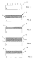
- a gate region of a non-volatile memory cell during a sequence of processing steps according to this invention is shown generally at 10 in schematic form.
- a non-volatile memory cell integrated in a semiconductor substrate comprises source and drain regions that are formed in the semiconductor substrate and separated from each other by a channel region on which a gate region is formed.
- the gate region is isolated from the semiconductor substrate by an oxide layer known as the tunnel oxide.
- the gate region consists of a first region, being the floating gate region, and a second region, being the control gate region, which regions are isolated from each other by a dielectric layer known as the interpoly dielectric.
- This invention concerns the formation of the gate region 10.
- the floating gate region is then defined conventionally in the polysilicon layer 1 by exposing a mask of a photo-sensitive material, and subsequently etching away the polysilicon layer 1, this being followed by removal of the mask of photo-sensitive material.
- a treatment for cleaning the surface of said polysilicon layer 1 with chemical solution is provided.
- the treatment is provided with chemical solution, using either aqueous solutions to form a layer of native oxide, not shown, over the polysilicon layer, or chemical treatment with hydrofluoric acid to passivate the surface of the polysilicon layer 1 with Si-H terminations, e.g. in a HF-last process.
- the treatment comprising hydrofluoric acid is additivated chelate agents, in liquid or vapor phase, to provide a cleaner surface of the polysilicon layer 1.
- interpoly dielectric layer 11 is formed over the floating gate region.
- the interpoly dielectric layer 11 comprises a layer 5 having a high dielectric constant.
- the dielectric layer 5 with a high dielectric constant is a layer having a higher dielectric constant than 10.
- the dielectric layer 5 with a high dielectric constant is formed by a single layer of metal aluminate MAl x O y or of metal silicate (MSi x O y ), for example.
- the dielectric layer 5 comprises transition metal compounds, e.g. of hafnium or zirconium.
- the layer 5 with a high dielectric constant is a stack layer, also known as nano-laminate, comprising a stack of very thin layers (e.g. less than 25 Angstroms thick) of identical or different materials whose dielectric constant is higher than or equal to 3.9.
- the resulting layer 5 has a higher dielectric constant than 10.
- the dielectric layer 5 with a high dielectric constant is deposited by ALCVD (Atomic Layer Chemical Vapor Deposition), MOCVD (Metal-Organic Chemical Vapor Deposition), LPCVD (Low-Pressure Chemical Vapor Deposition), PECVD (Plasma-Enhanced Chemical Vapor Deposition), or using PVD (Physical Vapor Deposition) or MBE (Molecular Beam Epitaxy) techniques, in either batch or single-wafer systems.
- ALCVD Al-Organic Chemical Vapor Deposition
- MOCVD Metal-Organic Chemical Vapor Deposition
- LPCVD Low-Pressure Chemical Vapor Deposition
- PECVD Pasma-Enhanced Chemical Vapor Deposition
- PVD Physical Vapor Deposition
- MBE Molecular Beam Epitaxy
- the thickness of the dielectric layer 5 is selected between 0.5 and 14 nm, as measured in terms of EOT equivalent electrical thickness.
- the physical thickness of the dielectric layer 5, e.g. with a dielectric constant of 10, would range between 1.2 and 36 nm.
- the layer 5 is densified by thermal treatment (using either nitrogen or steam or oxygen, N 2 or H 2 O or O 2 ), in either batch or single-wafer systems.
- the gate region 10 of the memory cell is then finished conventionally by forming the control gate region in the dielectric layer 5.
- This control gate region is formed as a second layer of a semiconductor material such as polysilicon, not shown.
- FIG. 3 A second embodiment according to the invention is shown in Figures 3 and 4.
- the interpoly dielectric layer 11 comprises the dielectric layer 5 with a high dielectric constant and another dielectric layer 3, known as the bottom dielectric.
- the bottom dielectric layer 3 is to isolate the dielectric layer 5 having a high dielectric constant from the floating gate region 1.
- the bottom dielectric layer 3 is silicon dioxide, or a layer of a dielectric material whose dielectric constant is comprised in the range of 3.9 to 10.
- the thickness of the bottom dielectric layer 3 can be selected in the range of 0.5 to 6.0 nm, it being understood that such values are measured in terms of EOT (Equivalent Oxide Thickness).
- the bottom dielectric layer 3 is an alumina layer, Al 2 O 3 , whose dielectric constant is comprised in the 9 to 10 range.
- the bottom dielectric layer 3 is CVD formed in either batch or single-wafer systems.
- the gate region 10 of the memory cell is then finished conventionally by forming the control gate region in the dielectric layer 5.
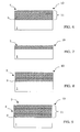
- FIG. 5 A third embodiment according to the invention is shown in Figures 5 and 6.
- the interpoly dielectric layer 11 comprises the dielectric layer 5 with a high dielectric constant and an additional dielectric layer 7, known as the top dielectric.
- the dielectric layer 5 with a high dielectric constant is formed over the polysilicon layer 1, and the top dielectric layer 7 is then formed over the dielectric layer 5 having a high dielectric constant.
- the top dielectric layer 7 may be a silicon dioxide layer or a layer of a dielectric material whose dielectric constant lies in the range of 3.9 to 10.
- the thickness of the top dielectric layer 7 can be selected in the range of 0.5 to 10 nm, it being understood that such values are measured in terms of EOT.
- the top dielectric layer 7 is a layer of aluminum oxide or alumina, Al 2 O 3 , having a dielectric constant in the 8 to 10 range.
- the top dielectric layer 7 is CVD formed in either batch or single-wafer systems.
- the top dielectric layer 7 is then densified by thermal treatment (using either nitrogen or steam or oxygen, N 2 or H 2 O or O 2 ).
- the gate region 10 of the memory cell is then finished conventionally by forming the control gate region in the dielectric layer 7.
- a fourth embodiment according to the invention is shown in Figures 7 to 9.
- the interpoly dielectric layer 11 comprises of the bottom dielectric layer 3 and the top dielectric layer 7.
- the dielectric layer 5 with a high dielectric constant is advantageously encapsulated between said layers.
- the surface interfacing the dielectric layer 5 having a high dielectric constant with the semiconductor layers that form the gate region 10 can be advantageously improved.
- the gate region 10 of the memory cell is then finished conventionally by forming the control gate region in the dielectric layer 7.
- a fifth embodiment of the gate region 10 according to the invention is shown in Figures 10 to 17.
- the interpoly dielectric layer 11 comprises a barrier layer, such as a layer of silicon nitride.
- This barrier layer is formed either in the floating gate region or over one of the layers that comprise the interpoly dielectric layer 11, as described in detail herein below.
- a layer 2 of silicon nitride is formed over the polysilicon layer 1 in the embodiment of Figure 10.
- This layer 2 can be formed by LPCVD (Low-Pressure Chemical Vapor Deposition), RTCVD (Rapid Thermal Chemical Vapor Deposition), PECVD (Plasma-Enhanced Chemical Vapor Deposition), or by directly nitriding the surface (as by plasma or thermal nitriding) in either batch or single-wafer systems.
- the silicon nitride layer 2 functions to inhibit diffusion of any oxidising species (O 2 , O, OH, H 2 O), as may be present in the gas mixtures employed for subsequent thermal treatments to the step of forming the interpoly dielectric layer.
- any oxidising species O 2 , O, OH, H 2 O
- Such oxidising species can also originate from the subsequent process of forming, and optionally densifying, the interpoly dielectric layers.
- the nitride layer 2 is provided as a very thin layer (e.g. about 3 nm thick) in order to keep the overall thickness of the interpoly dielectric layer 11 low.
- the interpoly dielectric layer 11 is formed over the nitride layer 2.
- a bottom dielectric layer 3 is then formed over the nitride layer 2.
- the bottom dielectric layer 3 is advantageously formed as in the embodiment of Figure 3.
- an ultra-thin layer 4 of silicon nitride is now formed over the bottom dielectric layer 3, as shown in Figure 13.
- This layer 4 of silicon nitride may be formed in the same way as the previous layer 2 of silicon nitride.
- a dielectric layer 5 having a high dielectric constant, in particular higher than 10, is formed over the ultra-thin nitride layer 4.
- This dielectric layer 5 with a high dielectric constant has the same characteristics as the dielectric layer 5 with a high dielectric constant of the previously described embodiments, and may be densified as in the embodiment of Figure 2.
- the gate region 10 of the memory cell according to the invention is formed by depositing an ultra-thin layer 6 of silicon nitride onto said dielectric layer 5 with a high dielectric constant, as shown in Figure 15.
- This layer 6 of silicon nitride may be formed the same way as the silicon nitride layers 2 and 4 previously described.
- a top dielectric layer 7 is then formed over the ultra-thin layer 6, if the ultra-thin layer 6 is provided.
- the top dielectric layer 7 may be a layer of silicon dioxide or a layer of a dielectric material whose dielectric constant value is in the range of 3.9 to 10.
- the interpoly dielectric layer 11 is thus completed.
- the top dielectric layer 7 is advantageously formed as in the embodiment of Figure 6.
- an ultra-thin layer 8 of silicon nitride is now deposited onto the top dielectric layer 7, as shown in Figure 17.
- This layer 8 of silicon nitride may be formed in the same way as the silicon nitride layers 2, 4, 6 previously described.
- this ultra-thin layer 8 of silicon nitride is densified by thermal treatment (using either nitrogen or steam or oxygen, N 2 or H 2 O or O 2 ).
- the gate region 10 of the memory cell is then finished conventionally by forming the control gate region in the interpoly dielectric layer 11.
- the process of this invention allows reduced equivalent electrical thickness dimensions of the interpoly dielectric layer 11 to be achieved, with the overall thickness of the latter unchanged or increased, using high dielectric constant layers.
- This allows an electrical thickness of up to 5 equivalent nanometers, i.e. 50 nm technologies, to be achieved.
- the selection of the relative thickness of the dielectric layers 3, 5, 7, comprising the proposed stack construction for the interpoly dielectric layer 11 of the gate region 10, is made more flexible and modular.
Landscapes
- Non-Volatile Memory (AREA)
- Semiconductor Memories (AREA)
Abstract
Description
- depositing a first dielectric layer onto said semiconductor substrate;
- depositing a first semiconductor layer onto said first dielectric layer to form said floating gate region of said gate region; and
- defining said floating gate region of said gate region in said first semiconductor layer.
Claims (34)
- A process for manufacturing a non-volatile memory cell, being integrated in a semiconductor substrate and having a gate region (10) comprised of a floating gate region and a control gate region, the process comprising the steps of:characterized in that it further comprises the step of:depositing a first dielectric layer onto said semiconductor substrate;depositing a first semiconductor layer (1) onto said first dielectric layer to form said floating gate region of said gate region (10); anddefining said floating gate region of said gate region (10) in said first semiconductor layer (1);depositing a second dielectric layer (5), having a higher dielectric constant than 10, onto said first semiconductor layer (1).
- A process for manufacturing a non-volatile memory cell according to Claim 1, characterized in that it comprises the following step:depositing a third layer (3) of dielectric layer between said first semiconductor layer (1) and said second dielectric layer (5).
- A process for manufacturing a non-volatile memory cell according to either Claim 1 or 2, characterized in that it comprises the following step:depositing a fourth layer (7) of dielectric layer onto said second dielectric layer (5).
- A process for manufacturing a non-volatile memory cell according to Claim 1, characterized in that said second dielectric layer (5) is a single layer of a metal aluminate (MAlxOy).
- A process for manufacturing a non-volatile memory cell according to Claim 1, characterized in that said second dielectric layer (5) is a single layer of a metal silicate (MSixOy).
- A process for manufacturing a non-volatile memory cell according to either Claim 4 or 5, characterized in that said dielectric layer (5) comprises transition metals.
- A process for manufacturing a non-volatile memory cell according to Claim 6, characterized in that said transition metals are hafnium or zirconium.
- A process for manufacturing a non-volatile memory cell according to Claim 1, characterized in that said second dielectric layer (5) consists of plurality of layers of different materials having a dielectric constant higher than or equal to 3.9.
- A process for manufacturing a non-volatile memory cell according to Claim 1, characterized in that said second dielectric layer (5) is formed by a CVD (Chemical Vapor Deposition) technique.
- A process for manufacturing a non-volatile memory cell according to Claim 1, characterized in that said second dielectric layer (5) is formed by a PVD (Physical Chemical Deposition) technique.
- A process for manufacturing a non-volatile memory cell according to Claim 1, characterized in that said second dielectric layer (5) is formed by an MBE (Molecular Beam Epitaxy) deposition technique.
- A process for manufacturing a non-volatile memory cell according to either Claim 2 or 3, characterized in that the dielectric constant of said third (3) and fourth (7) dielectric layers is in the range of 3.9 to 10.
- A process for manufacturing a non-volatile memory cell according to either Claim 2 or 3, characterized in that said third (3) and fourth (7) dielectric layers comprise a layer of aluminum oxide.
- A process for manufacturing a non-volatile memory cell according to either Claim 2 or 3, characterized in that said third (3) and fourth (7) dielectric layers are formed by a CVD (Chemical Vapor Deposition) technique.
- A process for manufacturing a non-volatile memory cell according to Claim 1, characterized in that a barrier layer (2) is formed over said first semiconductor layer (1).
- A process for manufacturing a non-volatile memory cell according to Claim 2, characterized in that a barrier layer (4) is formed over said third dielectric layer (3).
- A process for manufacturing a non-volatile memory cell according to Claim 1, characterized in that a barrier layer (6) is formed over said second dielectric layer (5).
- A process for manufacturing a non-volatile memory cell according to Claim 3, characterized in that a barrier layer (8) is formed over said fourth dielectric layer (7).
- A process for manufacturing a non-volatile memory cell according to any of Claims 15 to 18, characterized in that said barrier layer (2,4,6,8) is a layer of silicon nitride.
- A process for manufacturing a non-volatile memory cell according to Claim 19, characterized in that said silicon nitride layer (2,4,6,8) is formed by a CVD (Chemical Vapor Deposition) technique.
- A process for manufacturing a non-volatile memory cell according to Claim 19, characterized in that said silicon nitride layer (2,4,6,8) is formed by direct surface nitriding (using a plasma or a thermal nitriding technique).
- A process for manufacturing a non-volatile memory cell according to either Claim 1 or 3, characterized in that said second (5) and fourth (7) dielectric layers are subjected to densifying treatment.
- A memory cell integrated in a semiconductor substrate having at least a source region and a drain region separated by a channel region, and having a gate region (10) formed on said channel region and isolated from said semiconductor substrate by a first dielectric layer formed on said semiconductor substrate, said gate region (10) comprising a floating gate region and a control gate region that are isolated from each other by an interpoly dielectric layer (11), with said floating gate region (10) comprising a semiconductor layer (1); characterized in that said interpoly dielectric layer (11) comprises a second dielectric layer (5) having a higher dielectric constant than 10.
- A cell according to Claim 23, characterized in that said interpoly dielectric layer (11) comprises a third dielectric layer (3) intervening between said second dielectric layer (5) and said first semiconductor layer (1).
- A cell according to either Claim 23 or 24, characterized in that said interpoly dielectric layer (11) comprises a fourth dielectric layer (7) formed over said second dielectric layer (5).
- A cell according to Claim 23, characterized in that said second dielectric layer (5) is a single layer of a metal aluminate (MAlxOy).
- A cell according to Claim 23, characterized in that said second dielectric layer (5) is a single layer of a metal silicate (MSixOy).
- A cell according to either Claim 26 or 27, characterized in that said dielectric layer (5) comprises transition metals.
- A cell according to Claim 28, characterized in that said transition metals are hafnium or zirconium.
- A cell according to Claim 23, characterized in that said second dielectric layer (5) consists of plural layers of different materials having a dielectric constant higher than or equal to 3.9.
- A cell according to either Claim 24 or 25, characterized in that the dielectric constant of said third (3) and fourth (7) dielectric layers is in the range of 3.9 to 10.
- A cell according to Claim 31, characterized in that said third (3) and fourth (7) dielectric layers are formed from a layer of aluminum oxide.
- A cell according to Claim 23, characterized in that said interpoly dielectric layer (11) includes a barrier layer (2,4,6,8).
- A cell according to Claim 33, characterized in that said barrier layer (2,4,6,8) is a layer of silicon nitride.
Priority Applications (2)
| Application Number | Priority Date | Filing Date | Title |
|---|---|---|---|
| EP02014408A EP1324393B1 (en) | 2001-12-28 | 2002-06-28 | Manufacturing process of a semiconductor non-volatile memory cell and corresponding memory-cell |
| US10/323,615 US7262098B2 (en) | 2001-12-28 | 2002-12-18 | Manufacturing process of a semiconductor non-volatile memory cell |
Applications Claiming Priority (3)
| Application Number | Priority Date | Filing Date | Title |
|---|---|---|---|
| EP01830831 | 2001-12-28 | ||
| EP01830831 | 2001-12-28 | ||
| EP02014408A EP1324393B1 (en) | 2001-12-28 | 2002-06-28 | Manufacturing process of a semiconductor non-volatile memory cell and corresponding memory-cell |
Publications (2)
| Publication Number | Publication Date |
|---|---|
| EP1324393A1 true EP1324393A1 (en) | 2003-07-02 |
| EP1324393B1 EP1324393B1 (en) | 2008-04-09 |
Family
ID=26077498
Family Applications (1)
| Application Number | Title | Priority Date | Filing Date |
|---|---|---|---|
| EP02014408A Expired - Lifetime EP1324393B1 (en) | 2001-12-28 | 2002-06-28 | Manufacturing process of a semiconductor non-volatile memory cell and corresponding memory-cell |
Country Status (2)
| Country | Link |
|---|---|
| US (1) | US7262098B2 (en) |
| EP (1) | EP1324393B1 (en) |
Families Citing this family (3)
| Publication number | Priority date | Publication date | Assignee | Title |
|---|---|---|---|---|
| US20060128162A1 (en) * | 2004-12-14 | 2006-06-15 | Mehta Sunil D | Process for fabricating a semiconductor device having an RTCVD layer |
| JP4543397B2 (en) * | 2006-08-17 | 2010-09-15 | エルピーダメモリ株式会社 | Manufacturing method of semiconductor device |
| US8298890B1 (en) | 2009-09-03 | 2012-10-30 | Intermolecular, Inc. | Charge blocking layers for nonvolatile memories |
Citations (5)
| Publication number | Priority date | Publication date | Assignee | Title |
|---|---|---|---|---|
| US6020243A (en) * | 1997-07-24 | 2000-02-01 | Texas Instruments Incorporated | Zirconium and/or hafnium silicon-oxynitride gate dielectric |
| US6163049A (en) * | 1998-10-13 | 2000-12-19 | Advanced Micro Devices, Inc. | Method of forming a composite interpoly gate dielectric |
| WO2000077838A1 (en) * | 1999-06-10 | 2000-12-21 | Infineon Technologies Ag | Non-volatile semiconductor memory cell and method for its production |
| US6184072B1 (en) * | 2000-05-17 | 2001-02-06 | Motorola, Inc. | Process for forming a high-K gate dielectric |
| US20010044187A1 (en) * | 1999-12-31 | 2001-11-22 | Joo Kwang Chul | Method for forming gate electrode of flash memory |
Family Cites Families (18)
| Publication number | Priority date | Publication date | Assignee | Title |
|---|---|---|---|---|
| JP2722873B2 (en) * | 1991-07-29 | 1998-03-09 | 日本電気株式会社 | Semiconductor device and manufacturing method thereof |
| US5217567A (en) * | 1992-02-27 | 1993-06-08 | International Business Machines Corporation | Selective etching process for boron nitride films |
| US5897354A (en) * | 1996-12-17 | 1999-04-27 | Cypress Semiconductor Corporation | Method of forming a non-volatile memory device with ramped tunnel dielectric layer |
| US6008091A (en) * | 1998-01-27 | 1999-12-28 | Lucent Technologies Inc. | Floating gate avalanche injection MOS transistors with high K dielectric control gates |
| US5998264A (en) * | 1998-03-06 | 1999-12-07 | Wu; Shye-Lin | Method of forming high density flash memories with MIM structure |
| US6060406A (en) * | 1998-05-28 | 2000-05-09 | Lucent Technologies Inc. | MOS transistors with improved gate dielectrics |
| US5907780A (en) * | 1998-06-17 | 1999-05-25 | Advanced Micro Devices, Inc. | Incorporating silicon atoms into a metal oxide gate dielectric using gas cluster ion beam implantation |
| US6060755A (en) * | 1999-07-19 | 2000-05-09 | Sharp Laboratories Of America, Inc. | Aluminum-doped zirconium dielectric film transistor structure and deposition method for same |
| US6531347B1 (en) * | 2000-02-08 | 2003-03-11 | Advanced Micro Devices, Inc. | Method of making recessed source drains to reduce fringing capacitance |
| US6677640B1 (en) * | 2000-03-01 | 2004-01-13 | Micron Technology, Inc. | Memory cell with tight coupling |
| US6362045B1 (en) * | 2000-05-09 | 2002-03-26 | Chartered Semiconductor Manufacturing Ltd. | Method to form non-volatile memory cells |
| US6844604B2 (en) * | 2001-02-02 | 2005-01-18 | Samsung Electronics Co., Ltd. | Dielectric layer for semiconductor device and method of manufacturing the same |
| US6541280B2 (en) * | 2001-03-20 | 2003-04-01 | Motorola, Inc. | High K dielectric film |
| US6806145B2 (en) * | 2001-08-31 | 2004-10-19 | Asm International, N.V. | Low temperature method of forming a gate stack with a high k layer deposited over an interfacial oxide layer |
| US6562491B1 (en) * | 2001-10-15 | 2003-05-13 | Advanced Micro Devices, Inc. | Preparation of composite high-K dielectrics |
| US6423619B1 (en) * | 2001-11-30 | 2002-07-23 | Motorola, Inc. | Transistor metal gate structure that minimizes non-planarity effects and method of formation |
| US6660588B1 (en) * | 2002-09-16 | 2003-12-09 | Advanced Micro Devices, Inc. | High density floating gate flash memory and fabrication processes therefor |
| US6753224B1 (en) * | 2002-12-19 | 2004-06-22 | Taiwan Semiconductor Manufacturing Company | Layer of high-k inter-poly dielectric |
-
2002
- 2002-06-28 EP EP02014408A patent/EP1324393B1/en not_active Expired - Lifetime
- 2002-12-18 US US10/323,615 patent/US7262098B2/en not_active Expired - Lifetime
Patent Citations (5)
| Publication number | Priority date | Publication date | Assignee | Title |
|---|---|---|---|---|
| US6020243A (en) * | 1997-07-24 | 2000-02-01 | Texas Instruments Incorporated | Zirconium and/or hafnium silicon-oxynitride gate dielectric |
| US6163049A (en) * | 1998-10-13 | 2000-12-19 | Advanced Micro Devices, Inc. | Method of forming a composite interpoly gate dielectric |
| WO2000077838A1 (en) * | 1999-06-10 | 2000-12-21 | Infineon Technologies Ag | Non-volatile semiconductor memory cell and method for its production |
| US20010044187A1 (en) * | 1999-12-31 | 2001-11-22 | Joo Kwang Chul | Method for forming gate electrode of flash memory |
| US6184072B1 (en) * | 2000-05-17 | 2001-02-06 | Motorola, Inc. | Process for forming a high-K gate dielectric |
Also Published As
| Publication number | Publication date |
|---|---|
| US20030224563A1 (en) | 2003-12-04 |
| EP1324393B1 (en) | 2008-04-09 |
| US7262098B2 (en) | 2007-08-28 |
Similar Documents
| Publication | Publication Date | Title |
|---|---|---|
| US6617639B1 (en) | Use of high-K dielectric material for ONO and tunnel oxide to improve floating gate flash memory coupling | |
| US6927145B1 (en) | Bitline hard mask spacer flow for memory cell scaling | |
| US7122415B2 (en) | Atomic layer deposition of interpoly oxides in a non-volatile memory device | |
| US6660588B1 (en) | High density floating gate flash memory and fabrication processes therefor | |
| US7018868B1 (en) | Disposable hard mask for memory bitline scaling | |
| US6100559A (en) | Multipurpose graded silicon oxynitride cap layer | |
| US6403494B1 (en) | Method of forming a floating gate self-aligned to STI on EEPROM | |
| US6580118B2 (en) | Non-volatile semiconductor memory cell having a metal oxide dielectric, and method for fabricating the memory cell | |
| KR20090052682A (en) | Nonvolatile Memory Devices and Cards and Systems Comprising the Same | |
| KR100780661B1 (en) | Dielectric Film of Nonvolatile Memory Device and Formation Method | |
| US7084032B2 (en) | Manufacturing process of an interpoly dielectric structure for non-volatile semiconductor integrated memories | |
| US7507652B2 (en) | Methods of forming a composite dielectric structure and methods of manufacturing a semiconductor device including a composite dielectric structure | |
| US20080157181A1 (en) | Non-volatile memory device and fabrication method thereof | |
| US20080001209A1 (en) | Non-volatile memory device and method of manufacturing the non-volatile memory device | |
| US6245614B1 (en) | Method of manufacturing a split-gate flash memory cell with polysilicon spacers | |
| US6797567B2 (en) | High-K tunneling dielectric for read only memory device and fabrication method thereof | |
| US6339000B1 (en) | Method for fabricating interpoly dielectrics in non-volatile stacked-gate memory structures | |
| US6534363B2 (en) | High voltage oxidation method for highly reliable flash memory devices | |
| US6177362B1 (en) | Fabrication method for gate structure having gate dielectric layers of different thickness | |
| US6455373B1 (en) | Semiconductor device having gate edges protected from charge gain/loss | |
| EP1324393B1 (en) | Manufacturing process of a semiconductor non-volatile memory cell and corresponding memory-cell | |
| US6627945B1 (en) | Memory device and method of making | |
| KR20100123889A (en) | Method for manufacturing a mos semiconductor memory device, and plasma cvd device | |
| US6777764B2 (en) | ONO interpoly dielectric for flash memory cells and method for fabricating the same using a single wafer low temperature deposition process | |
| US5972775A (en) | Method of increasing thickness of field oxide layer |
Legal Events
| Date | Code | Title | Description |
|---|---|---|---|
| PUAI | Public reference made under article 153(3) epc to a published international application that has entered the european phase |
Free format text: ORIGINAL CODE: 0009012 |
|
| AK | Designated contracting states |
Designated state(s): AT BE CH CY DE DK ES FI FR GB GR IE IT LI LU MC NL PT SE TR |
|
| AX | Request for extension of the european patent |
Extension state: AL LT LV MK RO SI |
|
| 17P | Request for examination filed |
Effective date: 20031223 |
|
| AKX | Designation fees paid |
Designated state(s): DE FR GB IT |
|
| 17Q | First examination report despatched |
Effective date: 20041013 |
|
| GRAP | Despatch of communication of intention to grant a patent |
Free format text: ORIGINAL CODE: EPIDOSNIGR1 |
|
| GRAS | Grant fee paid |
Free format text: ORIGINAL CODE: EPIDOSNIGR3 |
|
| GRAA | (expected) grant |
Free format text: ORIGINAL CODE: 0009210 |
|
| AK | Designated contracting states |
Kind code of ref document: B1 Designated state(s): DE FR GB IT |
|
| REG | Reference to a national code |
Ref country code: GB Ref legal event code: FG4D |
|
| REF | Corresponds to: |
Ref document number: 60225999 Country of ref document: DE Date of ref document: 20080521 Kind code of ref document: P |
|
| EN | Fr: translation not filed | ||
| PLBE | No opposition filed within time limit |
Free format text: ORIGINAL CODE: 0009261 |
|
| STAA | Information on the status of an ep patent application or granted ep patent |
Free format text: STATUS: NO OPPOSITION FILED WITHIN TIME LIMIT |
|
| 26N | No opposition filed |
Effective date: 20090112 |
|
| GBPC | Gb: european patent ceased through non-payment of renewal fee |
Effective date: 20080709 |
|
| PG25 | Lapsed in a contracting state [announced via postgrant information from national office to epo] |
Ref country code: FR Free format text: LAPSE BECAUSE OF FAILURE TO SUBMIT A TRANSLATION OF THE DESCRIPTION OR TO PAY THE FEE WITHIN THE PRESCRIBED TIME-LIMIT Effective date: 20090130 |
|
| PG25 | Lapsed in a contracting state [announced via postgrant information from national office to epo] |
Ref country code: GB Free format text: LAPSE BECAUSE OF NON-PAYMENT OF DUE FEES Effective date: 20080709 |
|
| PG25 | Lapsed in a contracting state [announced via postgrant information from national office to epo] |
Ref country code: IT Free format text: LAPSE BECAUSE OF FAILURE TO SUBMIT A TRANSLATION OF THE DESCRIPTION OR TO PAY THE FEE WITHIN THE PRESCRIBED TIME-LIMIT Effective date: 20080409 |
|
| REG | Reference to a national code |
Ref country code: DE Ref legal event code: R082 Ref document number: 60225999 Country of ref document: DE Representative=s name: SAMSON & PARTNER, PATENTANWAELTE, DE |
|
| REG | Reference to a national code |
Ref country code: DE Ref legal event code: R082 Ref document number: 60225999 Country of ref document: DE Representative=s name: SAMSON & PARTNER, PATENTANWAELTE, DE Effective date: 20131209 Ref country code: DE Ref legal event code: R081 Ref document number: 60225999 Country of ref document: DE Owner name: MICRON TECHNOLOGY, INC., US Free format text: FORMER OWNER: STMICROELECTRONICS S.R.L., AGRATE BRIANZA, IT Effective date: 20131209 Ref country code: DE Ref legal event code: R081 Ref document number: 60225999 Country of ref document: DE Owner name: MICRON TECHNOLOGY, INC., BOISE, US Free format text: FORMER OWNER: STMICROELECTRONICS S.R.L., AGRATE BRIANZA, MAILAND/MILANO, IT Effective date: 20131209 Ref country code: DE Ref legal event code: R082 Ref document number: 60225999 Country of ref document: DE Representative=s name: SAMSON & PARTNER PATENTANWAELTE MBB, DE Effective date: 20131209 Ref country code: DE Ref legal event code: R081 Ref document number: 60225999 Country of ref document: DE Owner name: MICRON TECHNOLOGY, INC., BOISE, US Free format text: FORMER OWNER: STMICROELECTRONICS S.R.L., AGRATE BRIANZA, IT Effective date: 20131209 |
|
| PGFP | Annual fee paid to national office [announced via postgrant information from national office to epo] |
Ref country code: DE Payment date: 20210827 Year of fee payment: 20 |
|
| REG | Reference to a national code |
Ref country code: DE Ref legal event code: R071 Ref document number: 60225999 Country of ref document: DE |