Background of Invention
This invention relates in general to flat plasma display panels and in particular to a method and
apparatus for resonant injection of discharge energy into a flat plasma display panel.
Flat plasma display panels, or gas discharge panels, are well known in the art and generally
have a structure that includes a pair of substrates that are in a spaced relationship to define a
gap therebetween. Ionized gas is sealed in the gap. Additionally, parallel column and row
electrodes are deposited upon the surfaces of the substrates and coated with a dielectric
material such as a glass material. The substrates are arranged with the electrodes in an
orthogonal relation to one another to define points of intersection. The points of intersection in
turn define discharge cells at which selective discharges may be established to provide a
desired storage or display function.
It is also known to operate such panels with alternating voltages and particularly to provide a
write voltage which exceeds the firing voltage at a given discharge point, as defined by a
selected column and row electrode, to produce a discharge at a selected cell. The discharge at
the selected cell can be continuously "sustained" by applying an alternating voltage. However,
the alternating voltage by itself is insufficient to initiate a discharge. The technique relies upon
wall charges generated upon the dielectric layers of the substrates which, in conjunction with
the sustain voltage, operate to maintain discharges.
Details of the structure and operation of flat plasma display panels are set forth in U.S. Patent
No. 3,559,190 that issued on January 26, 1971.
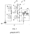
Referring now to Fig. 1, there is shown generally at 10, a schematic diagram for a known driver
circuit 12 for providing a sustaining voltage to a flat Plasma Display Panel (PDP) 14. The PDP
14 is represented in Fig. 1 by a plurality of capacitors 15 and a panel inductor 16 enclosed
within a dashed rectangle. The sustainer driver 12 for a TS PDP is required to make a 600-V
transition with a 200-ns rise time. This has traditionally been done using a series-resonant
network, split into two series-resonant sections, as shown in Fig. 3, with each series-resonant
section driving one end of the sustainer capacitance of the PDP 14. As shown in Fig. 1, each
series-resonant section is composed of an driver inductor 17 plus a series combination of a
MOSFET (IRF740) 18 and a pn diode (MUR1540) 20. The left portion of the driver section 12 is
connected through a driver capacitor 22 to ground while the right portion of the driver section 12
is connected between a power supply 24 and ground. A first driver diode 26 is connected
between the input to the PDP 14 and the power supply 24 while a second driver diode 28 is
connected between the input to the PDP 14 and ground.
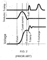
The operation of the driver circuit 10 is illustrated in Figs. 2 and 2A. The MOSFET's are
sequentially switched between conducting and non-conducting states by a logic circuit (not
shown). As the driver section 12 operates, charge flows through the driver inductance 17 and
back and forth between the PDP 14 and driver capacitance 22. The combined inductors and
capactiors of the driver section 12 and the PDP 14 form a resonant circuit. As shown in Fig. 2, a
resonant transition is then expected to be a half-wave pulse of current, driving the sustainer
capacitance of the PDP panel 14 through most of its voltage transition, which is then completed
by the loose turn-on of clamping MOSFET's (IRFP360), which are also expected to carry the
sustainer discharge current. The resonant loop on any given resonant transition therefore
includes two IRF740's, 18, two MUR1540's, 20, two resonant inductors 16 and 17, and the
sustainer capacitance 15, all in series. The bottom curve in Figs. 2 and 2A represents the
sustaining voltage applied to the PDP 14 while the middle curve represents the current flowing
through the driver inductor 17 and the upper curve represents the current supplied by the clamp
in the driver circuit. As shown in Fig. 2, the clamp occurs after the ramp up. This requires a fast
voltage ramp up time in order to complete the sequence in the allocated time. Because of the
fast voltage ramp up, ringing can occur, as also is apparent in Fig. 2. At time treturn, the driver
operates in a similar manner to return the sustainer voltage to the original voltage level.
It has been found that the driver section 12 shown in Fig. 1 recovers about 90% of the energy
normally lost in driving the panel capacitance 15. Accordingly, a PDP using the circuit shown in
Fig. 1 can operate with only about 10% of the power required by earlier prior art PDP's. Further
details of the sustainer driver circuit are included in U.S. Patent No. 5,081,400 that issued on
January 14, 1992. A complete sustainer driver circuit is shown in Fig. 3, where both driver
sections 12 and 26 are illustrated. Components shown in Fig. 3 that are similar to components
shown in Fig. 1 have the same numerical identifiers. The driver section 12 on the left in Fig. 2 is
operative to raise the sustaining voltage while the driver section 26 on the right in Fig. 3 is
operative to return the sustaining voltage to the original level.
Further details of the structure and operation of the above described sustaining voltage supplies
are set forth in U.S. Patent No. 4,866,349 that issued on September 12, 1989.
The prior art sustainer voltage driver circuits are complex and require a number of switching
FET's. Accordingly, it would be desirable to provide a simpler driver circuit that would include
less expensive components.
Summary of Invention
This invention relates to a method and apparatus for resonant injection of discharge energy into
a flat plasma display panel.
The present invention is directed toward a sustainer voltage driver circuit for a flat plasma
display panel that includes a driver inductor having at least a first end and a second end, the
second end of the inductor being adapted to be connected to an input port of the flat plasma
display panel. The driver circuit also includes a first electronic switch connected to the first end
of the driver inductor and a second electronic switch also connected to the first end of the driver
inductor. The circuit further includes at least one variable voltage supply connected across the
first and second electronic switches. A first driver capacitor is connected between the second
electronic switch and ground and a second driver capacitor is connected between the second
electronic switch and a voltage feedback point. A first driver diode is connected between the
second end of the driver inductor and the voltage feedback point and a second driver diode is
connected between the second end of the driver inductor and ground. The driver circuit also
includes a logic circuit connected to and operative to control the first and second electronic
switches and the variable voltage supply.
The logic circuit is also is connected to said feedback point and is responsive to the voltage
level at said voltage feedback point to adjust the output voltage level of said voltage supply.
Furthermore, the logic circuit is operative to set the variable voltage supply at an appropriate
level to inject sufficient energy during a transition of a sustaining voltage to a resonant condition
to establish a plasma discharge within the flat plasma display panel
In the preferred embodiment, the first and second electronic switches include a series
connection of an IGBT and a diode. Additionally, when connected to a plasma display panel the
driver circuit resonates with the panel such that the total power required to operate the panel is
reduced.
The present invention also contemplates a method of driving a flat plasma display panel that
includes the steps of providing a driver circuit that includes at least one adjustable voltage
supply. An energy requirement for the display panel is then determined and the voltage supply
levels are set to correspond to the desired energy requirement. The transition to the a resonant
condition for the sustaining voltage is begun and, if desired, sufficient energy is supplied to the
panel during the transition stage to establish a plasma discharge within the flat plasma display
panel.
The present invention also contemplates an alternate embodiment of the driver circuit for a flat
plasma display panel that includes a first switching device having a first end and a second end
with the first end adapted to be connected to a sustaining voltage supply. The driver circuit
further includes a transformer having a primary winding and a secondary winding. The
transformer primary winding having first and second ends with the first end connected to the
second end of the first switching device and the second end , said first end of said primary
winding being, said second end of said primary winding being adapted to be connected to a
sustaining voltage input port of the flat plasma display panel. Additionally, the driver circuit
includes a second switching device connected across the transformer secondary winding. The
first and second switching devices being selectively switched between conducting and non-conducting
states such that energy is stored in a field generated by the transformer windings for
injection into the plasma display panel.
The invention further contemplates that the injected energy is sufficient to both transition the
voltage across the flat plasma display panel to a desired sustainer voltage level and to provide
current to initiate the desired gas discharges within the flat plasma display panel
The present invention also contemplates a method for operating the alternate embodiment of
the driver circuit described immediately above. The method for operating includes the steps of
placing the first switching device in a conducting state while the second switching device is in a
non-conducting state to cause a voltage to begin to increase at a generally increasing rate upon
the display panel. The first switching device in then placed in a non-conducting state while the
second switching device is in a non-conducting state to cause the voltage upon the display
panel to continue to increase at a generally constant rate. Next, the first switching device is
returned to a conducting state while the second switching device is also placed in a conducting
state to cause the voltage upon the display panel to continue to increase at a slower rate and to
be clamped at predetermined voltage level while energy is stored within the B-field established
in the transformer coils by the flow of current within the transformer secondary coil. The first
switching device is then placed in a non-conducting state while the second switching device
remains in a conducting state to continue to store energy within the B-field established in the
transformer coils by the flow of current within the transformer secondary coil. Finally, the second
switching device is returned to a non-conducting state to inject the stored energy into the display
panel while maintaining the voltage applied to the flat plasma display panel at essentially a
clamped voltage level.
Various objects and advantages of this invention will become apparent to those skilled in the art
from the following detailed description of the preferred embodiment, when read in light of the
accompanying drawings.
Brief Description of Drawings
Fig. 1 is a schematic circuit diagram for a section for a prior art driver circuit for supplying a
sustaining voltage to a flat plasma display panel.
Fig. 2 illustrates voltage and current waveforms generated by the driver circuit shown in Fig. 1.
Fig. 2A illustrates a complete cycle of voltage and current waveforms generated by the driver
circuit shown in Fig. 1.
Fig. 3 is a schematic diagram for a complete driver circuit that includes the section shown in Fig.
1.
Fig. 4 is a schematic diagram for a section of a driver circuit for supplying a sustaining voltage to
a flat plasma display panel in accordance with the invention.
Fig. 5 illustrates voltage and current waveforms generated by the driver circuit shown in Fig. 4.
Fig. 5A is a flow chart for the operation of the driver circuit shown in Fig. 4.
Fig. 6 is a schematic diagram for an alternate embodiment of the driver circuit section shown in
Fig. 5.
Fig. 7 is a schematic diagram for a complete driver circuit that includes the circuit driver section
shown in Fig. 5.
Fig. 8 is a schematic diagram for a section of an alternate embodiment of the driver circuit
shown in Fig. 4.
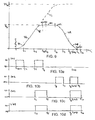
Fig. 9 illustrates voltage waveform generated by the driver circuit shown in Fig. 8.
Fig. 10 illustrates the switching sequence used by the switches in the circuit diagram shown in
Fig. 8 to generate the voltage waveform shown in Fig. 9.
Fig. 11 is an alternate embodiment of the circuit shown in Fig. 8.
Detailed Description
Referring again to the drawings, there is illustrated in Fig. 4 an improved circuit 30 for a section
of a PDP sustainer voltage driver. Components shown in Fig. 4 that are similar to components
shown in Fig. 1 have the same numerical identifiers. As shown in Fig. 4, the four MOSFET'S 18
of the prior art driver ciruit 12 have been replaced with first and second Injection Gate Bipolar
Transistors (IGBT's) 32 and 34 that are sequentially switched between conducting and non-conducting
states by a logic control circuit 39. In the preferred embodiment, IRG4BC40W
IGBT'S are used. The IGBT's 32 and 34 were identified as more promising than the MOSFET's
18 for use in the resonant drive circuit because their on-state voltage drops do not increase
proportionately with increasing conduction current. Because of the resonant circuit, the turn-off
times of the IGBT's 32 and 34 are not an issue. While the preferred embodiment of the invention
is illustrated as using IGBT's, it will be appreciated that the invention also can be practiced with
other conventional electronic switches, such as FET's, bipolar transistors or the like.
The first IGBT 32 has a cathode that is connected to the anode of a first MUR diode 36. In the
preferred embodiment, MUR 1540 diodes are used. The cathode of the first diode 36 is
connected to a first end of the driver inductor 17. The anode of the second IGBT 34 is
connected to the cathode of a second MUR diode 38. The anode of the second diode 38 is also
connected to the first end of the driver inductor 17.
The cathode of the second IGBT 34 is connected to the negative terminal of a series
combination of two variable voltage supplies 40 and 42 while the anode of the first IGBT 32 is
connected to the positive terminal of the combined voltage supplies 40 and 42. The variable
voltage supplies 40 and 42 are conventional programmable voltage supplies such as, for
example, flyback transformers, buck-up power supplies, flyback voltage sources or the like. The
voltage supplies 40 and 42 are connected to and controlled by the logic control 39. As will be
described below, the voltage supplied by the supplies 40 and 42 varies from about one quarter
of the sustainer voltage when no plasma discharges are present to an elevated level that is a
function of the amount of energy required to initiate a plasma discharge.
The series connected diodes 36 and 38 provide a turn-off function for the IGBT's 32 and 34. As
described above, the cathode of the first diode 36 and the anode of the second diode 38 are
connected to a first end of the driver inductor 17. The second end of the driver inductor 17 is
connected to the input port A of the PDP 14. While the driver inductor 17 is illustrated as having
two end connections, it will be appreciated that the invention also may be practiced with a driver
inductor having one or more taps between the first and second ends thereof (not shown). The
intermediate taps on such an inductor would allow connection of conventional circuits to boost
the voltage applied to the PDP input port A.
The connection between the two variable voltage supplies 40 and 42 is connected to a common
node between first and second driver capacitors 22 and 44. The first driver capacitor 22 is also
connected to ground while the second driver capacitor is connected to the voltage feedback
point 24. Similar to the prior art driver circuit 12 described above, the driver circuit 30 also
includes a first driver diode 26 that is connected between the input port A of the PDP 14 and the
voltage feedback point 24 while a second driver diode 28 is connected between the input port A
and ground.
The operation of the improved driver circuit 30 will now be described. Typical waveforms
generated by the operation of the circuit 30 are shown in Fig. 5. The operation is also illustrated
by the flow chart in Fig. 5A. The present invention contemplates two modes of operation of the
PDP 14. In a first mode, which is illustrated by the broken lines in Fig. 5, there is no plasma
discharge. In the second mode, which is illustrated by the solid lines in Fig. 5, there is a plasma
discharge.
In decision block 50 in Fig. 5A, it is determined which mode of operation is desired. Assuming
the first mode, the method proceeds to functional block 52 where the voltage levels for the
variable voltage supplies 40 and 42 are set at approximately one quarter of the sustaining
voltage level. Ideally, the voltages would be at one quarter of the sustaining voltage level;
however, due to the need to compensate for component losses, the voltage levels are actually
set slightly above the one quarter voltage level. At this point, the voltage at the PDP input port A
is at ground or zero potential. At tstart the first electronic switch 32 is changed from a non-conducting
state to a conducting state, as shown in functinal block 54. The series resonance of
the driver inductor 17 and the parallel capacitors 15 of the PDP 14 establish a resonant rise in
voltage at the input port A. The time constant for the voltage rise is determined by the total
inductance of the driver inductor 17 and the panel inductor 16 and the capacitance of the panel
capacitors 15. The current through the driver inductance 17 reaches a peak at tpeak current after
which the current begins to decrease as the voltage continues to rise. The voltage reaches a
peak at tresonance. As shown in Fig. 5A, because the first mode is in effect, the operation
continues through decision block 56 to functional block 58 where the first electronic switch 32 is
returned to its non-conducting state at toff with the voltage at the sustaining voltage level. Once
the intended sustaining voltage is reached, it is held by the operation of the driver diode 26 and
the PDP capacitors 15.
After a predetermined time has elapsed, the second electronic switch 34 is changed to a
conduction state (not shown) The second electronic switch co-operates with the driver inductor
17 and the PDP panel capacitance in a similar manner as described above to drive the
sustaining voltage back to its original value (not shown).
The second mode of operation includes establishment of a plasma discharge. Accordingly, the
operation transfers from the decision block 50 to 60 where the logic control 39 determines the
energy requirement to establish the desired plasma discharge. Then the voltage levels are set
in functional block 52 at a higher level to cause an injection of additional energy during the
transition to resonance of the PDP 17. As shown by the lower solid curve in Fig. 5, the voltage
increases at a faster rate since the voltage supplies 40 and 42 are set for higher outputs.
Because of the increased energy, a plasma discharge is established at tdischarge, as illustrated in
Fig. 5. After the discharge is established, the sustaining voltages are maintained as described
above. However, if the voltage supply voltages were set too high, the driver conductor will
conduct slightly and charge driver capacitor 44. The voltage appearing across the capacitor 44
is fedback from point 24 to the logic control 39 which then adjusts the voltage levels in a
downward direction for the next cycle. Thus, the setting of the voltage outputs for the voltage
supplies 40 and 42 is dynamic. Also, the present invention injects energy during the transition to
resonance for the PDP sustaining voltage. Because the injection of energy occurs during the
transition, the transition can last longer, thereby reducing the amount of total energy required to
operate the PDP17. Also, as described above, a single driver circuit 30 is capable of driving the
PDP with two sustaining voltage levels.
During simulations, the inventor has determined that the improved circuit increased the peak
ringing current from 27 amps needed for the same PDP with the prior art driver circuit 12 to 32
amps while reducing the power consumption from 42 watts to 27 watts. Additionally, the
operationg temperature of the switching devices was reduced from about 120°C to about 90°C.
Also significant is the smoothing of the voltage applied to the PDP 14, as illustrated in the
bottom graph. The ringing in the voltage associated with the clamping action as shown in Fig. 2
for the prior art driver circuit has been eliminated.
The preceding results were obtained with the bridge timing set so that the resonant transition
was well completed before activation of the clamps. Setting the clamping time close to the
completion of the resonant transition can increase the sustainer losses by about 35%. The
inventor found that the temperature of the MUR1540 diode junctions during reverse-recovery
can adversely effect their turn-off time and thereby lower the efficiency.
After making these measurements, the inventor also investigated improvements to the gate
drive voltage for the resonant switches 32 and 34. The measured value was between 12 and 9V
initially and the inventor believes that an increase will give a second-order improvement in
circuit efficiency.
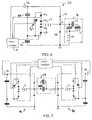
An alternate embodiment of the improved driver circuit is illustrated at 70 in Fig. 6. Components
shown in Fig. 6 that are similar to components shown in Fig. 4 have the same numerical
designators. In the alternate embodiment, the two variable voltage supplies 40 and 42 have
been replaced with a single variable voltage supply 72. The positive terminal of the supply 72 is
connected to the anode of the first IGBT 32 while the negative terminal of the supply 52 is
connected to the cathode of the second IGBT 34. Thus, the alternate embodiment of the circuit
70 uses less components than the embodiment illustrated in Fig. 4. The operation of the
alternate embodiment 70 is the same as described above; however, the circuit 70 is equivalent
to one section of the prior art circuit shown in Fig. 3. Thus the driver circuit 70 is only capable to
increase the sustainer voltage. A second driver circuit 80, which is shown in Fig. 7 is needed to
return the sustainer voltage to the original level.
The invention further contemplates replacement of the MUR1540 series diodes 36 and 38 with
faster diodes. It is believed that faster diodes will improve the resonant transition, while
decreasing both losses in the clamping bridge as well as switching losses in the circuit.
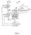
The invention also contemplates another alternate embodiment 82 of the driver section circuits,
as illustrated by the schematic circuit diagram shown in Fig. 8. As before, components in Fig. 8
that are similar to components shown in earlier figures have the same numerical identifiers. As
shown in Fig. 8, the alternate embodiment 82 includes a first pair of electronic switches, SW1
and SW2, that are connected in series between voltage supplies VS1 and VS2. While FET's are
shown for the electronic switches, SW1 and SW2, it will be appreciated that the use of FET's is
exemplary and that other the invention also can be practiced with other switching devices. The
diodes, D1 and D2 shown with dashed lines represent the internal characteristics of the FET's.
The gates of the FET's are connected to a logic control 84 that is operational to switch the
FET's between their conducting and non-conducting states. The voltage supplies VS+ and VS-
have fixed output voltages set at the ± the sustaining voltage value for the PDP 14 that is driven
by the circuit 82. While the sustaining voltages are shown as being plus/minus, it will be
appreciated that voltages are measured from a reference voltage value that can be selected as
non-zero.
The common connection point 86 between the electronic switches, SW1 and SW2, is connected
through a transformer 88 to a first input port 90 of the PDP 14. In the preferred embodiment, the
transformer 88 is an air core transformer having a primary winding L1 and secondary winding
L2. The transformer windings are wound to match the equivalent capacitance of the PDP 14
and the desired PDP response time. Generally, the inductance of the transformer 88 is low to
meet these criteria. The invention can be practiced with a transformer turns ratio of 1:1;
however, selecting turns ratio that steps down the voltage in the secondary circuit allows use of
lower voltage rating devices in the transformer secondary circuit. Accordingly, in the preferred
embodiment, a step down voltage turns ration of 4:1 or 5:1 is used.
The secondary circuit of the transformer 88 is connected to a second pair of electronic switches
SW3 and SW4, that are connected in series with one another. While FET's are again shown for
the electronic switches, SW3 and SW4, it will be appreciated that the use of FET's is exemplary
and that other the invention also can be practiced with other switching devices. The diodes, D3
and D4 shown with dashed lines represent the internal characteristics of the FET's. The gates of
the FET's are connected to the logic control 84 that is operational to switch the FET's between
their conducting and non-conducting states. While two lines are shown connecting the FET
gates to the logic control 88, both FET,s, SW3 and SW4, are operated together and a single line
(not shown) can be used to connect the logic control 84 to both FET gates. When the turns ratio
for the transformer 88 is selected to step down the secondary voltage from the primary, lower
voltage rated devices can be utilized for the second pair of electronic switches SW3 and SW4
than for the first pair of electronic switches SW1 and SW2, allowing a reduction in cost.
The operation of the driver circuit 82 will now be explained with reference to Figs. 9 and 10. Fig.
9 illustrates the sustaining voltage waveform generated by the circuit 82 and applied the first
input port 90 of the PDP 14. The time sequencing for switching the electronic switches SW1,
SW2, SW3 and SW4 in the driver circuit 82 is illustrated in Fig. 10 with the portion of the figure
labeled 10a corresponding to the operation of electronic switch SW1 between its conducting
and non-conducting states, which are indicated by the legends "on" and "off", respectively.
Initially, all four switches SW1, SW2, SW3 and SW4 are in their non-conducting state. At time
tstart the logic control 84 is operative to cause the upper switch SW1 of the first pair of electronic
switches to change to its conducting state and thereby apply the voltage VS+ to the first input
port 90 of the PDP 14. Because of the inherent capacitance of the PDP 14, the voltage beings
applied to the PDP input port 90 begins increase, as shown by the portion of the curve labeled
92 in Fig. 9, as the series resonance of the transformer primary coil L1 and the parallel
capacitors of the PDP 14 establish a resonant rise in voltage at the input port 90 of the PDP 14.
The total energy injected into the resonant circuit is sufficient to both transition the voltage
across the PDP 14, which appears as a capacitance to the driver circuit 82, to the desired
sustainer voltage level; and to provide sufficient current to establish the required gas discharges
within the PDP 14. When time reaches t2, the logic control 84 is further operative to cause the
upper switch SW1 of the first pair of electronic switches to change to its non-conducting state.
However, the voltage at the PDP input port 92 continues to ncrease as shown by the portion of
the curve labeled 94 in Fig. 9 and, if nothing further would happen would follow the dashed line
labeled 96, to a value of approximately 2VS+.
To control the voltage applied to the PDP 14, the logic control 84 again causes the upper switch
SW1 of the first pair of electronic switches to change to its conducting state at t3 while also
causing the second pair of electronic switches SW3 and SW4 in the transformer secondary
circuit to change to their conducting state. With the FET's shown in the secondary circuit in Fig.
8, only one FET actually conducts while the internal diode of the other FET allows the
secondary current to flow. However, the configuration of the second pair of FET's allows the
secondary current to flow in either direction as the needed by the voltage being applied to the
PDP 14. As the secondary current flows, energy is stored in the B-field generated by the
transformer 88. As a result, the increasing voltage applied to the PDP input port 90 is clamped
to a steady value of about VS+, as shown by the portion of the curve labeled 98 in Fig. 9.
At t4, the logic control 84 causes the upper switch SW1 of the first pair of electronic switches to
change back to its non-conducting state, as shown in Fig. 10a, while the second pair of
electronic switches SW3 and SW4 in the transformer secondary circuit remain in their
conducting state until time t5, as shown in Figs. 10c and 10d. There is sufficient energy stored in
the B-field with the secondary current that energy is prevented from being discharged within the
PDP 14 between the times t4 and t5. The duration of the time period between the times t4 and t5
is labeled ΔT and is selected to provide appropriate conditions and voltage phase relationships
for the PDP 4.
The voltage applied to the PDP input port 90 can be further controlled by adding an optional
capacitor 94 in the transformer secondary circuit and across the second pair of electronic
switches SW3 and SW4, as illustrated with dashed lines in Fig. 8. The optional capacitor 94
forms a resonant circuit with transformer secondary inductance L2. Between t5 and t6, all of the
electronic switches SW1, SW2, SW3 and SW4 are again in their non-conducting state and the
voltage at the PDP input port 90 remains at approximately VS+, as shown by the portion of the
curve in Fig. 9 labeled 100.
Beginning at t6, the voltage at the PDP input port 90 is returned to the initial voltage level by
further operation of the electronic switches. At t6, the logic control 84 is operative to cause the
lower switch SW2 of the first pair of electronic switches to change to its conducting state and
thereby apply the voltage VS- to the first input port 90 of the PDP 14. Because of the inherent
capacitance of the PDP 14, the voltage begins applied to the PDP input port 90 begins
decrease, as shown by the portion of the curve labeled 102 in Fig. 9. When time reaches t7, the
logic control 84 is further operative to cause the lower switch SW1 of the first pair of electronic
switches to change to its non-conducting state. However, the voltage at the PDP input port 92
continues decrease as shown by the portion of the curve labeled 104 in Fig. 9 and, if nothing
further would happen would continue to decrease to a value of approximately 2VS-.
To continue to control the voltage applied to the PDP 14, the logic control 84 again causes the
lower switch SW2 of the first pair of electronic switches to change to its conducting state at t8
while also causing the second pair of electronic switches SW3 and SW4 in the transformer
secondary circuit to change to their conducting state. With the voltage decreasing, the
secondary current now flows in the opposite direction from the flow during the increasing
voltage portion of the PDP driver circuit operation described above. However, as described
above, the configuration of the second pair of FET's allows the secondary current to flow in
either direction as the needed by the voltage being applied to the PDP 14. As the secondary
current flows, energy is again stored in the B-field generated by the transformer 88. As a result,
the decreasing voltage applied to the PDP input port 90 is clamped to a steady value of about
the initial voltage, as shown by the portion of the curve labeled 108 in Fig. 9.
At t9, the logic control 84 causes the lower switch SW2 of the first pair of electronic switches to
change back to its non-conducting state, as shown in Fig. 10a, while the second pair of
electronic switches SW3 and SW4 in the transformer secondary circuit remain in their
conducting state until time t10, as shown in Figs. 10c and 10d. There is sufficient energy stored
in the B-field with the secondary current that energy is prevented from being discharged with in
the PDP 14 between the times t9 and t10. The duration of the time period between the times t9
and t10 is labeled ΔT' and is selected to provide appropriate conditions and voltage phase
relationships for the PDP 4. The invention contemplates that the duration ΔT' may or may not be
equal to ΔT.
The invention further contemplates that the energy remaining in the PDP 14 is monitored during
the driver circuit cycle described above. A feedback circuit (not shown) would determine the
magnitude of any residual energy remaining in the PDP 14 when the input port voltage is
returned to its initial value and the sustaining voltage adjusted during the next cycle to
compensate for the remaining energy by supplying less energy to the PDP 14. The
compensation can take several forms. For example the time periods during which the sustaining
voltage is applied to the PDP 14 can be reduced. Alternately, a PWM voltage can be used for
the sustaining voltage, in which case the duty cycle of the PWM waveform can be modified to
reduce, or increase, the energy supplied to the PDP 14. Additionally, a combination of changing
the time period and PWM modulation can be utilized.
Additionally, as described above, the total energy injected into the resonant circuit is sufficient to
both transition the voltage across the PDP 14, which appears as a capacitance to the driver
circuit 82, to the desired sustainer voltage level; and to provide sufficient current to establish the
required gas discharges within the PDP 14. Accordingly, the logic control 84 also is connected
to the PDP control circuit (not shown). The logic control 84 receives information from the PDP
control circuit concerning the percentage of the PDP 14 that is to be illuminated by gas
discharges. Since the current required for establishing the gas discharges is proportional to the
amount of the PDP to be illuminated, the logic control 84 is operable to convert the percentage
to a current demand and then adjust the waveform PWM and/or on times to assure that
sufficient energy is injected into the PDP 14 to provide both the desired sustainer voltage level
and the current needed to establish the desired gas discharges.
Similar to the driver circuits shown above, the PDP 14 in Fig. 8 has a second input port 110 that
is connected to a second driver circuit (not shown) that is a mirror image of the driver circuit 82
described above. The second driver circuit is operative to provide a sustaining voltage to the
PDP 14 that is the inverse of the voltage waveform shown in Fig. 9.
Another alternate embodiment of the driver circuit is shown generally at 120 in Fig. 11. As
before, components in Fig. 11 that are similar to components shown in the preceding figures
have the same numerical designators. The driver circuit 120 includes a second air core
transformer 122 having a primary coil that is connected between the PDP input port 90 and the
first driver circuit 82. The driver circuit 120 also has a third air core transformer 124 having a
primary coil that is connected between the PDP output port 110 and the second driver circuit
(not shown). One end of each of the secondary coils of the second and third transformers 122
and 124 are connected together while the other ends of the secondary coils are connected to
ground. The additional transformers allow balancing of the voltages applied to the two PDP
ports 90 and 110 by transferring energy across the PDP 14 by means of the current flowing
between the transformer secondaries.
The principle and mode of operation of this invention have been explained and illustrated in its
preferred embodiment. However, it must be understood that this invention may be practiced
otherwise than as specifically explained and illustrated without departing from its spirit or scope.