EP1324209A1 - Multiprocessor system, data processing system, data processing method, and computer program - Google Patents
Multiprocessor system, data processing system, data processing method, and computer program Download PDFInfo
- Publication number
- EP1324209A1 EP1324209A1 EP01972530A EP01972530A EP1324209A1 EP 1324209 A1 EP1324209 A1 EP 1324209A1 EP 01972530 A EP01972530 A EP 01972530A EP 01972530 A EP01972530 A EP 01972530A EP 1324209 A1 EP1324209 A1 EP 1324209A1
- Authority
- EP
- European Patent Office
- Prior art keywords
- data
- data processing
- processors
- processing
- broadcast
- Prior art date
- Legal status (The legal status is an assumption and is not a legal conclusion. Google has not performed a legal analysis and makes no representation as to the accuracy of the status listed.)
- Granted
Links
Images



Classifications
-
- G—PHYSICS
- G06—COMPUTING OR CALCULATING; COUNTING
- G06F—ELECTRIC DIGITAL DATA PROCESSING
- G06F15/00—Digital computers in general; Data processing equipment in general
- G06F15/16—Combinations of two or more digital computers each having at least an arithmetic unit, a program unit and a register, e.g. for a simultaneous processing of several programs
-
- G—PHYSICS
- G06—COMPUTING OR CALCULATING; COUNTING
- G06F—ELECTRIC DIGITAL DATA PROCESSING
- G06F15/00—Digital computers in general; Data processing equipment in general
- G06F15/76—Architectures of general purpose stored program computers
- G06F15/80—Architectures of general purpose stored program computers comprising an array of processing units with common control, e.g. single instruction multiple data processors
- G06F15/8007—Architectures of general purpose stored program computers comprising an array of processing units with common control, e.g. single instruction multiple data processors single instruction multiple data [SIMD] multiprocessors
-
- G—PHYSICS
- G06—COMPUTING OR CALCULATING; COUNTING
- G06T—IMAGE DATA PROCESSING OR GENERATION, IN GENERAL
- G06T1/00—General purpose image data processing
- G06T1/20—Processor architectures; Processor configuration, e.g. pipelining
Definitions
- the multi-processor system is configured with the addition of a sort mechanism that obtains the identification data from the processor that has finished data processing among the plurality of processors and sends the obtained identification data to the controller in a predetermined order.
- the controller is configured to obtain the results of processing based on the identification data received from the sort mechanism.
- the sort mechanism is configured to determine an order of sending the identification data, based on the priority data.
- the sort mechanism allows the controller to obtain the results of processing in a necessary order and efficiently execute complicated processing in the whole system.
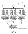
- the BCMC 10 is connected to all cell processors 20 via a broadcast channel (a communication channel through which information can be disseminated to several recipients simultaneously).
- a broadcast channel a communication channel through which information can be disseminated to several recipients simultaneously.
- the WTA/sum circuits 30 are connected as illustrated in FIG. 1. More specifically, the WTA/sum circuits 30 are connected to have a pyramidal shape with the side of the cell processors 20 located at the first stage. The input terminals of each WTA/sum circuit 30 at the first stage are connected to two cell processors 20 while the output terminal thereof is connected to an input terminal of a WTA/sum circuits 30 at the second stage.
- the present invention can be carried out by cascading the WTA/sum circuits 30.
- the input terminals of each WTA/sum circuit 30 at the first stage are connected to two cell processors 20 while the output terminal thereof is connected to an input terminal at the next upper stage.
- the input terminals of each WTA/sum circuit 30 at the second stage and later are connected to an output terminal of a WTA/sum circuit 30 at the next lower stage and a cell processor while the output terminal thereof is connected to an input terminal at the next upper stage.
- the WTA/sum circuit 30 at the uppermost stage the input terminals thereof are connected to an output terminal of a WTA circuit 30 at the lower stage and a cell processor 20 while the output terminal thereof is connected to the BCMC 10.
- the BCMC 10 includes a CPU core 101 that controls the entire operations of the multi-processor system 1, a re-writable main memory 102 such as an SRAM (Static Random Access Memory), and a DMAC (Direct Memory Access Controller) 103, all of which are connected to one another by a bus B1.
- the CPU core 101 is a semiconductor device to be mounted on a computer, which reads and executes a predetermined program in cooperation with the main memory 102 to provide a function for performing the characteristic data processing of the present invention.
- the main memory 102 is used as a shared memory for the entire system.
- the CPU core 101 loads a boot program from the external memory on startup, and executes the boot program to invoke an operating system. It also reads various kinds of data necessary for data processing from the external memory and expands them to the main memory 102. Data such as state variable values of the cell processors 20 are to be stored in the main memory 102. The state variable value is placed into the main memory at the address corresponding to the cell address of the cell processor 20 that has calculated its own state variable value.
- Each cell processor 20 performs data processing after sorting out necessary data from the broadcast data, and informs, at the time of completion of the data processing, the WTA/sum circuit 30 of the completion.
- Each cell processor 20 sends the state variable value which is the result of data processing to the BCMC 10 in response to an instruction from the BCMC 10.
- the cell processors 20 are connected to each other in a ring topology via a shared memory (not shown).
- the cell processors 20 may synchronously perform their data processing. Alternatively, the cell processors 20 may asynchronously perform their data processing.
- FIG. 3 shows a configuration example of the cell processor 20.
- the cell CPU 201 is a processor that has a programmable floating-point calculator and controls operations of the local cell processor 20 to perform data processing.
- the cell CPU 201 obtains the broadcast data subjected to broadcasting from the BCMC 10 via the input buffer 202. Then, the cell CPU 201 determines, based on the cell address of the paired data, whether the obtained broadcast data are those necessary for the processing that the cell CPU 201 should perform.
- the cell CPU 201 writes the state variable value to the corresponding address of the data memory 207, if necessary.
- the cell CPU 201 reads the state variable value from the data memory 207 and performs data processing. Then, the cell CPU 201 writes a result of data processing to the output buffer 203, and sends data, which indicate completion of the data processing, to the WTA/sum circuit 30.
- the input buffer 202 is for holding the broadcast data subjected to broadcasting from the BCMC 10.
- the broadcast data held are sent to the cell CPU 201 in response to a request from the cell CPU 201.
- the output buffer 203 is for holding the state variable value of the cell CPU 201.
- the state variable value held is sent to the BCMC 10 in response to a request from the BCMC 10.
- the input buffer 202 and the output buffer 203 may transmit and receive data for control.
- the WTA buffer 204 receives data which indicate completion of the data processing from the cell CPU 201 at the completion of the data processing performed by the cell CPU 201. Then, the WTA buffer 204 transmits the received data to the WTA/sum circuit 30 to inform the WTA/sum circuit 30 of the completion of the data processing.
- the data indicative of the completion of the data processing include, for example, the ID of the local cell processor 20 and priority data that are used to determine the priority. The priority data are necessary when the state variable value in the output buffer 203 is read out to the BCMC 10.
- the program controller 205 is for fetching from the BCMC 10 a program that defines the operation of the cell processor 20.
- the program that defines the operation of the cell processor 20 includes a program for data processing that is carried out by the cell processor 20 and a data selection program for determining data necessary for processing that is carried out by that cell processor 20.
- the program also includes a priority determination program for determining the priority which is necessary when a result of processing is read out to the BCMC 10.
- the instruction memory 206 is for storing the program(s) fetched by the program controller 205.
- the stored program is read to the cell CPU 201 as required.
- the data memory 207 is for storing data to be processed by the cell processor 20.
- the broadcast data determined to be necessary by the cell CPU 201 are written thereto.
- the broadcast data are stored in the data memory 207 at the address corresponding to the cell address.
- a part of the data memory 207 is connected to a cell processor 20 that is adjacent thereto via the shared memory. This makes it possible to transmit and receive data to and from the adjacent cell processor 20 for each cycle.
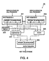
- Each of the first input register 301 and the second input register 302 has an integer register and a floating-point register.
- the ID is written to the integer register for example, and the priority data are written to the floating-point register.
- the selector switch 303 activates either the comparator 304 or the adder 305. More specifically, the selector switch 303 enables only one of them in accordance with an operation mode.
- the operation mode is determined by an instruction from, for example, the BCMC 10. The operation mode will be described later.
- the comparator 304 compares the floating-point values which are held by the floating-point registers of the first input register 301 and the second input register 302. The comparator 304 writes the larger (or smaller) value and its associated integer to the output register 306.
- the adder 305 calculates the sum of the floating-point values which are held by the floating-point registers of the first input register 301 and the second input register 302, and writes the result of calculation to the output register 306.
- the WTA/sum circuit 30 has three operation modes as set forth below.
- the comparator 304 is activated by the selector switch 303.
- the comparator 304 compares the floating-point values A and B which are held by the floating-point registers of the first input register 301 and the second input register 302.
- the comparator 304 writes the larger (or smaller) value and its associated integer to the output register 306.
- the first input register 301 and the second input register 302 are cleared.
- the content of the output register 306 is written to the input register of the WTA/sum circuit 30 at the next upper stage. At this time, if the input register as a writing destination is not cleared, the writing is stalled and no writing is performed at this cycle. For this reason, the content of the output register 306 is to be written at the next cycle.
- the data the BCMC 10 receives from the WTA/sum circuit 30 at the uppermost stage are sorted in the increasing or decreasing order of the floating-point values.
- WTA/sum circuit 30 comprises input registers of the same number as the cell processors 20 in addition to a selector switch, a comparator, an adder, and an output register.
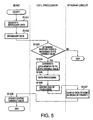
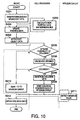
- FIG. 5 is a flowchart illustrating a flow of processing that is executed by this multi-processor system 1.
- the BCMC 10 produces broadcast data using a pair of data including a state variable value of a given cell processor 20 and a cell address of that cell processor 20 (step S101). Then, the BCMC 10 broadcasts the produced broadcast data to all cell processors 20 (step S102).
- each cell processor 20 When the broadcasting is completed, each cell processor 20 carries out data processing of the state variable value recorded on the data memory 207 to produce a new state variable value by using the data processing program stored in the instruction memory 206. The new state variable value is written to the data memory 207, and is also written to the output buffer 203 (step S105). Then, each cell processor 20 overwrites the address on the data memory 207 corresponding to its cell address, with the new state variable value.
- the WTA/sum circuit 30 at the first stage holds an ID in the integer register of the input register and the priority data in the floating-point register. In this event, the WTA/sum circuit 30 operates in the approximate sort mode. To this end, the selector switch 303 activates the comparator 304.
- the integer registers of the first input register 301 and the second input register 302 of the WTA/sum circuit 30 hold IDs sent from different cell processors 20. Each of the floating-point registers holds the priority data associated with the ID.
- the comparator 304 reads the priority data from the floating-point registers of the first input register 301 and the second input register 302, and compares them. As a result of the comparison, the comparator 304 writes the data of the higher priority and their corresponding IDs to the floating-point register and the integer register, respectively, of the output register 306.
- the input registers whose contents are written to the output register 306 are cleared.
- the IDs and the priority data written to the output register 306 are written to the input registers of the WTA/sum circuit 30 at the next upper stage.
- the BCMC 10 obtains a state variable value that has already been subjected to data processing, from the output buffer 203 of the cell processor 20 corresponding to the ID sent from the WTA/sum circuit 30.
- the address corresponding to the cell address that indicates the cell processor 20 that has performed the processing is overwritten with the obtained state variable value (step S108).
- Each cell processor 20 sorts out necessary data from the broadcast data instead of directly fetching the data that it requires from the main memory 102.
- the cell processor 20 performs processing while holding the data locally, so that high-speed processing can be made without any conflict of data.
- a first embodiment of the above-mentioned multi-processor system 1 is described specifically.
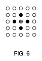
- the cell processor 20 stores a necessary group of lattice point data of the broadcast data in the data memory 207. Then, it reads the lattice point data sequentially out of the data memory 207 and performs data processing.
- Grouping the broadcast data makes it possible to process the data in a row or column direction, and data transfer via the shared data allows data processing in a row or column direction.
- processing for specifying the cell processor 20 that holds such data that are most similar to a feature of the input data is carried out as follows:
- the BCMC 10 broadcasts the input data to all cell processors 20.
- Each cell processor 20 calculates a differential value between a feature of the template data that it holds and a feature of the input data.
- the differential value is sent to the WTA/sum circuit 30 along with the ID.
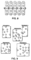
- n objects there are some variations in the spatial distribution of n objects and that the objects are divided into m clusters. For example, it is determined herein which one of (n-1) objects collides with a given object most strongly.
- FIG. 9 is a view illustrating objects in such a space, in which objects represented by a white circle are enclosed within a rectangle to form one cluster.
- the objects are divided into five clusters.
- the data indicative of the objects are broadcasted from the BCMC 10, and fetched to the cell processors 20 on a cluster-by-cluster basis.
- the cell processor 20 performs processing about a position and movement in the space in connection with the objects included in one fetched cluster.
Landscapes
- Engineering & Computer Science (AREA)
- Theoretical Computer Science (AREA)
- Computer Hardware Design (AREA)
- Physics & Mathematics (AREA)
- General Physics & Mathematics (AREA)
- General Engineering & Computer Science (AREA)
- Computing Systems (AREA)
- Software Systems (AREA)
- Multi Processors (AREA)
- Image Processing (AREA)
- Hardware Redundancy (AREA)
Abstract
Description
Claims (18)
said controller is adapted to generate and broadcast the broadcast data, the broadcast data including the identification data of the sending processors in addition to said results of the processing, and
said plurality of processors sort out the result(s) of processing necessary for the data processing that they perform at the subsequent timing, based on said identification data included in the received broadcast data.
said controller is configured to obtain said results of processing based on the identification data received from said sort mechanism.
the processor that has finished data processing sends, to said sort mechanism, said priority data about the processing along with its own identification data, and
said sort mechanism is configured to determine an order of sending said identification data, based on said priority data.
means for recording said priority data and said identification data that have sent from the sending processors, in said registers associated with the sending processors, and
a comparator for comparing said priority data to determine the order of the identification data recorded in the respective registers,
said sort mechanism being configured to determine an order of sending said identification data, based on the result of comparison obtained by said comparator.
data generating means that reads said processing result(s) stored in said memory and generates said broadcast data, the broadcast data including said processing result(s) and the received identification data.
means for sending to said controller the result of the data processing said data processing mechanism has done along with its own identification data in response to a request from said controller, and
means for sending process end notifying data to said sort mechanism in response to the completion of the data processing, the process end notifying data including its own identification data.
Applications Claiming Priority (5)
| Application Number | Priority Date | Filing Date | Title |
|---|---|---|---|
| JP2000294732 | 2000-09-27 | ||
| JP2000294732 | 2000-09-27 | ||
| JP2001289588A JP3426223B2 (en) | 2000-09-27 | 2001-09-21 | Multiprocessor system, data processing system, data processing method, and computer program |
| JP2001289588 | 2001-09-21 | ||
| PCT/JP2001/008434 WO2002027513A1 (en) | 2000-09-27 | 2001-09-27 | Multiprocessor system, data processing system, data processing method, and computer program |
Publications (3)
| Publication Number | Publication Date |
|---|---|
| EP1324209A1 true EP1324209A1 (en) | 2003-07-02 |
| EP1324209A4 EP1324209A4 (en) | 2008-12-17 |
| EP1324209B1 EP1324209B1 (en) | 2011-03-02 |
Family
ID=26600866
Family Applications (1)
| Application Number | Title | Priority Date | Filing Date |
|---|---|---|---|
| EP01972530A Expired - Lifetime EP1324209B1 (en) | 2000-09-27 | 2001-09-27 | Multiprocessor system, data processing system, data processing method, and computer program |
Country Status (10)
| Country | Link |
|---|---|
| US (1) | US7017158B2 (en) |
| EP (1) | EP1324209B1 (en) |
| JP (1) | JP3426223B2 (en) |
| KR (1) | KR100866730B1 (en) |
| CN (1) | CN1258154C (en) |
| AT (1) | ATE500556T1 (en) |
| AU (1) | AU2001292269A1 (en) |
| DE (1) | DE60144155D1 (en) |
| TW (1) | TWI229265B (en) |
| WO (1) | WO2002027513A1 (en) |
Families Citing this family (33)
| Publication number | Priority date | Publication date | Assignee | Title |
|---|---|---|---|---|
| US6989843B2 (en) * | 2000-06-29 | 2006-01-24 | Sun Microsystems, Inc. | Graphics system with an improved filtering adder tree |
| US8478811B2 (en) | 2002-10-08 | 2013-07-02 | Netlogic Microsystems, Inc. | Advanced processor with credit based scheme for optimal packet flow in a multi-processor system on a chip |
| US7346757B2 (en) * | 2002-10-08 | 2008-03-18 | Rmi Corporation | Advanced processor translation lookaside buffer management in a multithreaded system |
| US8176298B2 (en) | 2002-10-08 | 2012-05-08 | Netlogic Microsystems, Inc. | Multi-core multi-threaded processing systems with instruction reordering in an in-order pipeline |
| US7334086B2 (en) * | 2002-10-08 | 2008-02-19 | Rmi Corporation | Advanced processor with system on a chip interconnect technology |
| US9088474B2 (en) | 2002-10-08 | 2015-07-21 | Broadcom Corporation | Advanced processor with interfacing messaging network to a CPU |
| US8037224B2 (en) | 2002-10-08 | 2011-10-11 | Netlogic Microsystems, Inc. | Delegating network processor operations to star topology serial bus interfaces |
| US8015567B2 (en) | 2002-10-08 | 2011-09-06 | Netlogic Microsystems, Inc. | Advanced processor with mechanism for packet distribution at high line rate |
| US20050120185A1 (en) * | 2003-12-01 | 2005-06-02 | Sony Computer Entertainment Inc. | Methods and apparatus for efficient multi-tasking |
| JP4794194B2 (en) * | 2005-04-01 | 2011-10-19 | 株式会社日立製作所 | Storage system and storage control method |
| JP4555145B2 (en) | 2005-04-28 | 2010-09-29 | 富士通株式会社 | Batch scheduling program, batch scheduling method, and batch scheduling apparatus |
| US7444525B2 (en) * | 2005-05-25 | 2008-10-28 | Sony Computer Entertainment Inc. | Methods and apparatus for reducing leakage current in a disabled SOI circuit |
| US7970956B2 (en) * | 2006-03-27 | 2011-06-28 | Ati Technologies, Inc. | Graphics-processing system and method of broadcasting write requests to multiple graphics devices |
| US9596324B2 (en) | 2008-02-08 | 2017-03-14 | Broadcom Corporation | System and method for parsing and allocating a plurality of packets to processor core threads |
| JP5039950B2 (en) | 2008-03-21 | 2012-10-03 | インターナショナル・ビジネス・マシーンズ・コーポレーション | Object movement control system, object movement control method, server, and computer program |
| US7870365B1 (en) | 2008-07-07 | 2011-01-11 | Ovics | Matrix of processors with data stream instruction execution pipeline coupled to data switch linking to neighbor units by non-contentious command channel / data channel |
| US8131975B1 (en) | 2008-07-07 | 2012-03-06 | Ovics | Matrix processor initialization systems and methods |
| US7958341B1 (en) | 2008-07-07 | 2011-06-07 | Ovics | Processing stream instruction in IC of mesh connected matrix of processors containing pipeline coupled switch transferring messages over consecutive cycles from one link to another link or memory |
| US8145880B1 (en) | 2008-07-07 | 2012-03-27 | Ovics | Matrix processor data switch routing systems and methods |
| US8327114B1 (en) | 2008-07-07 | 2012-12-04 | Ovics | Matrix processor proxy systems and methods |
| CN101478785B (en) * | 2009-01-21 | 2010-08-04 | 华为技术有限公司 | Resource pool management system and signal processing method |
| JP4539889B2 (en) * | 2009-02-18 | 2010-09-08 | 日本電気株式会社 | Processor and data collection method |
| KR101651871B1 (en) * | 2009-12-28 | 2016-09-09 | 삼성전자주식회사 | Job Allocation Method on Multi-core System and Apparatus thereof |
| US8850262B2 (en) * | 2010-10-12 | 2014-09-30 | International Business Machines Corporation | Inter-processor failure detection and recovery |
| CN102306371B (en) * | 2011-07-14 | 2013-09-18 | 华中科技大学 | Hierarchical parallel modular sequence image real-time processing device |
| KR101863605B1 (en) | 2011-09-19 | 2018-07-06 | 삼성전자주식회사 | Processor for Processing Stream Data |
| US20130081028A1 (en) * | 2011-09-23 | 2013-03-28 | Royce A. Levien | Receiving discrete interface device subtask result data and acquiring task result data |
| US9710768B2 (en) | 2011-09-23 | 2017-07-18 | Elwha Llc | Acquiring and transmitting event related tasks and subtasks to interface devices |
| CN106936994B (en) | 2017-03-10 | 2019-10-01 | Oppo广东移动通信有限公司 | A kind of control method of broadcast recipients, device and mobile terminal |
| JP7038608B2 (en) * | 2018-06-15 | 2022-03-18 | ルネサスエレクトロニクス株式会社 | Semiconductor device |
| WO2020084693A1 (en) * | 2018-10-23 | 2020-04-30 | 富士通株式会社 | Computation processing device and computation processing device control method |
| CN111290697B (en) * | 2018-12-07 | 2022-01-28 | 上海寒武纪信息科技有限公司 | Data compression method, encoding circuit and arithmetic device |
| CN120010516B (en) * | 2025-02-14 | 2025-11-11 | 重庆邮电大学 | Mobile node-oriented obstacle avoidance unmanned aerial vehicle data collection method in forest fire |
Family Cites Families (11)
| Publication number | Priority date | Publication date | Assignee | Title |
|---|---|---|---|---|
| JPS61283976A (en) | 1985-06-11 | 1986-12-13 | Sanyo Electric Co Ltd | Pattern recognizing device |
| US4739476A (en) * | 1985-08-01 | 1988-04-19 | General Electric Company | Local interconnection scheme for parallel processing architectures |
| JPH0247757A (en) | 1988-08-09 | 1990-02-16 | Sanyo Electric Co Ltd | Information processor |
| JPH0814816B2 (en) | 1988-09-19 | 1996-02-14 | 富士通株式会社 | Parallel computer |
| EP0360527B1 (en) * | 1988-09-19 | 1995-01-04 | Fujitsu Limited | Parallel computer system using a SIMD method |
| JP2850387B2 (en) | 1989-07-31 | 1999-01-27 | 株式会社日立製作所 | Data transmission method |
| EP0411497B1 (en) | 1989-07-31 | 2000-01-26 | Hitachi, Ltd. | Data processing system and data transmission and processing method |
| JP2642039B2 (en) * | 1992-05-22 | 1997-08-20 | インターナショナル・ビジネス・マシーンズ・コーポレイション | Array processor |
| US5511212A (en) * | 1993-06-10 | 1996-04-23 | Rockoff; Todd E. | Multi-clock SIMD computer and instruction-cache-enhancement thereof |
| JPH0784966A (en) | 1993-08-06 | 1995-03-31 | Toshiba Corp | Data processing device |
| US6516403B1 (en) * | 1999-04-28 | 2003-02-04 | Nec Corporation | System for synchronizing use of critical sections by multiple processors using the corresponding flag bits in the communication registers and access control register |
-
2001
- 2001-09-21 JP JP2001289588A patent/JP3426223B2/en not_active Expired - Fee Related
- 2001-09-26 US US09/964,247 patent/US7017158B2/en not_active Expired - Lifetime
- 2001-09-27 KR KR1020027006766A patent/KR100866730B1/en not_active Expired - Fee Related
- 2001-09-27 DE DE60144155T patent/DE60144155D1/en not_active Expired - Lifetime
- 2001-09-27 CN CNB018029167A patent/CN1258154C/en not_active Expired - Fee Related
- 2001-09-27 WO PCT/JP2001/008434 patent/WO2002027513A1/en not_active Ceased
- 2001-09-27 TW TW090123900A patent/TWI229265B/en not_active IP Right Cessation
- 2001-09-27 AU AU2001292269A patent/AU2001292269A1/en not_active Abandoned
- 2001-09-27 AT AT01972530T patent/ATE500556T1/en not_active IP Right Cessation
- 2001-09-27 EP EP01972530A patent/EP1324209B1/en not_active Expired - Lifetime
Non-Patent Citations (3)
| Title |
|---|
| "MESSAGE BROADCAST MECHANISM USING A SHARED BUS" IBM TECHNICAL DISCLOSURE BULLETIN, IBM CORP. NEW YORK, US, vol. 33, no. 1A, 1 June 1990 (1990-06-01), page 184/185, XP000120147 ISSN: 0018-8689 * |
| SCHNEIDER ET AL: "M-BUFFER: A FLEXIBLE MISD ARCHITECTURE FOR ADVANCED GRAPHICS" COMPUT. & GRAPHICS, vol. 19, no. 2, 1995, pages 239-246, XP004011801 * |
| See also references of WO0227513A1 * |
Also Published As
| Publication number | Publication date |
|---|---|
| KR20020059430A (en) | 2002-07-12 |
| CN1258154C (en) | 2006-05-31 |
| JP3426223B2 (en) | 2003-07-14 |
| US20020059509A1 (en) | 2002-05-16 |
| CN1392985A (en) | 2003-01-22 |
| EP1324209A4 (en) | 2008-12-17 |
| WO2002027513A1 (en) | 2002-04-04 |
| AU2001292269A1 (en) | 2002-04-08 |
| DE60144155D1 (en) | 2011-04-14 |
| US7017158B2 (en) | 2006-03-21 |
| JP2002175288A (en) | 2002-06-21 |
| KR100866730B1 (en) | 2008-11-03 |
| EP1324209B1 (en) | 2011-03-02 |
| ATE500556T1 (en) | 2011-03-15 |
| TWI229265B (en) | 2005-03-11 |
Similar Documents
| Publication | Publication Date | Title |
|---|---|---|
| EP1324209A1 (en) | Multiprocessor system, data processing system, data processing method, and computer program | |
| EP3531347B1 (en) | Data volume sculptor for deep learning acceleration | |
| Campmany et al. | GPU-based pedestrian detection for autonomous driving | |
| CN114450699A (en) | Method implemented by a processing unit, readable storage medium and processing unit | |
| JP4778561B2 (en) | Method, program, and system for image classification and segmentation based on binary | |
| Olariu et al. | Optimal convex hull algorithms on enhanced meshes | |
| Poostchi et al. | Efficient GPU implementation of the integral histogram | |
| Adiletta et al. | Characterizing the scalability of graph convolutional networks on intel® piuma | |
| Chan et al. | New parallel Hough transform for circles | |
| CN113095476A (en) | Hardware acceleration device and method for universal tensor calculation | |
| WO1993019431A1 (en) | Parallel vector processor architecture | |
| JP2004005572A (en) | Multiprocessor system, data processing method, data processing system, computer program, semiconductor device | |
| US11954788B2 (en) | Variable width bounding volume hierarchy nodes | |
| CN118115989A (en) | A landslide crack identification method and device based on neighborhood full-aware hierarchical convolution | |
| US6757448B2 (en) | Image processing method, image processing apparatus, and computer program | |
| Liang et al. | Design of 16-bit fixed-point CNN coprocessor based on FPGA | |
| JP2710162B2 (en) | Method and apparatus for creating charged beam drawing data | |
| CN118171574B (en) | Multi-agent coverage method based on lightweight A-algorithm under complex environment | |
| Jonker | An SIMD-MIMD architecture for image processing and pattern recognition | |
| CN111178326A (en) | Vehicle type identification method based on T-nearest neighbor spectral clustering under heterogeneous computing model | |
| Meribout et al. | A real-time image segmentation on a massively parallel architecture | |
| Donglin et al. | Parallel realization of SIFT feature abstraction based on GPU using TEGRA K1 | |
| Ercan et al. | The design and evaluation of a multiprocessor system for computer vision | |
| Dong et al. | Lightweight Multi-Scale Feature Aggregation for Small Object Detection in Remote Sensing Images | |
| CN121563211A (en) | Suspicious transaction sub-graph matching calculation method based on UPMEM storage and calculation integrated equipment |
Legal Events
| Date | Code | Title | Description |
|---|---|---|---|
| PUAI | Public reference made under article 153(3) epc to a published international application that has entered the european phase |
Free format text: ORIGINAL CODE: 0009012 |
|
| 17P | Request for examination filed |
Effective date: 20030115 |
|
| AK | Designated contracting states |
Designated state(s): BE CH DE DK ES FI FR GB IT LI NL SE |
|
| A4 | Supplementary search report drawn up and despatched |
Effective date: 20081113 |
|
| 17Q | First examination report despatched |
Effective date: 20090415 |
|
| GRAP | Despatch of communication of intention to grant a patent |
Free format text: ORIGINAL CODE: EPIDOSNIGR1 |
|
| GRAS | Grant fee paid |
Free format text: ORIGINAL CODE: EPIDOSNIGR3 |
|
| GRAA | (expected) grant |
Free format text: ORIGINAL CODE: 0009210 |
|
| AK | Designated contracting states |
Kind code of ref document: B1 Designated state(s): AT BE CH CY DE DK ES FI FR GB GR IE IT LI LU MC NL PT SE TR |
|
| REG | Reference to a national code |
Ref country code: GB Ref legal event code: FG4D |
|
| REG | Reference to a national code |
Ref country code: CH Ref legal event code: EP |
|
| REG | Reference to a national code |
Ref country code: IE Ref legal event code: FG4D |
|
| REF | Corresponds to: |
Ref document number: 60144155 Country of ref document: DE Date of ref document: 20110414 Kind code of ref document: P |
|
| REG | Reference to a national code |
Ref country code: DE Ref legal event code: R096 Ref document number: 60144155 Country of ref document: DE Effective date: 20110414 |
|
| REG | Reference to a national code |
Ref country code: NL Ref legal event code: VDEP Effective date: 20110302 |
|
| PG25 | Lapsed in a contracting state [announced via postgrant information from national office to epo] |
Ref country code: ES Free format text: LAPSE BECAUSE OF FAILURE TO SUBMIT A TRANSLATION OF THE DESCRIPTION OR TO PAY THE FEE WITHIN THE PRESCRIBED TIME-LIMIT Effective date: 20110613 Ref country code: SE Free format text: LAPSE BECAUSE OF FAILURE TO SUBMIT A TRANSLATION OF THE DESCRIPTION OR TO PAY THE FEE WITHIN THE PRESCRIBED TIME-LIMIT Effective date: 20110302 Ref country code: GR Free format text: LAPSE BECAUSE OF FAILURE TO SUBMIT A TRANSLATION OF THE DESCRIPTION OR TO PAY THE FEE WITHIN THE PRESCRIBED TIME-LIMIT Effective date: 20110603 |
|
| PG25 | Lapsed in a contracting state [announced via postgrant information from national office to epo] |
Ref country code: FI Free format text: LAPSE BECAUSE OF FAILURE TO SUBMIT A TRANSLATION OF THE DESCRIPTION OR TO PAY THE FEE WITHIN THE PRESCRIBED TIME-LIMIT Effective date: 20110302 Ref country code: AT Free format text: LAPSE BECAUSE OF FAILURE TO SUBMIT A TRANSLATION OF THE DESCRIPTION OR TO PAY THE FEE WITHIN THE PRESCRIBED TIME-LIMIT Effective date: 20110302 Ref country code: CY Free format text: LAPSE BECAUSE OF FAILURE TO SUBMIT A TRANSLATION OF THE DESCRIPTION OR TO PAY THE FEE WITHIN THE PRESCRIBED TIME-LIMIT Effective date: 20110302 Ref country code: NL Free format text: LAPSE BECAUSE OF FAILURE TO SUBMIT A TRANSLATION OF THE DESCRIPTION OR TO PAY THE FEE WITHIN THE PRESCRIBED TIME-LIMIT Effective date: 20110302 |
|
| PG25 | Lapsed in a contracting state [announced via postgrant information from national office to epo] |
Ref country code: BE Free format text: LAPSE BECAUSE OF FAILURE TO SUBMIT A TRANSLATION OF THE DESCRIPTION OR TO PAY THE FEE WITHIN THE PRESCRIBED TIME-LIMIT Effective date: 20110302 |
|
| PLBE | No opposition filed within time limit |
Free format text: ORIGINAL CODE: 0009261 |
|
| STAA | Information on the status of an ep patent application or granted ep patent |
Free format text: STATUS: NO OPPOSITION FILED WITHIN TIME LIMIT |
|
| 26N | No opposition filed |
Effective date: 20111205 |
|
| PG25 | Lapsed in a contracting state [announced via postgrant information from national office to epo] |
Ref country code: DK Free format text: LAPSE BECAUSE OF FAILURE TO SUBMIT A TRANSLATION OF THE DESCRIPTION OR TO PAY THE FEE WITHIN THE PRESCRIBED TIME-LIMIT Effective date: 20110302 |
|
| REG | Reference to a national code |
Ref country code: DE Ref legal event code: R097 Ref document number: 60144155 Country of ref document: DE Effective date: 20111205 |
|
| PG25 | Lapsed in a contracting state [announced via postgrant information from national office to epo] |
Ref country code: MC Free format text: LAPSE BECAUSE OF NON-PAYMENT OF DUE FEES Effective date: 20110930 |
|
| REG | Reference to a national code |
Ref country code: CH Ref legal event code: PL |
|
| PG25 | Lapsed in a contracting state [announced via postgrant information from national office to epo] |
Ref country code: IT Free format text: LAPSE BECAUSE OF FAILURE TO SUBMIT A TRANSLATION OF THE DESCRIPTION OR TO PAY THE FEE WITHIN THE PRESCRIBED TIME-LIMIT Effective date: 20110302 |
|
| REG | Reference to a national code |
Ref country code: IE Ref legal event code: MM4A |
|
| PG25 | Lapsed in a contracting state [announced via postgrant information from national office to epo] |
Ref country code: CH Free format text: LAPSE BECAUSE OF NON-PAYMENT OF DUE FEES Effective date: 20110930 Ref country code: IE Free format text: LAPSE BECAUSE OF NON-PAYMENT OF DUE FEES Effective date: 20110927 Ref country code: LI Free format text: LAPSE BECAUSE OF NON-PAYMENT OF DUE FEES Effective date: 20110930 |
|
| PG25 | Lapsed in a contracting state [announced via postgrant information from national office to epo] |
Ref country code: LU Free format text: LAPSE BECAUSE OF NON-PAYMENT OF DUE FEES Effective date: 20110927 |
|
| PG25 | Lapsed in a contracting state [announced via postgrant information from national office to epo] |
Ref country code: TR Free format text: LAPSE BECAUSE OF FAILURE TO SUBMIT A TRANSLATION OF THE DESCRIPTION OR TO PAY THE FEE WITHIN THE PRESCRIBED TIME-LIMIT Effective date: 20110302 |
|
| PG25 | Lapsed in a contracting state [announced via postgrant information from national office to epo] |
Ref country code: PT Free format text: LAPSE BECAUSE OF FAILURE TO SUBMIT A TRANSLATION OF THE DESCRIPTION OR TO PAY THE FEE WITHIN THE PRESCRIBED TIME-LIMIT Effective date: 20110302 |
|
| REG | Reference to a national code |
Ref country code: FR Ref legal event code: PLFP Year of fee payment: 16 |
|
| REG | Reference to a national code |
Ref country code: FR Ref legal event code: PLFP Year of fee payment: 17 |
|
| REG | Reference to a national code |
Ref country code: FR Ref legal event code: PLFP Year of fee payment: 18 |
|
| PGFP | Annual fee paid to national office [announced via postgrant information from national office to epo] |
Ref country code: DE Payment date: 20190917 Year of fee payment: 19 Ref country code: FR Payment date: 20190815 Year of fee payment: 19 |
|
| PGFP | Annual fee paid to national office [announced via postgrant information from national office to epo] |
Ref country code: GB Payment date: 20190926 Year of fee payment: 19 |
|
| REG | Reference to a national code |
Ref country code: DE Ref legal event code: R119 Ref document number: 60144155 Country of ref document: DE |
|
| GBPC | Gb: european patent ceased through non-payment of renewal fee |
Effective date: 20200927 |
|
| PG25 | Lapsed in a contracting state [announced via postgrant information from national office to epo] |
Ref country code: FR Free format text: LAPSE BECAUSE OF NON-PAYMENT OF DUE FEES Effective date: 20200930 Ref country code: DE Free format text: LAPSE BECAUSE OF NON-PAYMENT OF DUE FEES Effective date: 20210401 |
|
| PG25 | Lapsed in a contracting state [announced via postgrant information from national office to epo] |
Ref country code: GB Free format text: LAPSE BECAUSE OF NON-PAYMENT OF DUE FEES Effective date: 20200927 |