EP1324202A2 - Device and method for information processing - Google Patents

Device and method for information processing Download PDF

Info

Publication number
EP1324202A2
EP1324202A2 EP02258549A EP02258549A EP1324202A2 EP 1324202 A2 EP1324202 A2 EP 1324202A2 EP 02258549 A EP02258549 A EP 02258549A EP 02258549 A EP02258549 A EP 02258549A EP 1324202 A2 EP1324202 A2 EP 1324202A2
Authority
EP
European Patent Office
Prior art keywords
address
data
byte
memory
write
Prior art date
Legal status (The legal status is an assumption and is not a legal conclusion. Google has not performed a legal analysis and makes no representation as to the accuracy of the status listed.)
Withdrawn
Application number
EP02258549A
Other languages
German (de)
French (fr)
Other versions
EP1324202A3 (en
Inventor
Hiroshi c/o Fujitsu Limited Okano
Fumihiko c/o Fujitsu Limited Hayakawa
Current Assignee (The listed assignees may be inaccurate. Google has not performed a legal analysis and makes no representation or warranty as to the accuracy of the list.)
Fujitsu Ltd
Original Assignee
Fujitsu Ltd
Priority date (The priority date is an assumption and is not a legal conclusion. Google has not performed a legal analysis and makes no representation as to the accuracy of the date listed.)
Filing date
Publication date
Application filed by Fujitsu Ltd filed Critical Fujitsu Ltd
Publication of EP1324202A2 publication Critical patent/EP1324202A2/en
Publication of EP1324202A3 publication Critical patent/EP1324202A3/en
Withdrawn legal-status Critical Current

Links

Images

Classifications

    • GPHYSICS
    • G06COMPUTING OR CALCULATING; COUNTING
    • G06FELECTRIC DIGITAL DATA PROCESSING
    • G06F9/00Arrangements for program control, e.g. control units
    • G06F9/06Arrangements for program control, e.g. control units using stored programs, i.e. using an internal store of processing equipment to receive or retain programs
    • G06F9/30Arrangements for executing machine instructions, e.g. instruction decode
    • G06F9/30003Arrangements for executing specific machine instructions
    • G06F9/3004Arrangements for executing specific machine instructions to perform operations on memory
    • G06F9/30043LOAD or STORE instructions; Clear instruction
    • GPHYSICS
    • G06COMPUTING OR CALCULATING; COUNTING
    • G06FELECTRIC DIGITAL DATA PROCESSING
    • G06F12/00Accessing, addressing or allocating within memory systems or architectures
    • G06F12/02Addressing or allocation; Relocation
    • G06F12/04Addressing variable-length words or parts of words
    • GPHYSICS
    • G06COMPUTING OR CALCULATING; COUNTING
    • G06FELECTRIC DIGITAL DATA PROCESSING
    • G06F12/00Accessing, addressing or allocating within memory systems or architectures
    • G06F12/02Addressing or allocation; Relocation
    • G06F12/08Addressing or allocation; Relocation in hierarchically structured memory systems, e.g. virtual memory systems
    • G06F12/0802Addressing of a memory level in which the access to the desired data or data block requires associative addressing means, e.g. caches
    • G06F12/0877Cache access modes
    • G06F12/0886Variable-length word access
    • GPHYSICS
    • G06COMPUTING OR CALCULATING; COUNTING
    • G06FELECTRIC DIGITAL DATA PROCESSING
    • G06F9/00Arrangements for program control, e.g. control units
    • G06F9/06Arrangements for program control, e.g. control units using stored programs, i.e. using an internal store of processing equipment to receive or retain programs
    • G06F9/30Arrangements for executing machine instructions, e.g. instruction decode
    • G06F9/30003Arrangements for executing specific machine instructions
    • G06F9/30007Arrangements for executing specific machine instructions to perform operations on data operands
    • G06F9/30032Movement instructions, e.g. MOVE, SHIFT, ROTATE, SHUFFLE

Definitions

  • the present invention relates to an information processing device such as a microprocessor or a digital signal processor having a cache memory or a memory, and an information processing method. More particularly, this invention relates to a technology preferably applied to data reading and data writing from and to a cache memory or other memories in an image processor or the like.
  • data to be processed is read from the cache memory or the memory such as a random access memory (RAM) and a read-only memory (ROM) for processing at data processing.
  • RAM random access memory
  • ROM read-only memory
  • data as a result of the processing is written in the cache memory or the memory.
  • the address and the size of data to be processed are specified, and the data which starts from the specified address is read. Then, the data is written in an area for the specified size starting from the specified address.
  • a configuration for data reading or data writing in a previously-considered information processing device will be described with reference to an example of a cache memory which has a read or write size in a range between a maximum 64-bit width and a minimum 8-bit one, and a capacity of 8 kilobytes according to a direct map method.
  • read and write bus widths are assumed to be 8 bytes, that is, 64 bits.
  • Fig. 1 is a block diagram showing a configuration for data reading or data writing in such a previously-considered cache memory.
  • target base addresses and offsets to write data are stored into a first register 11 (register 1) and a second register 12 (register 2), respectively, in the previously-considered information processing device at data writing. Further, the size of the write data is stored into a third register 13 (register 3).
  • the base addresses and the offsets stored in the first register 11 and the second register 12 are added in an address adder 14, whereby an address of [12:0] representing a target address for write is generated.
  • [a:b] represents data having a width of (a-b + 1) bits, from (b + 1)th bit to (a + 1)th bit where a and b are integers equal to or larger than zero.
  • low-order 3 bits represented by [2:0] are supplied to a write control circuit 15, and the remaining 10 bits of [12:3], that is, the 10 bits of the fourth bit to the 13th bit are supplied to a memory 16.
  • Data sizes are supplied from the third register 13 into the write control circuit 15, and write control signals of [7:0] are generated based on the low-order bits in the address of [2:0] supplied from the address adder 14.
  • One-bit write control signals of [0] to [7] corresponding to individual eight memory areas with a width of 8 bits in the memory 16 are supplied to the memory areas, respectively, and data to be written in the memory ("memory write data") 17 are written in the memory areas specified by the respective control signals.
  • [c] represents data of the (c + 1)th bit from the least significant bit (LSB).
  • the address of [12:3] is, at data reading, supplied to the memory 16 from the address adder 14 in a similar manner to that at the data writing, based on the base addresses and the offsets respectively stored in the first register 11 and the second register 12. Further, data of a predetermined size, for example, 32 bits in the case Word unit, and 64 bits in the case Double word unit, are read from the memory 16 as data read from the memory ("memory read data") 18.
  • the addresses are aligned, at data writing or data reading, differently from those according to the sizes of data to be written in the memory 16 or the sizes of data to be read from the memory 16, data reading or writing can not be executed in hardware of the previously-considered information processing device. Therefore, exception is detected to cause the processing to be interrupted.
  • the addresses are required in software to be aligned according to the sizes of the data so that no interruption of the processing occurs .
  • the value of a bit of [2] in the address is 1, that of a bit of [1] is zero, and that of a bit of [0] is 1.
  • the above states do not meet the conditions that are required as shown in Fig. 2 when the data size is of 8 bytes. Accordingly, the example shown in Fig. 3 signifies that the addresses are not aligned with respect to the data size of 8 bytes . In such a case, the 8-byte addresses starting from an address of 32'h00000015 cross over an 8-byte boundary set in the memory.
  • the 8-byte boundary includes, for example, a boundary between 32'h00000007 and 32'h00000008, that between 32'h0000000 F and 32'h00000010, and that between 32'h00000017 and 32'h00000018.
  • addresses for data reading or data writing are apparent only at execution of software. Therefore, the previously-considered information processing device has had a problem that longer processing time for data reading or data writing is required when the addresses of data to be read or written are not aligned as described above, because reading or writing of data with a 1-byte size as a minimum unit is required to be executed eight times when the data size is of 8 bytes.
  • An information processing device has the following configuration.
  • a memory consists of N memory areas 141 to 144 and has a M ⁇ N-bit write width (M and N are natural numbers) .
  • a first address adder 124 (adder 1) generates target addresses for writing of data based on values stored in a first register 121 (register 1) and a second register 122 (register 2) .
  • a second address adder 134 (adder 2) generates addresses by adding N to the generated target addresses.
  • a first to a (N-1)th selectors 151 to 153 provided before the first to the (N-1) th memory areas 141 to 143 select either the address generated in the first address adder 124, or the address generated in the second address adder 134, and supplies the selected address to the memory areas 141 to 143, respectively. Moreover, the address generated in the first address adder 124 is supplied to an Nth memory area 144.
  • a write control circuit 125 generates write control signals based on the data sizes stored in a third register 123 (register 3), and the address generated by the first address adder 124 is supplied to each memory area 141 to 144.
  • An information processing device has the following configuration. As shown in Fig. 5, a memory consists of N memory areas 141 to 144 and has a M ⁇ N-bit read width (M and N are natural numbers) .
  • the first address adder 124 generates addresses in which read data is stored based on values stored in the first register 121 and the second register 122. Further, the second address adder 134 generates addresses by adding N to the generated addresses.
  • the first to the (N-1)th selectors 151 to 153 provided before the first to the (N-1) th memory areas 141 to 143 select either the address generated in the first address adder 124, or the address generated in the second address adder 134, and supplies the selected address to the memory areas 141 to 143, respectively. Moreover, the address generated by the first address adder 124 is supplied to an Nth memory area 144.
  • the cache memory has a read or write size of a range between a maximum 64-bit width and a minimum 8-bit one, and a capacity of 8 kilobytes according to a direct map method, but other embodiments of the present invention are not limited to the above example .
  • the cache memory is composed of eight memory areas with a width of 8 bits, and has a memory space, for example, shown in Fig.3.
  • a address space is assumed to be of 32 bits
  • the read and write bus-width is assumed to be of 8 bytes.
  • Fig. 6 is a block diagram showing a configuration for data reading or data writing in an information processing device according to an embodiment of the present invention.
  • the information processing device comprises first to third registers 21, 22, 23, first and second address adders 24, 34, a write control circuit 25, eight memory areas 41 to 47 and 48, and seven selectors 51 to 57.
  • five memory areas and five selectors are omitted in Fig. 6.
  • An address representing a storage location of read data and an address representing a target address for write of data are obtained, based on values stored in the first register 21 (register 1) and the second register 22 (register 2).
  • the first register 21 stores a base address for the address representing the storage location of the read data, or a base address for the address representing the target for write of the data.
  • the second register 22 stores offsets from the base addresses.
  • the third register 23 (register 3) stores the sizes of write data.
  • the first address adder 24 adds the value stored in the first register 21 and the value stored in the second register 22 to generate an address indicating a storage location of read data, or an address indicating a target for write of data.
  • the values of low-order 3 bits of [2:0] in a 13-bit address of [12:0] generated in the first address adder 24 are supplied to the write control circuit 25, and the selectors 51 to 57.
  • the values of subsequent low-order 3bitsof [5:3] are supplied to the selectors 51 to 57.
  • the values of 10 bits of [12:3], of the address generated by the first address adder 24, are supplied to the eighth memory area 48.
  • the second address adder 34 adds the values stored in the first register 21 and the values stored in the second register 22, and further adds 8 to the addition result . That is, an address obtained by adding 8 to the address generated in the first address adder 24 is generated. Only the values of bits of [5:3] in the address generated by the second address adder 34 is supplied to the selectors 51 to 57.
  • Each of the selectors 51 to 57 selects either the values of bits of [5:3] supplied from the first address adder 24, or those of bits of [5:3] supplied from the second address adder 34 to output the selected values. In such a case, the selectors 51 to 57 select the above values, based on the values of the bits of [2:0] supplied from the first address adder 24. The values of bits of [5:3] which have been output from the selectors 51 to 57 are combined with the values of high-order 7 bits of [12:6], of the addresses generated by the first address adder 24 is supplied as 10-bit address of [12:3] to the first to the seventh memory areas 41 to 47.
  • the write control circuit 25 generates a write control signals of [7:0] for the first to the eighth memory areas 41 to 48, based on the size of write data supplied from the third register 23 and the values of bits of [2:0] supplied from the first address adder 24.
  • the write control signal of each bit of [0] to [7] forming [7:0] is supplied to each of corresponding memory areas 41 to 48, respectively.
  • memory write data 27 of [63:0] is written into the above address of [12:3], based on the write control signals supplied from the write control circuit 25.
  • data of a predetermined size for example, of 64 bits is read from the above-described address of [12:3] as memory read data 28.
  • Fig. 7 is a table showing the above relations.
  • the access size includes Byte (8 bits), Half word (16 bits), Word (32 bits), and Double word (64 bits).
  • fields of "Output of selector 1" to "Output of selector 7" represent that the first to the seventh selectors 51 to 57 select either [5:3] supplied from the first address adder 24 or [5:3] supplied from the second address adder 34, respectively.
  • "1" shows that the output of the first address adder 24 is selected, and "2” shows that the output of the second address adder 34 is selected.
  • data is written into memory areas corresponding to the bit of "1" in the field of "Output [7:0] of write control circuit".
  • data reading data corresponding to consecutive 8-byte address locations starting from an address such as 32'h00000000 is read as memory read data 28.
  • consecutive 2-byte data starting from an address such as 32'h00000000 is actually used for processing in the processor.
  • data reading data corresponding to consecutive 8-byte address locations starting from an address such as 32'h00000000 is read as memory read data 28.
  • consecutive 4-byte data starting from an address such as 32'h00000000 are actually used for processing in the processor.
  • data corresponding to consecutive 8-byte address locations starting from an address such as 32'h00000000 are read as memory read data 28, and are used for processing in the processor.
  • 1-byte memory write data 27 are written into 1-byte address locations starting from an address such as 32'h00000001, 32'h00000009, 32'h00000011, or 32'h00000019 (hereinafter, called as an address such as 32'h00000001).
  • 8-byte data are read as memory read data 28. More specifically, the 8-byte data correspond to consecutive 7-byte address locations starting from an address such as 32'h00000001 and 1-byte address locations of an address such as 32'h00000000 that are determined by the next base address after an 8-byte boundary set in the memory. In the above data, 1-byte data starting from an address such as 32'h00000001 are used for processing in the processor.
  • 8-byte data are read as memory read data 28. More specifically, the 8-byte data correspond to consecutive 7-byte address locations starting from an address such as 32'h00000001 and 1-byte address locations of an address such as 32'h00000000 that are determined by the next base address after the 8-byte boundary set in the memory, . In the above data, 2-byte data starting from an address such as 32'h00000001 are used for processing in the processor.
  • 8-byte data are read as memory read data 28. More specifically, the 8-byte data correspond to consecutive 7-byte address locations starting from an address such as 32'h00000001 and 1-byte address locations of an address such as 32'h00000000 that are determined by the next base address after the 8-byte boundary set in the memory. In the above data, 4-byte data starting from an address such as 32'h00000001 are used for processing in the processor.
  • 8-byte memory write data 27 are written into consecutive 7-byte address locations starting from an address such as 32'h00000001 and 1-byte address locations of an address such as 32'h00000000, which are determined by the next base addresses after the 8-byte boundary set in the memory.
  • 8-byte data are read as memory read data 28. More specifically, the 8-byte data correspond to consecutive 7-byte address locations starting from an address such as 32'h00000001 and 1-byte address locations of an address such as 32' h00000000 that are determined by the next base address after the 8-byte boundary set in the memory, and the read data are used for processing in the processor.
  • 8-byte data are read as memory read data 28. More specifically, the 8-byte data correspond to consecutive 6-byte address locations starting from an address such as 32'h00000002, and consecutive 2-byte address locations starting from an address such as 32'h000000000 that are determined by the next base address after the 8-byte boundary set in the memory. In the above data, 1-byte data starting from an address such as 32'h00000002 are used for processing in the processor.
  • 8-byte data are read as memory read data 28. More specifically, the 8-byte data correspond to consecutive 6-byte address locations starting from an address such as 32'h00000002, and consecutive 2-byte address locations starting from an address such as 32'h000000000 that are determined by the next base address after the 8-byte boundary set in the memory. In the above data, 2-byte data starting from an address such as 32'h00000002 are used for processing in the processor.
  • 8-byte data are read as memory read data 28. More specifically, the 8-byte data correspond to consecutive 6-byte address locations starting from an address such as 32'h00000002, and consecutive 2-byte address locations starting from an address such as 32'h000000000 that are determined by the next base address after the 8-byte boundary set in the memory. In the above data, 4-byte data starting from an address such as 32'h00000002 are used for processing in the processor.
  • 8-byte memory write data 27 are written into consecutive 6-byte address locations starting from an address such as 32'h00000002, and consecutive 2-byte address locations starting from an address such as 32'h00000000 that are determined by the next base address after the 8-byte boundary set in the memory.
  • 8-byte data are read as memory read data 28. More specifically, the 8-byte data correspond to consecutive 6-byte address locations starting from an address such as 32'h00000002, and consecutive 2-byte address locations starting from an address such as 32'h00000000 that are determined by the next base address after the 8-byte boundary set in the memory, and are used for processing in the processor.
  • 1-byte memory write data 27 are written into 1-byte address locations starting from an address such as 32'h00000003, 32'h0000000B, 32'h00000013, or 32'h0000001B (hereinafter, called as an address such as 32'h00000003)
  • 8-byte data are read as memory read data 28. More specifically, the 8-byte data correspond to consecutive 5-byte address locations starting from an address such as 32'h00000003, and consecutive 3-byte address locations starting from an address such as 32'h00000000 that are determined by the next base address after the 8-byte boundary set in the memory. In the above data, 1-byte data starting from an address such as 32'h00000003 are used for processing in the processor.
  • 8-byte data are read as memory read data 28. More specifically, the 8-byte data correspond to consecutive 5-byte address locations starting from an address such as 32'h00000003, and consecutive 3-byte address locations starting from an address such as 32'h00000000 that are determined by the next base address after the 8-byte boundary set in the memory. In the above data, 2-byte data starting from an address such as 32'h00000003 are used for processing in the processor.
  • 8-byte data are read as memory read data 28. More specifically, the 8-byte data correspond to consecutive 5-byte address locations starting from an address such as 32'h00000003, and consecutive 3-byte address locations of an address such as 32'h00000000 that are determined by the next base address after the 8-byte boundary set in the memory. In the above data, 4-byte data starting from an address such as 32'h00000003 are used for processing in the processor.
  • 8-byte memory write data 27 are written into consecutive 5-byte address locations starting from an address such as 32'h00000003, and consecutive 3-byte address locations starting from an address such as 32'h00000000 that are determined by the next base address after the 8-byte boundary set in the memory.
  • 8-byte data are read as memory read data 28. More specifically, the 8-byte data correspond to consecutive 5-byte address locations starting from an address such as 32'h00000003, and consecutive 3-byte address locations starting from an address such as 32'h00000000 that are determined by the next base address after the 8-byte boundary set in the memory, and are used for processing in the processor.
  • the first selector 51, and the second to the fourth selectors select the values of [5:3] supplied from the second address adder 34, and the fifth selector, the sixth selector, and the seventh selector 57 select the values of [5:3] supplied from the first address adder 24.
  • the access size is Byte, only the value of a bit of [3] becomes 1, and the values of the other bits become zero with regard to the write control signal. Accordingly, referring to the example in Fig.
  • 1-byte memory write data 27 are written into 1-byte address locations starting from an address such as 32'h00000004, 32'h0000000C, 32'h00000014, or 32'h0000001C (hereinafter, called as an address such as 32'h00000004).
  • 8-byte data are read as memory read data 28. More specifically, the 8-byte data correspond to consecutive 4-byte address locations starting from an address such as 32'h00000004, and consecutive 4-byte address locations starting from an address such as 32'h00000000 that are determined by the next base address after the 8-byte boundary set in the memory. In the above data, 1-byte data starting from an address such as 32'h00000004 are used for processing in the processor.
  • 8-byte data are read as memory read data 28. More specifically, the 8-byte data correspond to consecutive 4-byte address locations starting from an address such as 32'h00000004, and consecutive 4-byte address locations of an address such as 32'h00000000 that are determined by the next base address after the 8-byte boundary set in the memory. In the above data, 2-byte data starting from an address such as 32'h00000004 are used for processing in the processor.
  • 8-byte data are read as memory read data 28. More specifically, the 8-byte data correspond to consecutive 4-byte address locations starting from an address such as 32'h00000004, and consecutive 4-byte address locations starting from an address such as 32'h00000000 that are determined by the next base address after the 8-byte boundary set in the memory. In the above data, 4-byte data starting from an address such as 32'h00000004 are used for processing in the processor.
  • 8-byte memory write data 27 are written into consecutive 4-byte address locations starting from an address such as 32'h00000004, and consecutive 4-byte address locations starting from an address such as 32'h00000000 that are determined by the next base address after the 8-byte boundary set in the memory.
  • 8-byte data are read as memory read data 28. More specifically, the 8-byte data correspond to consecutive 4-byte address locations starting from an address such as 32'h00000004, and consecutive 4-byte address locations starting from an address such as 32'h00000000 that are determined by the next base address after the 8-byte boundary set in the memory, and are used for processing in the processor.
  • 1-byte memory write data 27 are written into 1-byte address locations starting from an address such as 32'h00000005, 32'h0000000D, 32'h00000015, or 32'h0000001D (hereinafter, called as an address such as 32'h00000005).
  • 8-byte data are read as memory read data 28. More specifically, the 8-byte data correspond to consecutive 3-byte address locations starting from an address such as 32'h00000005, and consecutive 5-byte address locations starting from an address such as 32'h00000000 that are determined by the next base address after the 8-byte boundary set in the memory. In the above data, 1-byte data starting from an address such as 32'h00000005 are used for processing in the processor.
  • 8-byte data are read as memory read data 28. More specifically, the 8-byte data correspond to consecutive 3-byte address locations starting from an address such as 32'h00000005, and consecutive 5-byte address locations starting from an address such as 32'h00000000 that are determined by the next base address after the 8-byte boundary set in the memory. In the above data, 2-byte data starting from an address such as 32'h00000005 are used for processing in the processor.
  • 4-byte memory write data 27 are written into consecutive 3-byte address locations starting from an address such as 32'h00000005, and 1-byte address locations starting from an address such as 32'h00000000 that are determined by the next base address after the 8-byte boundary set in the memory.
  • 8-byte data are read as memory read data 28. More specifically, the 8-byte data correspond to consecutive 3-byte address locations starting from an address such as 32'h00000005, and consecutive 5-byte address locations starting from an address such as 32'h00000000 that are determined by the next base address after the 8-byte boundary set in the memory. In the above data, consecutive 3-byte data starting from an address such as 32'h00000005 and the next 1-byte data starting from an address such as 32'h00000000 are used for processing in the processor.
  • 8-byte memory write data 27 are written into consecutive 3-byte address locations starting from an address such as 32'h00000005, and consecutive 5-byte address locations starting from an address such as 32'h00000000 that are determined by the next base address after the 8-byte boundary set in the memory.
  • 8-byte data are read as memory read data 28. More specifically, the 8-byte data correspond to consecutive 3-byte address locations starting from an address such as 32'h00000005, and consecutive 5-byte address locations starting from an address such as 32'h00000000 that are determined by the next base address after the 8-byte boundary set in the memory, and are used for processing in the processor. In the example shown in Fig. 3, the 8-byte data corresponds to consecutive 3-byte address locations of 32'H00000015 to 32'H00000017, and consecutive 5-byte address locations of 32'H00000018 to 32'H0000001C, which are the next base address.
  • 1-byte memory write data 27 are written into 1-byte address locations starting from an address such as 32'h00000006, 32'h0000000E, 32'h00000016, and 32'h0000001E (hereinafter, called as an address such as 32'h00000006).
  • 8-byte data are read as memory read data 28. More specifically, the 8-byte data correspond to consecutive 2-byte address locations starting from an address such as 32'h00000006, and consecutive 6-byte address locations starting from an address such as 32'h00000000 that are determined by the next base address after the 8-byte boundary set in the memory. In the above data, 1-byte data starting from an address such as 32'h00000006 are used for processing in the processor.
  • 8-byte data are read as memory read data 28. More specifically, the 8-byte data correspond to consecutive 2-byte address locations starting from an address such as 32'h00000006, and consecutive 6-byte address locations starting from an address such as 32'h00000000 that are determined by the next base address after the 8-byte boundary set in the memory. In the above data, 2-byte data starting from an address such as 32'h00000006 are used for processing in the processor.
  • 4-byte memory write data 27 are written into consecutive 2-byte address locations starting from an address such as 32'h00000006, and consecutive 2-byte address locations starting from an address such as 32'h00000000 that are determined by the next base address after the 8-byte boundary set in the memory.
  • 8-byte data are read as memory read data 28. More specifically, the 8-byte data correspond to consecutive 2-byte address locations starting from an address such as 32'h00000006, and consecutive 6-byte address locations from an address such as 32'h00000000 that are determined by the next base address after the 8-byte boundary set in the memory.
  • 2-byte data starting from an address such as 32'h00000006 and 2-byte data starting from an address such as 32'h00000000 are used for processing in the processor.
  • 8-byte memory write data 27 are written into consecutive 2-byte address locations starting from an address such as 32'h00000006, and consecutive 6-byte address locations starting from an address such as 32'h00000000 that are determined by the next base address after the 8-byte boundary set in the memory.
  • 8-byte data are read as memory read data 28. More specifically, the 8-byte data correspond to consecutive 2-byte address locations starting from an address such as 32'h00000006, and consecutive 6-byte address locations starting from an address such as 32'h00000000 that are determined by the next base address after the 8-byte boundary set in the memory, and are used for processing in the processor.
  • 8-byte data are read as memory read data 28. More specifically, the 8-byte data correspond to 1-byte address locations starting from an address such as 32'h00000007, and consecutive 7-byte address locations starting from an address such as 32'h00000000 that are determined by the next base address after the 8-byte boundary set in the memory. In the above data, 1-byte data starting from an address such as 32'h00000007 are used for processing in the processor.
  • 2-byte memory write data 27 are written into 1-byte address locations starting from an address such as 32'h00000007, and 1-byte address locations starting from an address such as 32'h00000000 that are determined by the next base address after the 8-byte boundary set in the memory.
  • 8-byte data are read as memory read data 28. More specifically, the 8-byte data correspond to 1-byte address locations starting from an address such as 32'h00000007, and consecutive 7-byte address locations starting from an address such as 32'h00000000 that are determined by the next base address after the 8-byte boundary set in the memory.
  • 1-byte data starting from an address such as 32'h00000007 and the next 1-byte data starting from an address such as 32'h00000000 are used for processing in the processor.
  • 4-byte memory write data 27 are written into 1-byte address locations starting from an address such as 32' h00000007, and consecutive 3-byte address locations starting from an address such as 32'h00000000 that are determined by the next base address after the 8-byte boundary set in the memory.
  • 8-byte data are read as memory read data 28. More specifically, the 8-byte data correspond to 1-byte address locations starting from an address such as 32'h00000007, and consecutive 7-byte address locations starting from an address such as 32'h00000000 that are determined by the next base address after the 8-byte boundary set in the memory. In the above data, 1-byte data starting from an address such as 32'h00000007 and the next 3-byte data starting from an address such as 32'h00000000 are used for processing in the processor.
  • 8-byte data are read as memory read data 28. More specifically, the 8-byte data correspond to 1-byte address locations starting from an address such as 32'h00000007, and consecutive 7-byte address locations starting from an address such as 32'h00000000 that are determined by the next base address after the 8-byte boundary set in the memory, and are used for processing in the processor.
  • An embodiment of the present invention may be applied not only to data reading or data writing from or into the cache memory with the above-described configuration, but also to address selection at data reading or data writing from or into a memory such as RAM or ROM. Moreover, an embodiment of the present invention may be applied not only to the cache memory according to the direct map method, but also to a cache memory according to a set associative method.
  • the block size of the cache memory may be of any size except for 64 bytes.
  • the address selected by each selector and the bit width of the output of the second address adder may be increased or decreased according to the size of the block.
  • Fig. 8 shows a configuration in which the block size of a cache memory is of 128 bytes.
  • a second address adder 62 supplies the values of bits of [6:3] in generated addresses to selectors 71 to 77 .
  • a first address adder 61 also supplies the values of bits of [6:3] in the generated addresses to the selectors 71 to 77.
  • the other components are the same as those of the above-described configuration in which the block size is of 64 bytes.

Landscapes

  • Engineering & Computer Science (AREA)
  • Theoretical Computer Science (AREA)
  • Physics & Mathematics (AREA)
  • General Engineering & Computer Science (AREA)
  • General Physics & Mathematics (AREA)
  • Software Systems (AREA)
  • Executing Machine-Instructions (AREA)
  • Communication Control (AREA)
  • Memory System Of A Hierarchy Structure (AREA)

Abstract

In an information processing device, a first address adder (124) generates a first address representing a target for write of data or a storage location of data to be read. A second address adder (134) generates a second address by adding 8 to the first address. First to seventh selectors (151 to 153) appropriately select either the first address or the second address, and supply the selected address to first to seventh memory areas (141 to 143), respectively. An eighthmemory area (144) is supplied with the first address.

Description

This application is based upon and claims priority of Japanese Patent Application No.2001-399389, filed in December 28, 2001, the contents being incorporated herein by reference.
The present invention relates to an information processing device such as a microprocessor or a digital signal processor having a cache memory or a memory, and an information processing method. More particularly, this invention relates to a technology preferably applied to data reading and data writing from and to a cache memory or other memories in an image processor or the like.
In a microprocessor, or a digital signal processor (hereinafter, called simply as an information processing device) , data to be processed is read from the cache memory or the memory such as a random access memory (RAM) and a read-only memory (ROM) for processing at data processing. After completion of the processing, data as a result of the processing is written in the cache memory or the memory. In such a case, the address and the size of data to be processed are specified, and the data which starts from the specified address is read. Then, the data is written in an area for the specified size starting from the specified address.
A configuration for data reading or data writing in a previously-considered information processing device will be described with reference to an example of a cache memory which has a read or write size in a range between a maximum 64-bit width and a minimum 8-bit one, and a capacity of 8 kilobytes according to a direct map method. Here, read and write bus widths are assumed to be 8 bytes, that is, 64 bits.
Fig. 1 is a block diagram showing a configuration for data reading or data writing in such a previously-considered cache memory. As shown in Fig. 1, target base addresses and offsets to write data are stored into a first register 11 (register 1) and a second register 12 (register 2), respectively, in the previously-considered information processing device at data writing. Further, the size of the write data is stored into a third register 13 (register 3).
The base addresses and the offsets stored in the first register 11 and the second register 12 are added in an address adder 14, whereby an address of [12:0] representing a target address for write is generated. Here, in the present specification, [a:b] represents data having a width of (a-b + 1) bits, from (b + 1)th bit to (a + 1)th bit where a and b are integers equal to or larger than zero. In the address of [12:0] output from the address adder 14, low-order 3 bits represented by [2:0] are supplied to a write control circuit 15, and the remaining 10 bits of [12:3], that is, the 10 bits of the fourth bit to the 13th bit are supplied to a memory 16.
Data sizes are supplied from the third register 13 into the write control circuit 15, and write control signals of [7:0] are generated based on the low-order bits in the address of [2:0] supplied from the address adder 14. One-bit write control signals of [0] to [7] corresponding to individual eight memory areas with a width of 8 bits in the memory 16 are supplied to the memory areas, respectively, and data to be written in the memory ("memory write data") 17 are written in the memory areas specified by the respective control signals. Here, when c is an integer equal to or larger than zero, [c] represents data of the (c + 1)th bit from the least significant bit (LSB).
The address of [12:3] is, at data reading, supplied to the memory 16 from the address adder 14 in a similar manner to that at the data writing, based on the base addresses and the offsets respectively stored in the first register 11 and the second register 12. Further, data of a predetermined size, for example, 32 bits in the case Word unit, and 64 bits in the case Double word unit, are read from the memory 16 as data read from the memory ("memory read data") 18.
Incidentally, when the addresses are aligned, at data writing or data reading, differently from those according to the sizes of data to be written in the memory 16 or the sizes of data to be read from the memory 16, data reading or writing can not be executed in hardware of the previously-considered information processing device. Therefore, exception is detected to cause the processing to be interrupted. Alternatively, the addresses are required in software to be aligned according to the sizes of the data so that no interruption of the processing occurs .
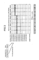
When addresses are aligned according to the size of the specified data as shown in Fig. 2, the values of any bits are not cared when the specified size is Byte in the low-order bits in the address of [2:0]. Further, only the value of the bit of [0] is required to be zero when the specified size is Half word. Moreover, the values of bits of [1] and [0] are required to be zero when the specified size is Word. In addition, the values of all the bits are required to be zero when the specified size is Double word. Therefore, the case where the addresses are aligned differently from those according to the size of the specified data indicates a case where the conditions shown in Fig. 2 are not met.
For example, as shown in Fig. 3, when the address of data to be read or written is 32'h00000015 and the specified data size is of 8 bytes, the value of a bit of [2] in the address is 1, that of a bit of [1] is zero, and that of a bit of [0] is 1. The above states do not meet the conditions that are required as shown in Fig. 2 when the data size is of 8 bytes. Accordingly, the example shown in Fig. 3 signifies that the addresses are not aligned with respect to the data size of 8 bytes . In such a case, the 8-byte addresses starting from an address of 32'h00000015 cross over an 8-byte boundary set in the memory.
In the example in Fig. 3, the 8-byte boundary includes, for example, a boundary between 32'h00000007 and 32'h00000008, that between 32'h0000000 F and 32'h00000010, and that between 32'h00000017 and 32'h00000018.
Generally, addresses for data reading or data writing are apparent only at execution of software. Therefore, the previously-considered information processing device has had a problem that longer processing time for data reading or data writing is required when the addresses of data to be read or written are not aligned as described above, because reading or writing of data with a 1-byte size as a minimum unit is required to be executed eight times when the data size is of 8 bytes.
It is desirable to provide a device and a method for information processing by which data reading or data writing can be executed by one-time memory access even when addresses are aligned differently from those according to the size of data specified at the data reading or the data writing.
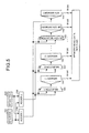
An information processing device according to an embodiment of one aspect of the present invention has the following configuration. As shown in Fig. 4, a memory consists of N memory areas 141 to 144 and has a M × N-bit write width (M and N are natural numbers) . A first address adder 124 (adder 1) generates target addresses for writing of data based on values stored in a first register 121 (register 1) and a second register 122 (register 2) . Further, a second address adder 134 (adder 2) generates addresses by adding N to the generated target addresses.
A first to a (N-1)th selectors 151 to 153 provided before the first to the (N-1) th memory areas 141 to 143 select either the address generated in the first address adder 124, or the address generated in the second address adder 134, and supplies the selected address to the memory areas 141 to 143, respectively. Moreover, the address generated in the first address adder 124 is supplied to an Nth memory area 144. A write control circuit 125 generates write control signals based on the data sizes stored in a third register 123 (register 3), and the address generated by the first address adder 124 is supplied to each memory area 141 to 144.
According to such an embodiment of the invention, even when the size of write data crosses over an M × N boundary, necessary data can be written at one-time memory-access by switching the addresses to be supplied into the memory corresponding to the target addresses for write and the sizes of the write data.
An information processing device according to an embodiment of another aspect of the present invention has the following configuration. As shown in Fig. 5, a memory consists of N memory areas 141 to 144 and has a M × N-bit read width (M and N are natural numbers) . The first address adder 124 generates addresses in which read data is stored based on values stored in the first register 121 and the second register 122. Further, the second address adder 134 generates addresses by adding N to the generated addresses.
The first to the (N-1)th selectors 151 to 153 provided before the first to the (N-1) th memory areas 141 to 143 select either the address generated in the first address adder 124, or the address generated in the second address adder 134, and supplies the selected address to the memory areas 141 to 143, respectively. Moreover, the address generated by the first address adder 124 is supplied to an Nth memory area 144.
According to such an embodiment of the invention, even when the size for data reading crosses over an M × N boundary, necessary data can be read at one-time memory-access by switching the addresses to be supplied into the memory corresponding to the addresses of storage locations and the sizes of the data to be read.
Reference will now be made, by way of example, to the accompanying drawings, in which:
  • Fig. 1 is a block diagram showing the configuration for data reading or data writing in a previously-considered information processing device;
  • Fig. 2 is a table showing relations between the values of low-order bits in addresses and data sizes in the previously-considered information processing device when the addresses are aligned according to a specified data size;
  • Fig. 3 is a schematic diagram for explaining the case where the addresses are aligned differently from those according to the specified data size;
  • Fig. 4 is a block diagram showing a principle of a configuration for data writing in an information processing device according to an embodiment of the present invention;
  • Fig. 5 is a block diagram showing a principle of a configuration for data reading in an information processing device according to an embodiment of the present invention;
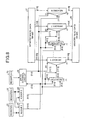
  • Fig. 6 is a block diagram showing a configuration for data reading or data writing in an information processing device according to an embodiment of the present invention;
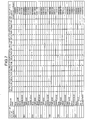
  • Fig. 7 is a table showing truth values of various kinds of signals in an information processing device according to the embodiment; and
  • Fig. 8 is a block diagram showing another example of the configuration for data reading or data writing in an information processing device according to the embodiment.
  • Embodiments of the present invention will be described in detail below with reference to the drawings. The description will be given, for convenience, by taking up an example of a cache memory that has a read or write size of a range between a maximum 64-bit width and a minimum 8-bit one, and a capacity of 8 kilobytes according to a direct map method, but other embodiments of the present invention are not limited to the above example . Here, the cache memory is composed of eight memory areas with a width of 8 bits, and has a memory space, for example, shown in Fig.3. Moreover, a address space is assumed to be of 32 bits, and the read and write bus-width is assumed to be of 8 bytes.
    Fig. 6 is a block diagram showing a configuration for data reading or data writing in an information processing device according to an embodiment of the present invention. As shown in Fig. 6, the information processing device comprises first to third registers 21, 22, 23, first and second address adders 24, 34, a write control circuit 25, eight memory areas 41 to 47 and 48, and seven selectors 51 to 57. Here, five memory areas and five selectors are omitted in Fig. 6.
    An address representing a storage location of read data and an address representing a target address for write of data are obtained, based on values stored in the first register 21 (register 1) and the second register 22 (register 2). For example, the first register 21 stores a base address for the address representing the storage location of the read data, or a base address for the address representing the target for write of the data. Further, for example, the second register 22 stores offsets from the base addresses. The third register 23 (register 3) stores the sizes of write data.
    The first address adder 24 (adder 1) adds the value stored in the first register 21 and the value stored in the second register 22 to generate an address indicating a storage location of read data, or an address indicating a target for write of data. The values of low-order 3 bits of [2:0] in a 13-bit address of [12:0] generated in the first address adder 24 are supplied to the write control circuit 25, and the selectors 51 to 57. The values of subsequent low-order 3bitsof [5:3] are supplied to the selectors 51 to 57. Moreover, the values of 10 bits of [12:3], of the address generated by the first address adder 24, are supplied to the eighth memory area 48.
    The second address adder 34 adds the values stored in the first register 21 and the values stored in the second register 22, and further adds 8 to the addition result . That is, an address obtained by adding 8 to the address generated in the first address adder 24 is generated. Only the values of bits of [5:3] in the address generated by the second address adder 34 is supplied to the selectors 51 to 57.
    Each of the selectors 51 to 57 selects either the values of bits of [5:3] supplied from the first address adder 24, or those of bits of [5:3] supplied from the second address adder 34 to output the selected values. In such a case, the selectors 51 to 57 select the above values, based on the values of the bits of [2:0] supplied from the first address adder 24. The values of bits of [5:3] which have been output from the selectors 51 to 57 are combined with the values of high-order 7 bits of [12:6], of the addresses generated by the first address adder 24 is supplied as 10-bit address of [12:3] to the first to the seventh memory areas 41 to 47.
    It has been assumed that the address space is of 32 bits, but high-order bits of [31:13] of the address are not always necessary, and 10 bits of [12:3] are enough because the first to the eighth memory areas 41 to 48 form the cache memory.
    The write control circuit 25 generates a write control signals of [7:0] for the first to the eighth memory areas 41 to 48, based on the size of write data supplied from the third register 23 and the values of bits of [2:0] supplied from the first address adder 24. The write control signal of each bit of [0] to [7] forming [7:0] is supplied to each of corresponding memory areas 41 to 48, respectively. In each of the memory areas 41 to 48 at data writing, memory write data 27 of [63:0] is written into the above address of [12:3], based on the write control signals supplied from the write control circuit 25. On the other hand, at data reading, data of a predetermined size, for example, of 64 bits is read from the above-described address of [12:3] as memory read data 28.
    Subsequently, relations among the values of bits of [2:0] output from the first address adder 24, a memory access size (specified size) , outputs of the first to the seventh selector 51 to 57, and the values of the write control signals of [7:0] output from the write control circuit 25, will be described below.
    Fig. 7 is a table showing the above relations. The access size includes Byte (8 bits), Half word (16 bits), Word (32 bits), and Double word (64 bits). In Fig. 7, fields of "Output of selector 1" to "Output of selector 7" represent that the first to the seventh selectors 51 to 57 select either [5:3] supplied from the first address adder 24 or [5:3] supplied from the second address adder 34, respectively. "1" shows that the output of the first address adder 24 is selected, and "2" shows that the output of the second address adder 34 is selected. Furthermore, data is written into memory areas corresponding to the bit of "1" in the field of "Output [7:0] of write control circuit".
    When all the values of bits of [2:0] output from the first address adder 24 are zero, all the selectors 51 to 57 select the values of [5:3] which have been supplied by the first address adder 24. Further, when the access size is Byte, only the value of a bit of [7] becomes 1, and the values of each bit of [6] to [0] become zero with regard to the write control signal. Accordingly, referring to the example in Fig. 3, 1-byte memory write data 27 are written into 1-byte address locations starting from an address of 32'h00000000, 32'h00000008, 32'h00000010, or 32'h00000018 (hereinafter, called as an address such as 32'h00000000). Alternatively, data corresponding to consecutive 8-byte address locations starting from an address such as 32'h00000000 is read as memory read data 28. In the above data, 1-byte data starting from an address such as 32'h00000000 is actually used for processing in a processor.
    When the access size is of the half word, only the values of bits of [7] and [6] become 1, and the values of each bit of [5] to [0] become zero with regard to the write control signal. Therefore, referring to the example in Fig. 3, 2-byte memory write data 27 are written into consecutive 2-byte address locations starting from an address such as 32'h00000000.
    At data reading, data corresponding to consecutive 8-byte address locations starting from an address such as 32'h00000000 is read as memory read data 28. In the above data, consecutive 2-byte data starting from an address such as 32'h00000000 is actually used for processing in the processor.
    When the access size is Word, the values of each bit of [7] to [4] become 1, and the values of each bit of [3] to [0] become zero with regard to the write control signal. Therefore, referring to the example in Fig. 3, 4-byte memory write data 27 are written into consecutive 4-byte address locations starting from an address such as 32'h00000000.
    At data reading, data corresponding to consecutive 8-byte address locations starting from an address such as 32'h00000000 is read as memory read data 28. In the above data, consecutive 4-byte data starting from an address such as 32'h00000000 are actually used for processing in the processor.
    When the access size is Double word, the values of all the bits of [7] to [0] become 1 with regard to the write control signal. Therefore, referring to the example in Fig. 3, 8-byte memory write data 27 are written into consecutive 8-byte address locations starting from an address such as 32'h00000000.
    At data reading, data corresponding to consecutive 8-byte address locations starting from an address such as 32'h00000000 are read as memory read data 28, and are used for processing in the processor.
    When, in 3 bits of [2:0] which have been output from the first address adder 24, only the value of a bit of [0] is 1 and the values of the other bits are zero, only the first selector 51 selects the values of [5:3] supplied from the second address adder 34, and the second selector to the seventh selector 57 select the values of [5:3] supplied from the first address adder 24. Further, when the access size is Byte, only the value of a bit of [6] becomes 1, and the values of the other bits become zero with regard to the write control signal. Accordingly, referring to the example in Fig. 3, 1-byte memory write data 27 are written into 1-byte address locations starting from an address such as 32'h00000001, 32'h00000009, 32'h00000011, or 32'h00000019 (hereinafter, called as an address such as 32'h00000001).
    At data reading, 8-byte data are read as memory read data 28. More specifically, the 8-byte data correspond to consecutive 7-byte address locations starting from an address such as 32'h00000001 and 1-byte address locations of an address such as 32'h00000000 that are determined by the next base address after an 8-byte boundary set in the memory. In the above data, 1-byte data starting from an address such as 32'h00000001 are used for processing in the processor.
    When the access size is Half word, only the values of bits of [6] and [5] become 1, and the values of the other bits become zero with regard to the write control signal. Therefore, referring to the example in Fig. 3, 2-byte memory write data 27 are written into 2-byte address locations starting from an address such as 32'h00000001.
    At data reading, 8-byte data are read as memory read data 28. More specifically, the 8-byte data correspond to consecutive 7-byte address locations starting from an address such as 32'h00000001 and 1-byte address locations of an address such as 32'h00000000 that are determined by the next base address after the 8-byte boundary set in the memory, . In the above data, 2-byte data starting from an address such as 32'h00000001 are used for processing in the processor.
    When the access size is Word, the values of each bit of [6] to [3] become 1, and the values of the other bits become zero with regard to the write control signal. Therefore, referring to the example in Fig. 3, 4-byte memory write data 27 are written into 4-byte address locations starting from an address such as 32'h00000001.
    At data reading, 8-byte data are read as memory read data 28. More specifically, the 8-byte data correspond to consecutive 7-byte address locations starting from an address such as 32'h00000001 and 1-byte address locations of an address such as 32'h00000000 that are determined by the next base address after the 8-byte boundary set in the memory. In the above data, 4-byte data starting from an address such as 32'h00000001 are used for processing in the processor.
    When the access size is Double word, the values of all the bits of [7] to [0] become 1 with regard to the write control signal. Therefore, referring to the example in Fig. 3, 8-byte memory write data 27 are written into consecutive 7-byte address locations starting from an address such as 32'h00000001 and 1-byte address locations of an address such as 32'h00000000, which are determined by the next base addresses after the 8-byte boundary set in the memory.
    At data reading, 8-byte data are read as memory read data 28. More specifically, the 8-byte data correspond to consecutive 7-byte address locations starting from an address such as 32'h00000001 and 1-byte address locations of an address such as 32' h00000000 that are determined by the next base address after the 8-byte boundary set in the memory, and the read data are used for processing in the processor.
    When, in 3 bits of [2:0] which have been output from the first address adder 24, only the value of a bit of [1] is 1, and the values of the other bits are zero, the first selector 51 and the second selector select the values of [5:3] supplied from the second address adder 34, and the third to the sixth selectors, and the seventh selector 57 select the values of [5:3] supplied from the first address adder 24. Further, when the access size is Byte, only the value of a bit of [5] becomes 1, and the values of the other bits become zero with regard to the write control signal. Accordingly, referring to the example in Fig. 3, 1-byte memory write data 27 are written into 1-byte address locations starting from an address such as 32'h00000002, 32'h0000000A, 32'h00000012, or 32'h0000001A (hereinafter, called as an address of 32'h00000002).
    At data reading, 8-byte data are read as memory read data 28. More specifically, the 8-byte data correspond to consecutive 6-byte address locations starting from an address such as 32'h00000002, and consecutive 2-byte address locations starting from an address such as 32'h000000000 that are determined by the next base address after the 8-byte boundary set in the memory. In the above data, 1-byte data starting from an address such as 32'h00000002 are used for processing in the processor.
    When the access size is Half word, only the values of bits of [5] and [4] become 1, and the values of the other bits become zero with regard to the write control signal. Accordingly, referring to the example in Fig. 3,2-byte memory write data 27 are written into 2-byte address locations starting from an address such as 32'h00000002.
    At data reading, 8-byte data are read as memory read data 28. More specifically, the 8-byte data correspond to consecutive 6-byte address locations starting from an address such as 32'h00000002, and consecutive 2-byte address locations starting from an address such as 32'h000000000 that are determined by the next base address after the 8-byte boundary set in the memory. In the above data, 2-byte data starting from an address such as 32'h00000002 are used for processing in the processor.
    When the access size is Word, the values of each bit of [5] to [2] become 1, and the values of the other bits become zero with regard to the write control signal. Accordingly, referring to the example in Fig. 3,4-byte memory write data 27 are written into consecutive 4-byte address locations starting from an address such as 32'h00000002.
    At data reading, 8-byte data are read as memory read data 28. More specifically, the 8-byte data correspond to consecutive 6-byte address locations starting from an address such as 32'h00000002, and consecutive 2-byte address locations starting from an address such as 32'h000000000 that are determined by the next base address after the 8-byte boundary set in the memory. In the above data, 4-byte data starting from an address such as 32'h00000002 are used for processing in the processor.
    When the access size is Double word, the values of all the bits of [7] to [0] become 1 with regard to the write control signal. Therefore, referring to the example in Fig. 3, 8-byte memory write data 27 are written into consecutive 6-byte address locations starting from an address such as 32'h00000002, and consecutive 2-byte address locations starting from an address such as 32'h00000000 that are determined by the next base address after the 8-byte boundary set in the memory.
    At data reading, 8-byte data are read as memory read data 28. More specifically, the 8-byte data correspond to consecutive 6-byte address locations starting from an address such as 32'h00000002, and consecutive 2-byte address locations starting from an address such as 32'h00000000 that are determined by the next base address after the 8-byte boundary set in the memory, and are used for processing in the processor.
    When, in 3 bits of [2:0] which have been output from the first address adder 24, the values of bits of [1] and [0] are 1, and the values of the other bits are zero, the first selector 51, the second selector, and the third selector select the values of [5:3] supplied from the second address adder 34, and the fourth to the sixth selectors, and the seventh selector 57 select the values of [5:3] supplied from the first address adder 24. Further, when the access size is Byte, only the value of a bit of [4] becomes 1, and the values of the other bits become zero with regard to the write control signal. Accordingly, referring to the example in Fig. 3, 1-byte memory write data 27 are written into 1-byte address locations starting from an address such as 32'h00000003, 32'h0000000B, 32'h00000013, or 32'h0000001B (hereinafter, called as an address such as 32'h00000003)
    At data reading, 8-byte data are read as memory read data 28. More specifically, the 8-byte data correspond to consecutive 5-byte address locations starting from an address such as 32'h00000003, and consecutive 3-byte address locations starting from an address such as 32'h00000000 that are determined by the next base address after the 8-byte boundary set in the memory. In the above data, 1-byte data starting from an address such as 32'h00000003 are used for processing in the processor.
    When the access size is Half word, the values of all the bits of [4] and [3] become 1, and the values of the other bits become zero with regard to the write control signal. Accordingly, referring to the example in Fig. 3,2-byte memory write data 27 are written into consecutive 2-byte address locations starting from an address such as 32'h00000003.
    At data reading, 8-byte data are read as memory read data 28. More specifically, the 8-byte data correspond to consecutive 5-byte address locations starting from an address such as 32'h00000003, and consecutive 3-byte address locations starting from an address such as 32'h00000000 that are determined by the next base address after the 8-byte boundary set in the memory. In the above data, 2-byte data starting from an address such as 32'h00000003 are used for processing in the processor.
    When the access size is Word, the values of each bit of [4] to [1] become 1, and the values of the other bits become zero with regard to the write control signal. Accordingly, referring to the example in Fig. 3,4-byte memory write data 27 are written into consecutive 4-byte address locations starting from an address such as 32'h00000003.
    At data reading, 8-byte data are read as memory read data 28. More specifically, the 8-byte data correspond to consecutive 5-byte address locations starting from an address such as 32'h00000003, and consecutive 3-byte address locations of an address such as 32'h00000000 that are determined by the next base address after the 8-byte boundary set in the memory. In the above data, 4-byte data starting from an address such as 32'h00000003 are used for processing in the processor.
    When the access size is Double word, the values of all the bits of [7] to [0] become 1 with regard to the write control signal. Therefore, referring to the example in Fig. 3, 8-byte memory write data 27 are written into consecutive 5-byte address locations starting from an address such as 32'h00000003, and consecutive 3-byte address locations starting from an address such as 32'h00000000 that are determined by the next base address after the 8-byte boundary set in the memory.
    At data reading, 8-byte data are read as memory read data 28. More specifically, the 8-byte data correspond to consecutive 5-byte address locations starting from an address such as 32'h00000003, and consecutive 3-byte address locations starting from an address such as 32'h00000000 that are determined by the next base address after the 8-byte boundary set in the memory, and are used for processing in the processor.
    When, in 3 bits of [2:0] which have been output from the first address adder 24, only the value of a bit of [2] is 1, and the values of the other bits are zero, the first selector 51, and the second to the fourth selectors select the values of [5:3] supplied from the second address adder 34, and the fifth selector, the sixth selector, and the seventh selector 57 select the values of [5:3] supplied from the first address adder 24. Further, when the access size is Byte, only the value of a bit of [3] becomes 1, and the values of the other bits become zero with regard to the write control signal. Accordingly, referring to the example in Fig. 3, 1-byte memory write data 27 are written into 1-byte address locations starting from an address such as 32'h00000004, 32'h0000000C, 32'h00000014, or 32'h0000001C (hereinafter, called as an address such as 32'h00000004).
    At data reading, 8-byte data are read as memory read data 28. More specifically, the 8-byte data correspond to consecutive 4-byte address locations starting from an address such as 32'h00000004, and consecutive 4-byte address locations starting from an address such as 32'h00000000 that are determined by the next base address after the 8-byte boundary set in the memory. In the above data, 1-byte data starting from an address such as 32'h00000004 are used for processing in the processor.
    When the access size is Half word, only the values of bits of [3] and [2] become 1, and the values of the other bits become zero with regard to the write control signal. Accordingly, referring to the example in Fig. 3,2-byte memory write data 27 are written into consecutive 2-byte address locations starting from an address such as 32'h00000004.
    At data reading, 8-byte data are read as memory read data 28. More specifically, the 8-byte data correspond to consecutive 4-byte address locations starting from an address such as 32'h00000004, and consecutive 4-byte address locations of an address such as 32'h00000000 that are determined by the next base address after the 8-byte boundary set in the memory. In the above data, 2-byte data starting from an address such as 32'h00000004 are used for processing in the processor.
    When the access size is Word, only the values of each bit of [3] to [0] become 1, and the values of the other bits become zero with regard to the write control signal. Accordingly, referring to the example in Fig. 3,4-byte memory write data 27 are written into 4-byte address locations starting from an address such as 32'h00000004.
    At data reading, 8-byte data are read as memory read data 28. More specifically, the 8-byte data correspond to consecutive 4-byte address locations starting from an address such as 32'h00000004, and consecutive 4-byte address locations starting from an address such as 32'h00000000 that are determined by the next base address after the 8-byte boundary set in the memory. In the above data, 4-byte data starting from an address such as 32'h00000004 are used for processing in the processor.
    When the access size is Double word, the values of all the bits of [7] to [0] become 1 with regard to the write control signal. Therefore, referring to the example in Fig. 3, 8-byte memory write data 27 are written into consecutive 4-byte address locations starting from an address such as 32'h00000004, and consecutive 4-byte address locations starting from an address such as 32'h00000000 that are determined by the next base address after the 8-byte boundary set in the memory.
    At data reading, 8-byte data are read as memory read data 28. More specifically, the 8-byte data correspond to consecutive 4-byte address locations starting from an address such as 32'h00000004, and consecutive 4-byte address locations starting from an address such as 32'h00000000 that are determined by the next base address after the 8-byte boundary set in the memory, and are used for processing in the processor.
    When, in 3 bits of [2:0] which have been output from the first address adder 24, the values of bits of [2] and [0] are 1, and the value of a bit of [1] is zero, the first selector 51 and the second to the fifth selectors select the values of [5:3] supplied from the second address adder 34, and the sixth selector and the seventh selector 57 select the values of [5:3] supplied from the first address adder 24. Further, when the access size is Byte, only the value of a bit of [2] becomes 1, and the values of the other bits become zero with regard to the write control signal. Accordingly, referring to the example in Fig. 3, 1-byte memory write data 27 are written into 1-byte address locations starting from an address such as 32'h00000005, 32'h0000000D, 32'h00000015, or 32'h0000001D (hereinafter, called as an address such as 32'h00000005).
    At data reading, 8-byte data are read as memory read data 28. More specifically, the 8-byte data correspond to consecutive 3-byte address locations starting from an address such as 32'h00000005, and consecutive 5-byte address locations starting from an address such as 32'h00000000 that are determined by the next base address after the 8-byte boundary set in the memory. In the above data, 1-byte data starting from an address such as 32'h00000005 are used for processing in the processor.
    When the access size is Half word, only the values of bits of [2] and [1] become 1, and the values of the other bits become zero with regard to the write control signal. Therefore, referring to the example in Fig. 3, 2-byte memory write data 27 are written into 2-byte address locations starting from an address such as 32'h00000005.
    At data reading, 8-byte data are read as memory read data 28. More specifically, the 8-byte data correspond to consecutive 3-byte address locations starting from an address such as 32'h00000005, and consecutive 5-byte address locations starting from an address such as 32'h00000000 that are determined by the next base address after the 8-byte boundary set in the memory. In the above data, 2-byte data starting from an address such as 32'h00000005 are used for processing in the processor.
    When the access size is Word, the values of each bit of [7] and [2] to [0] become 1, and the values of the other bits become zero with regard to the write control signal. Therefore, referring to the example in Fig. 3, 4-byte memory write data 27 are written into consecutive 3-byte address locations starting from an address such as 32'h00000005, and 1-byte address locations starting from an address such as 32'h00000000 that are determined by the next base address after the 8-byte boundary set in the memory.
    At data reading, 8-byte data are read as memory read data 28. More specifically, the 8-byte data correspond to consecutive 3-byte address locations starting from an address such as 32'h00000005, and consecutive 5-byte address locations starting from an address such as 32'h00000000 that are determined by the next base address after the 8-byte boundary set in the memory. In the above data, consecutive 3-byte data starting from an address such as 32'h00000005 and the next 1-byte data starting from an address such as 32'h00000000 are used for processing in the processor.
    When the access size is Double word, the values of all the bits of [7] to [0] become 1 with regard to the write control signal. Therefore, referring to the example in Fig. 3, 8-byte memory write data 27 are written into consecutive 3-byte address locations starting from an address such as 32'h00000005, and consecutive 5-byte address locations starting from an address such as 32'h00000000 that are determined by the next base address after the 8-byte boundary set in the memory.
    At data reading, 8-byte data are read as memory read data 28. More specifically, the 8-byte data correspond to consecutive 3-byte address locations starting from an address such as 32'h00000005, and consecutive 5-byte address locations starting from an address such as 32'h00000000 that are determined by the next base address after the 8-byte boundary set in the memory, and are used for processing in the processor. In the example shown in Fig. 3, the 8-byte data corresponds to consecutive 3-byte address locations of 32'H00000015 to 32'H00000017, and consecutive 5-byte address locations of 32'H00000018 to 32'H0000001C, which are the next base address.
    When, in 3 bits of [2:0] which have been output from the first address adder 24, the values of bits of [2] and [1] are 1, and the value of a bit of [0] is zero, the first selector 51, and the second to the sixth selectors select the values of [5:3] supplied from the second address adder 34, and the seventh selector 57 selects the values of [5:3] supplied from the first address adder 24. Further, when the access size is Byte, only the value of a bit of [2] becomes 1, and the values of the other bits become zero with regard to the write control signal. Accordingly, referring to the example in Fig. 3, 1-byte memory write data 27 are written into 1-byte address locations starting from an address such as 32'h00000006, 32'h0000000E, 32'h00000016, and 32'h0000001E (hereinafter, called as an address such as 32'h00000006).
    At data reading, 8-byte data are read as memory read data 28. More specifically, the 8-byte data correspond to consecutive 2-byte address locations starting from an address such as 32'h00000006, and consecutive 6-byte address locations starting from an address such as 32'h00000000 that are determined by the next base address after the 8-byte boundary set in the memory. In the above data, 1-byte data starting from an address such as 32'h00000006 are used for processing in the processor.
    When the access size is Half word, only the values of bits of [1] and [0] become 1, and the values of the other bits become zero with regard to the write control signal. Accordingly, referring to the example in Fig. 3,2-byte memory write data 27 are written into consecutive 2-byte address locations starting from an address such as 32'h00000006.
    At data reading, 8-byte data are read as memory read data 28. More specifically, the 8-byte data correspond to consecutive 2-byte address locations starting from an address such as 32'h00000006, and consecutive 6-byte address locations starting from an address such as 32'h00000000 that are determined by the next base address after the 8-byte boundary set in the memory. In the above data, 2-byte data starting from an address such as 32'h00000006 are used for processing in the processor.
    When the access size is Word, the values of each bit of [7], [6], [1], and [0] become 1, and the values of the other bits become zero with regard to the write control signal. Therefore, referring to the example in Fig. 3, 4-byte memory write data 27 are written into consecutive 2-byte address locations starting from an address such as 32'h00000006, and consecutive 2-byte address locations starting from an address such as 32'h00000000 that are determined by the next base address after the 8-byte boundary set in the memory.
    At data reading, 8-byte data are read as memory read data 28. More specifically, the 8-byte data correspond to consecutive 2-byte address locations starting from an address such as 32'h00000006, and consecutive 6-byte address locations from an address such as 32'h00000000 that are determined by the next base address after the 8-byte boundary set in the memory. In the above data, 2-byte data starting from an address such as 32'h00000006 and 2-byte data starting from an address such as 32'h00000000 are used for processing in the processor.
    When the access size is Double word, the values of all the bits of [7] to [0] become 1 with regard to the write control signal. Therefore, referring to the example in Fig. 3, 8-byte memory write data 27 are written into consecutive 2-byte address locations starting from an address such as 32'h00000006, and consecutive 6-byte address locations starting from an address such as 32'h00000000 that are determined by the next base address after the 8-byte boundary set in the memory.
    At data reading, 8-byte data are read as memory read data 28. More specifically, the 8-byte data correspond to consecutive 2-byte address locations starting from an address such as 32'h00000006, and consecutive 6-byte address locations starting from an address such as 32'h00000000 that are determined by the next base address after the 8-byte boundary set in the memory, and are used for processing in the processor.
    When, the values of each bit of [2:0] which have been output from the first address adder 24 are 1, all the selectors 51 to 57 select the values of [5:3] supplied from the second address adder 34. When the access size is Byte, only the value of a bit of [0] becomes 1, and the values of the other bits become zero with regard to the write control signal. Accordingly, referring to the example in Fig. 3, 1-byte memory write data 27 are written into 1-byte address locations starting from an address such as 32'h00000007, 32'h0000000F, 32'h00000017, or 32'h0000001F (hereinafter, called as an address such as 32'h00000007).
    At data reading, 8-byte data are read as memory read data 28. More specifically, the 8-byte data correspond to 1-byte address locations starting from an address such as 32'h00000007, and consecutive 7-byte address locations starting from an address such as 32'h00000000 that are determined by the next base address after the 8-byte boundary set in the memory. In the above data, 1-byte data starting from an address such as 32'h00000007 are used for processing in the processor.
    When the access size is Half word, only the values of bits of [7] and [0] become 1, and the values of the other bits become zero with regard to the write control signal. Therefore, referring to the example in Fig. 3, 2-byte memory write data 27 are written into 1-byte address locations starting from an address such as 32'h00000007, and 1-byte address locations starting from an address such as 32'h00000000 that are determined by the next base address after the 8-byte boundary set in the memory.
    At data reading, 8-byte data are read as memory read data 28. More specifically, the 8-byte data correspond to 1-byte address locations starting from an address such as 32'h00000007, and consecutive 7-byte address locations starting from an address such as 32'h00000000 that are determined by the next base address after the 8-byte boundary set in the memory. In the above data, 1-byte data starting from an address such as 32'h00000007 and the next 1-byte data starting from an address such as 32'h00000000 are used for processing in the processor.
    When the access size is Word, the values of bits of [7] to [5], and [0] become 1, and the values of the other bits become zero with regard to the write control signal. Therefore, referring to the example in Fig. 3, 4-byte memory write data 27 are written into 1-byte address locations starting from an address such as 32' h00000007, and consecutive 3-byte address locations starting from an address such as 32'h00000000 that are determined by the next base address after the 8-byte boundary set in the memory.
    At data reading, 8-byte data are read as memory read data 28. More specifically, the 8-byte data correspond to 1-byte address locations starting from an address such as 32'h00000007, and consecutive 7-byte address locations starting from an address such as 32'h00000000 that are determined by the next base address after the 8-byte boundary set in the memory. In the above data, 1-byte data starting from an address such as 32'h00000007 and the next 3-byte data starting from an address such as 32'h00000000 are used for processing in the processor.
    When the access size is Double word, the values of all the bits of [7] to [0] become 1 with regard to the write control signal. Therefore, referring to the example in Fig. 3,8-byte memory write data 27 are written into 1-byte address locations starting from an address such as 32'h00000007, and consecutive 7-byte address locations starting from an address such as 32'h00000000 that are determined by the next base address after the 8-byte boundary set in the memory.
    At data reading, 8-byte data are read as memory read data 28. More specifically, the 8-byte data correspond to 1-byte address locations starting from an address such as 32'h00000007, and consecutive 7-byte address locations starting from an address such as 32'h00000000 that are determined by the next base address after the 8-byte boundary set in the memory, and are used for processing in the processor.
    According to the above embodiment, even when write data cross over the 8-byte boundary, necessary data can be written at one-time memory-access by switching the addresses to be supplied to the memory corresponding to a target address for write, and the size of write data.
    According to the above embodiment, even when the size of data to be read from the memory cross over the 8-byte boundary, necessary data can be read at one-time memory-access by switching the addresses to be supplied to the memory corresponding to an address at which read data is stored, and the size of the read data. Accordingly, even when the addresses are aligned differently from those according to the size of the data specified at data reading or data writing, the data can be read or written at one-time memory-access.
    An embodiment of the present invention may be applied not only to data reading or data writing from or into the cache memory with the above-described configuration, but also to address selection at data reading or data writing from or into a memory such as RAM or ROM. Moreover, an embodiment of the present invention may be applied not only to the cache memory according to the direct map method, but also to a cache memory according to a set associative method.
    The numerical values concerning the above-described addresses, sizes, and the like are only one example, and various kinds of modifications may be executed. although the above block size has been assumed to be of 64 bytes for description in the above-described embodiment, the block size of the cache memory may be of any size except for 64 bytes. In such a case, the address selected by each selector and the bit width of the output of the second address adder may be increased or decreased according to the size of the block.
    Fig. 8 shows a configuration in which the block size of a cache memory is of 128 bytes. A second address adder 62 supplies the values of bits of [6:3] in generated addresses to selectors 71 to 77 . A first address adder 61 also supplies the values of bits of [6:3] in the generated addresses to the selectors 71 to 77. The other components are the same as those of the above-described configuration in which the block size is of 64 bytes.
    According to an embodiment of the present invention, even when the size of write data cross over an M × N boundary, necessary data can be written at one-time memory access by switching addresses to be supplied to a memory, based on a target addresses for write and a size of the write data.
    Even when the size of read data cross over the M × N-bit boundary, necessary data can be read at one-time memory access by switching addresses to be supplied to the memory, based on an address at which the read data have been stored and the size of the read data. Accordingly, it is possible to obtain the device and method for information processing bywhichdatacanbereadorwrittenatone-timememory-access, even when addresses are aligned differently from those according to the size of the data specified at data reading or data writing.
    Although the invention has been described with respect to a specific embodiment for a complete and clear disclosure, the appended claims are not to be thus limited but are to be construed as embodying all modifications and alternative constructions that may occur to one skilled in the art which fairly fall within the basic teaching herein set forth.

    Claims (10)

    1. An information processing device provided with a memory consisting of N memory areas with a M-bit width and having a M × N-bit write width where M and N are natural numbers, the information processing device comprising:
      a first register that stores first data to generate addresses;
      a second register that stores second data to generate addresses;
      a third register that stores write sizes;
      a first address adder that generates a first address, based on the data stored in the first register and the data stored in the second register;
      a second address adder that generates a second address by adding N to the first address;
      a write control circuit that generates write control signals for the N memory areas, based on the first address and the write sizes;
      (N-1) selectors that select either the first address or the second address according to the first address;
      the (N-1) memory areas of the first to the (N-1)th memory areas into which data is written, based on the addresses supplied from the selectors and the write control signals; and
      the Nth memory area into which data is written, based on the first address and the write control signals.
    2. An information processing device provided with a memory consisting of N memory areas with a M-bit width and having a M × N-bit write width where M and N are natural numbers, the information processing device comprising:
      a first register that stores first data to generate addresses;
      a second register that stores second data to generate addresses;
      a third register that stores write sizes;
      a first address adder that generates a first address, based on the data stored in the first register and the data stored in the second register;
      a second address adder that generates a second address by adding N to the first address;
      (N-1) selectors that select either the first address or the second address according to the first address;
      the (N-1) memory areas of the first to the (N-1)th memory areas from which data is read, based on the addresses supplied from the selectors; and
      the Nth memory area from which data is read, based on the first address.
    3. An information processing device provided with a memory consisting of N memory areas with a M-bit width and having a M × N-bit write width where M and N are natural numbers, the information processing device comprising:
      a first register that stores first data to generate addresses;
      a second register that stores second data to generate addresses;
      a third register that stores write sizes;
      a first address adder that generates a first address, based on the data stored in the first register and the data stored in the second register;
      a second address adder that generates a second address by adding N to the first address;
      a write control circuit that generates write control signals for the N memory areas, based on the first address and the write sizes;
      (N-1) selectors that select either the first address or the second address according to the first address;
      the (N-1) memory areas of the first to the (N-1)th memory areas into which data is written based on the addresses supplied from the selectors and the write control signals, or from which data is read based on the addresses supplied from the selectors; and
      the Nth memory area into which data is written based on the first address and the write control signals, or from which data is read based on the first address.
    4. The information processing device according to claim 1, 2 or 3, wherein
         the first address adder adds the data stored in the first register to the data stored in the second register to generate the first address.
    5. The information processing device according to any preceding claim, wherein
         the second address adder adds the data stored in the first register to the data stored in the second register, and further adds N to a result of the addition to generate the second address.
    6. The information processing device according to any preceding claim, wherein, when integers represented by low-order 3 bits in the first address are K in the case of N = 8,
         all the selectors select the first address when K = 0;
         the first to the K-th selectors select the second address, and the (K+1)th to the seventh selectors select the first address, when 1 ≤ K ≤ 6; and
         all the selectors select the second address when K = 7.
    7. The information processing device according to any preceding claim, wherein, when integers represented by low-order 3 bits in the first address are K in the case of N = 8 and the write sizes are of J-bytes,
         the write control circuit allows
            the (K + 1)th to the (K + J)th memory areas to be in a writable state when 1 ≤ (K + J) ≤ 8, and
            the (K + 1)th to the eighth memory areas, and the first to the (K + J-8)th memory areas to be in a writable state when (K + J) ≥ 9.
    8. The information processing device according to any preceding claim, wherein the memory is a cache memory.
    9. An information processing method in an information processing device provided with a memory consisting of N memory areas with a M-bit width and having a M × N-bit write width where M and N are natural numbers, the information processing method comprising steps of:
      inputting first data and second data to generate addresses, and write sizes;
      generating a first address based on the first data and the second data;
      generating a second address by adding N to the first address;
      generating write control signals for N of the memory areas based on the first address and the write sizes;
      selecting either the first address or the second address according to the first address; and
      writing data into the (N-1) memory areas of the first to the (N-1)th memory areas based on the address selected in the selection step and the write control signals, and writing data into the Nth memory area based on the first address and the write control signals.
    10. An information processing method in an information processing device provided with a memory consisting of N memory areas with a M-bit width and having a M × N-bit write width where M and N are natural numbers, the information processing method comprising steps of:
      inputting first data and second data to generate addresses, and write sizes;
      generating a first address based on the first data and the second data;
      generating a second address by adding N to the first address;
      generating write control signals for N of the memory areas based on the first address and the write sizes;
      selecting either the first address or the second address according to the first address;
      writing data into the (N-1) memory areas of the first to the (N-1)th memory areas based on the address selected in the selection step and the write control signals, and writing data into the Nth memory area based on the first address and the write control signals; and
      reading data from the (N-1) memory areas of the first to the (N-1)th memory areas based on the address selected in the selection step, and reading data from the Nth memory area based on the first address.
    EP02258549A 2001-12-28 2002-12-11 Device and method for information processing Withdrawn EP1324202A3 (en)

    Applications Claiming Priority (2)

    Application Number Priority Date Filing Date Title
    JP2001399389 2001-12-28
    JP2001399389A JP2003196156A (en) 2001-12-28 2001-12-28 Information processing apparatus and information processing method

    Publications (2)

    Publication Number Publication Date
    EP1324202A2 true EP1324202A2 (en) 2003-07-02
    EP1324202A3 EP1324202A3 (en) 2004-01-02

    Family

    ID=19189466

    Family Applications (1)

    Application Number Title Priority Date Filing Date
    EP02258549A Withdrawn EP1324202A3 (en) 2001-12-28 2002-12-11 Device and method for information processing

    Country Status (3)

    Country Link
    US (1) US6931508B2 (en)
    EP (1) EP1324202A3 (en)
    JP (1) JP2003196156A (en)

    Cited By (3)

    * Cited by examiner, † Cited by third party
    Publication number Priority date Publication date Assignee Title
    EP1569124A1 (en) * 2004-02-26 2005-08-31 Matsushita Electric Industrial Co., Ltd. Memory interface and data processing
    FR2884002A1 (en) * 2005-04-01 2006-10-06 St Microelectronics Sa Bit symbol addressing method for use in memory bank of processing device, involves shifting symbol bits during reading or writing operation of symbols in memory bank based on value of pointer in read or written bit word
    CN101681502B (en) * 2006-11-09 2012-11-14 高通股份有限公司 Pixel Cache Memory for 3D Graphics Circuits

    Families Citing this family (2)

    * Cited by examiner, † Cited by third party
    Publication number Priority date Publication date Assignee Title
    US20060230198A1 (en) * 2005-03-30 2006-10-12 Kabushiki Kaisha Toshiba Data processing circuit, data processing method and image forming apparatus
    CN116431315B (en) * 2023-06-07 2023-08-29 成都登临科技有限公司 Batch processing task processing method and device, electronic equipment and storage medium

    Family Cites Families (7)

    * Cited by examiner, † Cited by third party
    Publication number Priority date Publication date Assignee Title
    JPH01175649A (en) * 1987-12-29 1989-07-12 Oki Electric Ind Co Ltd Micro processor
    JP2722523B2 (en) * 1988-09-21 1998-03-04 日本電気株式会社 Instruction prefetch device
    JPH0553920A (en) * 1991-08-26 1993-03-05 Toshiba Corp Structured address generator
    JPH06332792A (en) * 1993-05-21 1994-12-02 Mitsubishi Electric Corp Data processor, data reading control circuit thereof and data writing control circuit
    US5813045A (en) * 1996-07-24 1998-09-22 Advanced Micro Devices, Inc. Conditional early data address generation mechanism for a microprocessor
    US6502177B1 (en) * 1999-12-02 2002-12-31 Intel Corporation Single cycle linear address calculation for relative branch addressing
    JP2002236616A (en) * 2001-02-13 2002-08-23 Fujitsu Ltd Cache memory system

    Cited By (3)

    * Cited by examiner, † Cited by third party
    Publication number Priority date Publication date Assignee Title
    EP1569124A1 (en) * 2004-02-26 2005-08-31 Matsushita Electric Industrial Co., Ltd. Memory interface and data processing
    FR2884002A1 (en) * 2005-04-01 2006-10-06 St Microelectronics Sa Bit symbol addressing method for use in memory bank of processing device, involves shifting symbol bits during reading or writing operation of symbols in memory bank based on value of pointer in read or written bit word
    CN101681502B (en) * 2006-11-09 2012-11-14 高通股份有限公司 Pixel Cache Memory for 3D Graphics Circuits

    Also Published As

    Publication number Publication date
    JP2003196156A (en) 2003-07-11
    US20030126402A1 (en) 2003-07-03
    EP1324202A3 (en) 2004-01-02
    US6931508B2 (en) 2005-08-16

    Similar Documents

    Publication Publication Date Title
    KR100241049B1 (en) Element Selection Mechanisms for Vector Processors
    US5918252A (en) Apparatus and method for generating a modulo address
    US4675809A (en) Data processing system for floating point data having a variable length exponent part
    US4615006A (en) Physical address developing unit
    US6560691B2 (en) Modulus address generator and method for determining a modulus address
    US5459847A (en) Program counter mechanism having selector for selecting up-to-date instruction prefetch address based upon carry signal of adder which adds instruction size and LSB portion of address register
    JPH0414385B2 (en)
    US6684267B2 (en) Direct memory access controller, and direct memory access control method
    EP0636986A2 (en) Address decoder with small circuit scale and address area expansion capability
    US6499099B1 (en) Central processing unit method and apparatus for extending general instructions with extension data of an extension register
    US6931508B2 (en) Device and method for information processing
    KR100764260B1 (en) How to Create Execution Instructions in Processing Systems
    US7308553B2 (en) Processor device capable of cross-boundary alignment of plural register data and the method thereof
    US20030033499A1 (en) Method and system for circular addressing with efficient memory usage
    US20030046516A1 (en) Method and apparatus for extending instructions with extension data of an extension register
    US4575796A (en) Information processing unit
    US5539900A (en) Information processing system
    US4975835A (en) Variable length data processing apparatus for consecutively processing variable-length data responsive to one instruction
    US5506747A (en) Provision of FIFO buffer in RAM
    US6886159B2 (en) Computer system, virtual machine, runtime representation of object, storage media and program transmission apparatus
    KR100301224B1 (en) Method for specifying a memory address for increasing the number of memory address locations available in a computer storing a high-precision number
    JP2005222519A (en) Access to bit value in data word stored in memory
    US6081869A (en) Bit-field peripheral
    US5708800A (en) High speed microprocessor for processing and transferring N-bits of M-bit data
    JP2023082311A (en) Arithmetic unit

    Legal Events

    Date Code Title Description
    PUAI Public reference made under article 153(3) epc to a published international application that has entered the european phase

    Free format text: ORIGINAL CODE: 0009012

    AK Designated contracting states

    Designated state(s): AT BE BG CH CY CZ DE DK EE ES FI FR GB GR IE IT LI LU MC NL PT SE SI SK TR

    AX Request for extension of the european patent

    Extension state: AL LT LV MK RO

    PUAL Search report despatched

    Free format text: ORIGINAL CODE: 0009013

    AK Designated contracting states

    Kind code of ref document: A3

    Designated state(s): AT BE BG CH CY CZ DE DK EE ES FI FR GB GR IE IT LI LU MC NL PT SE SI SK TR

    AX Request for extension of the european patent

    Extension state: AL LT LV MK RO

    17P Request for examination filed

    Effective date: 20040315

    17Q First examination report despatched

    Effective date: 20040521

    AKX Designation fees paid

    Designated state(s): DE FR GB

    STAA Information on the status of an ep patent application or granted ep patent

    Free format text: STATUS: THE APPLICATION IS DEEMED TO BE WITHDRAWN

    18D Application deemed to be withdrawn

    Effective date: 20090701