EP1324190A2 - Data processing system having a read-modify-write unit - Google Patents
Data processing system having a read-modify-write unit Download PDFInfo
- Publication number
- EP1324190A2 EP1324190A2 EP02028779A EP02028779A EP1324190A2 EP 1324190 A2 EP1324190 A2 EP 1324190A2 EP 02028779 A EP02028779 A EP 02028779A EP 02028779 A EP02028779 A EP 02028779A EP 1324190 A2 EP1324190 A2 EP 1324190A2
- Authority
- EP
- European Patent Office
- Prior art keywords
- modify
- data
- read
- write
- output
- Prior art date
- Legal status (The legal status is an assumption and is not a legal conclusion. Google has not performed a legal analysis and makes no representation as to the accuracy of the status listed.)
- Granted
Links
- 230000015654 memory Effects 0.000 claims abstract description 184
- 238000001514 detection method Methods 0.000 claims description 4
- 230000004044 response Effects 0.000 claims description 4
- 238000010586 diagram Methods 0.000 description 18
- 230000004048 modification Effects 0.000 description 10
- 238000012986 modification Methods 0.000 description 10
- 238000012360 testing method Methods 0.000 description 6
- 230000006870 function Effects 0.000 description 5
- 230000002411 adverse Effects 0.000 description 4
- 238000003780 insertion Methods 0.000 description 4
- 230000037431 insertion Effects 0.000 description 4
- 230000000903 blocking effect Effects 0.000 description 2
- 235000019800 disodium phosphate Nutrition 0.000 description 2
- XUIMIQQOPSSXEZ-UHFFFAOYSA-N Silicon Chemical compound [Si] XUIMIQQOPSSXEZ-UHFFFAOYSA-N 0.000 description 1
- 238000009434 installation Methods 0.000 description 1
- 229910052710 silicon Inorganic materials 0.000 description 1
- 239000010703 silicon Substances 0.000 description 1
Images


Classifications
-
- G—PHYSICS
- G06—COMPUTING; CALCULATING OR COUNTING
- G06F—ELECTRIC DIGITAL DATA PROCESSING
- G06F9/00—Arrangements for program control, e.g. control units
- G06F9/06—Arrangements for program control, e.g. control units using stored programs, i.e. using an internal store of processing equipment to receive or retain programs
- G06F9/30—Arrangements for executing machine instructions, e.g. instruction decode
- G06F9/38—Concurrent instruction execution, e.g. pipeline, look ahead
-
- G—PHYSICS
- G06—COMPUTING; CALCULATING OR COUNTING
- G06F—ELECTRIC DIGITAL DATA PROCESSING
- G06F9/00—Arrangements for program control, e.g. control units
- G06F9/06—Arrangements for program control, e.g. control units using stored programs, i.e. using an internal store of processing equipment to receive or retain programs
- G06F9/30—Arrangements for executing machine instructions, e.g. instruction decode
- G06F9/30003—Arrangements for executing specific machine instructions
- G06F9/30007—Arrangements for executing specific machine instructions to perform operations on data operands
- G06F9/30018—Bit or string instructions
-
- G—PHYSICS
- G06—COMPUTING; CALCULATING OR COUNTING
- G06F—ELECTRIC DIGITAL DATA PROCESSING
- G06F9/00—Arrangements for program control, e.g. control units
- G06F9/06—Arrangements for program control, e.g. control units using stored programs, i.e. using an internal store of processing equipment to receive or retain programs
- G06F9/30—Arrangements for executing machine instructions, e.g. instruction decode
- G06F9/30003—Arrangements for executing specific machine instructions
- G06F9/3004—Arrangements for executing specific machine instructions to perform operations on memory
-
- G—PHYSICS
- G06—COMPUTING; CALCULATING OR COUNTING
- G06F—ELECTRIC DIGITAL DATA PROCESSING
- G06F9/00—Arrangements for program control, e.g. control units
- G06F9/06—Arrangements for program control, e.g. control units using stored programs, i.e. using an internal store of processing equipment to receive or retain programs
- G06F9/30—Arrangements for executing machine instructions, e.g. instruction decode
- G06F9/30003—Arrangements for executing specific machine instructions
- G06F9/30076—Arrangements for executing specific machine instructions to perform miscellaneous control operations, e.g. NOP
- G06F9/30087—Synchronisation or serialisation instructions
-
- G—PHYSICS
- G06—COMPUTING; CALCULATING OR COUNTING
- G06F—ELECTRIC DIGITAL DATA PROCESSING
- G06F9/00—Arrangements for program control, e.g. control units
- G06F9/06—Arrangements for program control, e.g. control units using stored programs, i.e. using an internal store of processing equipment to receive or retain programs
- G06F9/30—Arrangements for executing machine instructions, e.g. instruction decode
- G06F9/38—Concurrent instruction execution, e.g. pipeline, look ahead
- G06F9/3824—Operand accessing
- G06F9/3834—Maintaining memory consistency
-
- G—PHYSICS
- G06—COMPUTING; CALCULATING OR COUNTING
- G06F—ELECTRIC DIGITAL DATA PROCESSING
- G06F9/00—Arrangements for program control, e.g. control units
- G06F9/06—Arrangements for program control, e.g. control units using stored programs, i.e. using an internal store of processing equipment to receive or retain programs
- G06F9/30—Arrangements for executing machine instructions, e.g. instruction decode
- G06F9/38—Concurrent instruction execution, e.g. pipeline, look ahead
- G06F9/3885—Concurrent instruction execution, e.g. pipeline, look ahead using a plurality of independent parallel functional units
-
- G—PHYSICS
- G11—INFORMATION STORAGE
- G11C—STATIC STORES
- G11C7/00—Arrangements for writing information into, or reading information out from, a digital store
- G11C7/10—Input/output [I/O] data interface arrangements, e.g. I/O data control circuits, I/O data buffers
- G11C7/1006—Data managing, e.g. manipulating data before writing or reading out, data bus switches or control circuits therefor
Definitions
- the present invention relates to a system having a read-modify-write instructions installed therein.
- this invention relates to a system having a read-modify-write unit for performing read-modify-write operations, in addition to a central processing unit (abbreviated into CPU hereinafter).
- a central processing unit abbreviated into CPU hereinafter.
- the present invention relates to a system having a read-modify-write unit and also a digital signal processing (abbreviated into DSP hereinafter) unit, applicable, not only to CPU, but to a digital signal processor, etc., for performing a series of read-modify-write operations, like a CPU.
- DSP digital signal processing
- Microprocessors usually have a CPU incorporating an operation unit and a controller mounted on a silicon chip with LSI production technology.
- a computer system has such a microprocessor and memories connected thereto.
- Current microcomputers have memories also mounted on a microprocessor chip in which access is made between the microprocessor and memories via a bus interface unit (abbreviated into BIU hereinafter).
- BIU bus interface unit
- FIG. 30 Shown in FIG. 30 is known microprocessor architecture with a CPU 1, a memory 2 and a BIU 3 interposed therebetween.
- the CPU 1 executes a read bus cycle, a write bus cycle or a dummy bus cycle (not read nor write) to the memory 2 via the BIU 3.
- the BIU 3 receives a memory address, a read or a write request and write data, data to be written (in writing only) from the CPU 1, while passes read data, data read from the memory 2 to the CPU 1.
- FIG. 30 illustrates direct access to the memory 2 by the BIU 3.
- a memory controller (depending on the type of memory 2) may be provided between the BIU 3 and the memory 2, for read and write operations to the memory via the memory controller.
- a read-modify-write instruction is explained in detail. This instruction is a single instruction for CPU to execute a series of operations to read data from a memory, modify some or all bits of the read data and then rewrite the original data with the modified data in the memory.
- the read-modify-write instruction is used, for example, for bit manipulation to 1-bit data, such as, bit set, bit clear, bit inversion and bit logical operations (LOGICAL ORAND, NOR, etc) and also for bit field manipulation to 2-bit data or more, such as, arithmetic operations, logical operations, shift/rotation, insertion/replacement and clear/set.
- the most-significant bit and the least-significant bit are defined as bit 7 and bit 0, respectively, for a binary-digit data "10101010" stored in the 8-bit memory at a given address.
- Bit set to bit 2 replaces the value "0" of bit 2 in “10101010” with “1", thus "10101110” being written in the 8-bit memory.
- Bit clear to bit 7 clears the value "1" of bit 7 from “10101010” to have the value "0" for bit 7, thus "00101010” being written in the 8-bit memory.
- Bit inversion to bit 2 inverts the value "0" of bit 2 to “1" in “10101010", thus "10101110" being written in the 8-bit memory.
- Bit-LOGICAL OR operation to bit 2 applies a logical OR between the value "1" and “0” of bit 2 in “10101010” to have the result "1", thus "10101110” being written in the 8-bit memory.
- Bit field insertion of the value "1101" to 4-bit data "0101" of bits 6 to 3 in “10101010” replaces the value "1010” with "1101", thus "11101010” being written in the 8-bit memory.
- the discriminating data is then read from the memory for the apparatus A to execute a specific processing.
- the data is rewritten as "10” if it is "00” and restored, thus the apparatus A starts the processing. On the contrary, if the data is not "00", the apparatus A waits until the data changes to "00". When the apparatus A completes the processing, the data "00" is written in the memory.
- the apparatus B waits until the data changes to "00".
- the data "11” is then written so that the apparatus B can start a specific processing.
- the data "00” is also written when the apparatus B completes the processing.
- Read-modify-write processing is thus required for such a system in which the apparatus A and B are not allowed to simultaneously start processing so that processing will not be interrupt.
- the apparatus A starts processing even though the apparatus B is still in the processing mode.
- the apparatus A and B could suffer consequences in processing to be switched between the apparatus due to the interruption.
- the read-modify-write instruction includes bit manipulation, such as, bit set, bit clear, bit insertion, bit logical operations and bit inversion; bit field manipulation, such as, bit field insertion and bit field replacements; shift operations, such as, operation shift and logical shift; and add/subtract operations, such as, increment/decrement, as discussed above.
- Illustrated in FIG. 26 is instruction execution in a first known CISC (Complex Instruction Set Computer) processor with no pipelined processing.
- CISC Complex Instruction Set Computer
- a read-modify-write instruction (INSTRUCTION 2 in FIG. 26) requires at least 5-machine-cycle instruction-execution time for instruction fetch "F", instruction decode "D", memory read “rd”, data modify "mo", and memory write "wr".
- Illustrated in FIG. 27 is instruction execution in a second known CISC processor with pipelined processing.
- Some instructions in a read-modify-write instruction can be executed in parallel with other preceding and succeeding instructions although it requires 5-machine-cycle instruction-execution time for instruction fetch "F”, instruction decode "D”, memory read “rd”, data modify "mo” and memory write "wr".
- the F- and D-stages are executed while the preceding instructions “E” and “W” (INSTRUCTION 1) are being executed, and the mo- and wr-stages are executed while the succeeding instructions "F” and "D” (INSTRUCTION 3) are being executed. Therefore, the read-modify-write instruction is executed as if it runs for 3 machine cycles.
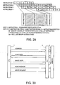
- FIG. 28 illustrates instruction execution in a third known RISC (Reduced Instruction Set Computer) processor with 5-stage pipelined processing.
- RISC Reduced Instruction Set Computer
- a pipeline has 5 stage of instruction fetch "F”, instruction decode "D”, computation execute "E”, memory access "M” and register write "W”.
- Modify processing is performed when the pipeline processing returns to the instruction-decode "D” and computation-execute "E” stages.
- the pipeline processing is performed in the order of instruction fetch "F”, instruction decode "D", computation execute "E”, memory access “M” with memory read, instruction decode "D”, computation execute "E” with data modify, memory access "M” with memory write and register write "W”.
- FIG. 29 illustrates read-modify-write processing for a fourth known processor that corresponds to the third known processor (FIG. 28) but to a memory with relatively slow read-write processing (such as a memory requiring 2 machine cycles for each of read and write).
- the read-modify-write instruction illustrated in FIG. 29 requires 5 machine cycles because a memory-access "M" stage requires at least 2 machine cycles.
- machine cycles for the read-modify-write instruction machine cycles for memory read + machine cycles for data modify + machine cycles for instruction execution.
- the read-modify-write instructions in the known first to the fourth known processors are relatively slow instructions requiring at least 3 to 5 machine cycles.
- the read-modify-write instruction requires longer execution time for slower processing-speed memories.
- Read-modify-write instructions such as bit manipulation
- bit manipulation usually occupy 10% to 15% of programs installed in electrical household appliances, such as air conditioners and digital camcorders, and AV (Audio-Visual) equipment, such as CD players, DVD players, TVs and VCRs. Instructions of slow execution speed but often used will cause low processor performances.
- a Read-modify-write-controlled system disclosed in Japanese Unexamined Patent publication No. 11-184761 has read-modify-write functions.
- the read-modify-write processing is performed simultaneously or in parallel to several memory banks. This is different from the present invention in which CPU instructions are executed in parallel with the preceding read-modify-write processing for higher throughput.
- Recent program-implemented equipment have become complex in processing. Moreover, there are demands for higher processing speed and/or lower power consumption. Higher system performance, or smaller number of clocks per instruction (abbreviated into CPI hereinafter) for each CPU instruction is strongly desired.
- CPI clocks per instruction
- Pipeline processing has been advanced for smaller CPI to meet the demands, however, obstructed by read-modify-write instructions such as bit manipulation due to 3 machine cycles or more in CPI.
- slow access-time memories affect CPI in read-modify-write operations.
- a purpose of the present invention is to provide a system with shorter apparent execution time for read-modify-write instructions.
- Another purpose of the present invention is to provide a system capable of executing a read-modify-write instruction in one machine cycle like other instructions.
- a data processing system includes: a central processing unit to decode and execute given instructions; a memory to store given data; a bus interface unit, provided between the central processing unit and the memory, to start a read bus cycle to read data from the memory, a write bus cycle to write data to the memory, or a dummy bus cycle (different from the read and write bus cycles); and a read-modify-write unit provided between the central processing unit and the bus interface unit.
- the read-modify-write unit has: a modify- requirements buffer to store modify requirements composed of modify data output from the central processing unit and an operation control signal; and a modify operation circuit to apply an operation processing to read data output from the bus interface unit with the modify data output from the modify-requirements buffer under the operation control signal to output an operation result to the bus interface unit, as write data.
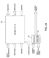
- FIG. 1 Disclosed first are a system architecture and its operational principle according to a first embodiment of the present invention with reference to FIGs. 1 to 3.
- the architecture of a processor according to a second embodiment, a modification to the first embodiment, will be disclosed next with reference to FIG. 4. Thereafter, the features of the present invention will be explained in accordance with several embodiments.
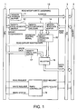
- FIG. 1 Disclosed now with respect to FIG. 1 is the system architecture according to the first embodiment of the present invention.
- the system at least includes a CPU 1 for decoding and executing several instructions; a memory 2 for storing given data; and a bus interface unit (abbreviated into BIU hereinafter) 3, interposed between the CPU 1 and the memory 2, for starting a read bus cycle to read data from the memory if an address from the CPU 1 is within address space of the memory 2, a write bus cycle to write data to the memory 2 if an address from the CPU 1 is within address space of the memory, or a dummy bus cycle different from the read and write bus cycles.
- the CPU 1, the memory 2 and the BIU 3 are analogous to those of the known system shown in FIG. 30.
- a characteristic structure of the system in this embodiment is a read-modify-write unit (abbreviated into RMWU hereinafter) 10 for performing a memory-read processing, a data-modify processing and a memory-write processing under a read-modify-write (abbreviated into RMW occasionally) instruction.
- RMWU read-modify-write unit
- the RMWU 10 is provided with a memory address buffer 11 for storing memory addresses supplied by the CPU 1 and outputting them to the BIU 3; a modify-requirements buffer 12 for storing modify requirements supplied by the CPU 1; a modify-requirements decoder 13 for decoding the modify requirements to generate modify data and an operation control signal; a memory read-data buffer 14 for storing read data (read from the memory 2) supplied by the BIU 3; a modify operation circuit 15 for applying an operation processing to the read data from the memory read-data buffer 14 with the modify data under the operation control signal to output the read data or modified data; a memory write-data buffer 17 for storing write data supplied by the CPU 1; a selector 16 for selecting either the write data from the write-data buffer 17 or the read data or the modified data from the modify operation circuit 15 and outputting the selected data to the BIU 3 as write data; and a RMWU controller 18 for receiving a read request, a write request or a read-modify-write request from the CPU 1 and outputting a
- the read-modify-write request is not shown as an input of the RMWU controller 18 because the modify requirements have the distinction of the write instruction and the read-modify-write instruction. Furthermore, if the CPU 1 causes only a read request to be active in the execution of a read instruction, only a write request to be active in the execution of a write instruction, and both the read request and the write request to be active in the execution of the read-modify-write instruction, it is unnecessary for the RMWU controller 18 to have the read-modify-write request as an input. Accordingly, in FIG. 1 (FIG. 4), the read-modify-write request is not shown as an input of the RMWU controller 18.
- a memory address Supplied to the RMWU 10 from the CPU 1 are a memory address, modify requirements, a read request, a write request, a read-modify-write request, write data, etc.
- the RMWU 10 In response to the modify requirements and the read/write/read-modify-write requests, the RMWU 10 sends the read bus cycle, the write bus cycle or the dummy bus cycle instruction to the BIU 3 for read-modify-write, data write or data read at the memory address.
- the RMWU 10 sends an instruction to the BIU 3 to start the read bus cycle in response to the read or the read-modify-write request.
- Read data is read from the memory 2, and it is supplied to the RMWU 10 via the BIU 3.
- the read data is sent to the CPU 1 directly or after modified at the modify operation circuit 15 of the RMWU 10, which depends on the type of a CPU instruction of which the CPU 1 requests to access the memory 2 via the RMWU 10.
- the RMWU 10 instructs the BIU 3 to start the read bus cycle. Then, the BIU 3 starts the read bus cycle, reads data from the memory 2 and sends the read data to the RMWU 10.
- the modify-requirements decoder 13 of the RMWU 10 generates modify data and an operation control signal in accordance with the modify requirements.
- the modify operation circuit 15 performs an operation according to the operation control signals between the read data and the modify data.
- the operation result is sent to the BIU 13 via the selector 16.
- the RMWU 10 instructs the BIU 13 to start the bus write cycle.
- the RMWU 10 performs read-modify-write processing on behalf of the CPU 1.
- Modify requirements consist of two pieces of information, such as, the location of a bit to be set and a bit set command, when the read-modify-write instruction is a bit set instruction.
- the modify-requirements decoder 13 of the RMWU 10 Based on the location of a bit to be set, the modify-requirements decoder 13 of the RMWU 10 generates a bit pattern of "1" for the location of a bit to be set and "0" for the remaining bits. The decoder 13 further decodes the bit-set instruction to generate an operation control signal indicating a logical-OR operation.
- the modify operation circuit 15 performs a logical OR between the read data from the BIU 3 and the bit pattern.
- the operation result is sent to the BIU 3 as write data via the selector 16.
- the RMWU 10 instructs the BIU 3 to start the write bus cycle for writing the write data to the memory 2.
- the memory address for the write data is usually the address used in a preceding memory read.
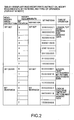
- FIG. 2 shows a TABLE 1 that lists exemplary read-modify-write instructions, modify requirements, bit patterns, and types of arithmetic operation (in case of 8-bit memory).
- the above exemplary modify requirements include the location of a bit. Instead of that, a bit pattern may directly be supplied to the RMWU 10, which however requires that the CPU 1 incorporates a bit-pattern generator.
- bit manipulation instructions are logical operation instructions performing between a memory operand and an immediate operand.
- modify requirements consist of the immediate operand and type of logical operation.
- a bit pattern for such processors is an immediate operand itself, hence no bit-pattern generators being required for the RMWU 10 or CPU 1.
- the RMWU 10 sends write data from the CPU 1 to the BIU 3 via the memory-write data buffer 17, and instructs the BIU 3 to start the write bus cycle.
- the BIU 3 then starts the write bus cycle to write the write data in the memory 2.
- the RMWU 10 instructs the BIU 3 to start the read bus cycle.
- the BIU 3 then starts the read bus cycle to read data from the memory 2.
- the read data is retuned to the RMWU 10 and then to the CPU 1 with no modifications.
- modify data and operation control signal in option (3) may be of modify data of "0" at every bit and a logical-OR operation control signal or modify data of "1" at every bit and a logical-AND operation control signal.
- the system shown in FIG. 1 employs the option (3).
- the RMWU 10 instructs the BIU 3 to start the read bus cycle.
- the BIU 3 then starts the read bus cycle to read data from the memory 2 and return it to the RMWU 10 as read data.
- the modify-requirements decoder 13 of the RMWU 10 generates modify data and an operation control signal from modify requirements.
- the modify operation circuit 15 applies an operation processing to the read data with the modify data under the operation control signal, the RMWU 10 returns the operation result to the CPU 1.
- FIG. 3 also shows a TABLE 2 that lists exemplary read-modify-write instructions, modify requirements, bit patterns, and types of arithmetic operation (for 8-bit memory).
- An operation result obtained under TABLE 2 in FIG. 3 may be returned to the CPU 1 as it is. Or, it may be tested whether all bits of the operation result "0", and "0" is retuned to the CPU 1 if the test shows positive whereas "1" returned if at least one bit is "1".
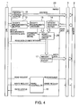
- FIG. 4 shows a processor according to a second embodiment of the present invention, a modification to the first embodiment.
- the feature of the second embodiment is that write data and a piece of information of modify requirements from a CPU 1 are transferred to a RMWU 20 through the same (common) signal lines.
- This feature is appropriate for a situation in that the CPU 1 has not simultaneously issued a read-modify-write instruction and a write instruction, and hence the RMWU 20 does not require modify data and write data at the same time.
- the modify data and the write data are sent from the CPU 1 to the RMWU 20 with using the common signal lines.
- Operation commands in modify requirements sending from the CPU 1 have a write command for the write instructions. If the operation command is the write command, a modify requirements buffer 12 of the RMWU 20 gets the data sending on the common signal lines as the write data; otherwise it gets the data as the modify data.
- the RMWU 20 does not instruct the BIU 3 to start the read bus cycle, an input (from a memory read data buffer 14) of the modify operation circuit 25 is neglected, the write data on the modify requirements buffer 12 is sent (1) directly to a memory write data buffer 17, or (2) via the modify operation circuit 25 without any modification, and then the write data on the memory write data buffer 17 is sent to the BIU 3.
- the RMWU 20 is provided with a memory address buffer 11 for storing memory addresses supplied by the CPU 1 and outputting them to the BIU 3; a modify-requirements buffer 12 for storing modify requirements which consist of the operation command and the data (the modify data for read-modify-write instructions or the write data for write instructions) supplied by the CPU 1; a modify-requirements decoder 13 for decoding the modify requirements to generate modify data/write data and the operation control signal; a memory read-data buffer 14 for storing read data; a modify operation circuit 25 for performing between the read data from the buffer 14 and the modify data/write data from the decoder 13 under the operation control signals from the decoder 13 to output the read data, the write data or modified data; the memory write-data buffer 17 for storing the read data or modified data from the operation circuit 25 as write data or the write data from the circuit 25 or from directly the decoder 13 and then outputting the stored write data to the BIU 3; and a RMWU controller 18 for outputting a read request or a
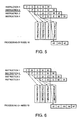
- FIG. 5 Disclosed first with reference to FIG. 5 is data processing with a processor in the third embodiment according to the present invention.
- FIG. 5 illustrates pipeline processing of 5-stage CPU 1 instructions of instruction fetch “F”, instruction decode “D”, computation execute “E”, memory access (or RMWU access) "M” and register write “W”. Each stage requires one machine cycle.
- the processor in the third embodiment disclosed below is a RISC type. Or, it may be a CISC type.
- INSTRUCTION 2 is a read-modify-write instruction.
- the memory access "M” includes memory read “rd”, data modify “mo” and memory write “wr” when the RMWU 10 in the first embodiment is employed.
- the read-modify-write instruction is executed by the CPU 1 under pipeline processing.
- the RMWU 10 receives a memory address and modify requirements from the CPU 1.
- the CPU 1 completes the memory-access stage in one machine cycle and moves onto the next register-write stage while the instruction following the read-modify-write instruction appears at the memory-access stage.
- the RMWU 10 sends a request of read bus cycle to the BIU 3.
- the request is held at the BIU 3 while the BIU 3 is using the bus for the preceding instruction.
- the read bus cycle starts when the bus is released from the preceding instruction. It can start immediately when the bus has been free.
- the BIU 3 starts to read the memory 2 at the memory address received from the RMWU 10.
- the BIU 3 sends the data read from the memory 2 to the RMWU 10.
- the BIU 3 suspends another unit's bus-cycle request until the RMWU 10 completes to write the modified data into the memory 2.
- the RMWU 10 modifies the read data under the modify requirements from the CPU 1 and instructs the BIU 3 to start a memory write bus cycle with the modified data as write data.
- Memory write is usually performed at the memory address already used in memory read.
- the BIU 3 writes the write data in the memory 2 and completes the read-modify-write operation.
- the CPU 1 is executing instructions following the read-modify-write instruction in pipeline processing while the RMWU 10 and the BIU 3 are proceeding with the read-modify-write operation.
- the read-modify-write instruction is thus executed as if it runs for one machine cycle in this pipeline processing.
- the present invention therefore achieves high-performance read-modify-write operation.
- FIG. 6 Disclosed next with reference to FIG. 6 is data processing with a processor in the fourth embodiment according to the present invention. Illustrated in FIG. 6 is execution of a read-modify-write instruction to a slow memory requiring access time of 2 machine cycles.
- INSTRUCTION 2 is a read-modify-write instruction.
- the instructions are instruction fetch “F”, instruction decode “D”, computation execute “E”, memory access (or RMWU access) "M” and register write “W”.
- the memory access (M) includes memory read “rd”, modify “mo” and memory write "wr” when the RMWU 10 in the first embodiment is employed, like shown in FIG. 5.
- a read bus cycle and a write bus cycle to be instructed to the BIU 3 from the CPU 1 require two machine cycles each. Nevertheless, the CPU 1 executes the succeeding instructions one by one in pipeline processing while the RMWU 10 is executing the read or write bus cycle.
- the CPU 1 executes the read-modify-write instruction in one machine cycle in pipeline processing to the memory 2 of a slow access time, according to the fourth embodiment.
- This high performance is very remarkable when compared to known processors with such a memory of a slow access time.
- the RMWU 10 with a FIFO (First-In-First-out) that stores memory addresses and modify requirements from the CPU 1 enables successive execution of read-modify-write instructions (several different instructions may be interposed) without stalling pipeline processing.
- the CPU 1 receives FIFO-busy/ready information as RMWU 10 status and, if the FIFO is busy, the CPU 1 stalls the pipeline processing of the read-modify-write instructions until the FIFO becomes ready.
- the RMWU 10 may instruct a write bus cycle to the BIU 3 for executing memory write instructions such as a store instruction.
- the present invention has enhanced a known write buffer unit (WBU) for only executing memory write instructions so that it can execute a sequence of memory read, modification and memory write, protect bus cycles from interruption and make adjustments between the sequence and instruction fetches and/or a memory-read bus cycle with the preceding memory-read instruction.
- WBU write buffer unit
- RMWU 10 capable of functions, such as a bit-test-and-set instruction, of modifying memory data (to set "1" at designated bits) while returning read data to the CPU 1.
- the RMWU 10 may return the read data to the CPU 1 as it is or modify it for testing before return. For example, when a read data is "10110010" and a bit position for testing and setting is 6, "10110010" is returned as it is, in the case where RMWU 10 returns a read data to the CPU 1 as it is.
- the RMWU 10 modifies the data for testing, the RMWU 10 performs a logical AND between the read data and "0100000" (an immediate value at which only bit 6 is set to 1) to return "00000000" or "0" having a content of which a location of bit 6 is 0.
- the CPU 1 writes the data returned from the RMWU 10 in a designated register at a register write stage, to complete the bit-test and -set instruction.
- the RMWU 10 or 20 in the present invention disclosed above is thus capable of executing a read-modify-write instruction in one machine cycle.
- the present invention therefore achieves high performance in processor-embedded equipment incorporating the RMWU 10 or 20.
- processors of fifth to seventh embodiments incorporating the RMWU 10 or 20, respectively, modifications to the third or the fourth embodiment.
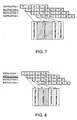
- Illustrated in FIG. 7 are operations of the processors in both of the fifth and the sixth embodiments.
- the processors execute a read-modify-write instruction of three operations (read, modify and write) at a memory access stage in 3 machine cycles while instructions following this instruction have been stalled before the memory access stage.
- the read-modify-write instruction in these embodiments requires 3 machine cycles for apparent execution time, thus almost no improvements in execution time in FIG. 7 compared to known processors.
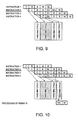
- the fifth and the sixth embodiments may not always necessary one machine cycle for a modify operation, as shown in FIGs. 8 and 9, respectively. This is because read-modify-write operations are performed at one memory access stage in these embodiments, with no pipeline-stage return, otherwise could require more than one machine cycle like the third known processor in FIG. 28.
- modify is performed with memory read at an Ms stage in the fifth embodiment shown in FIG. 8 or it is performed with memory write at an M stage in the sixth embodiment shown in FIG. 9.
- the fifth and the sixth embodiments therefore shorten the apparent execution time by 1 machine cycle from 3 to 2 machine cycles for INSTRUCTION 2.
- the modify operation with memory read at the Ms stage in the processor of the fifth embodiment requires a modify-data generator (modify-requirements decoder 13) and a modify operation circuit (15 or 25) like the RMWU 10 or 20 in the first or the second embodiment, between the CPU 1 and the BIU 3.
- read data from the BIU3 is modified in accordance with a modify requirements from the CPU 1.
- Read data is, however, returned to the CPU 1 with no modifications under a simple read instruction (i.e. a load instruction).
- INSTRUCTION 2 is the read-modify-write instruction with instruction fetch “F”, instruction decode “D”, computation execute “E”, stall "Ms” (read and modify executed at memory-access stage), memory access "M” and register write "W”.
- INSTRUCTIONS 3 and 4 have stall at instruction decode stage “Ds” and stall at execute stage “Es”, respectively.
- a modify-data generator modify-requirements decoder 13
- a modify operation circuit (15 or 25) are provided between the CPU 1 and the BIU 3, as the same manner of the RMWU 10 or 20 in the first or the second embodiment.
- write data from the CPU 1 is modified in accordance with modify requirements also from the CPU 1.
- Read data in a read bus cycle preceding a write bus cycle is returned to the CPU 1 without passing through the above modification circuitry in the sixth embodiment.
- INSTRUCTION 2 is the read-modify-write-instruction with an instruction fetch "F”, instruction decode “D”, computation execute "E”, stall at memory access stage “Ms” (read executed at memory-access stage), modify "Mm” and register write "W”.
- INSTRUCTIONS 3 and 4 have stall at execute stage “Es” and stall at instruction decode stage “Ds", respectively.
- the read-modify-write instruction is continuously stalled at the memory access stage "M". Nevertheless, the sixth embodiment shortens machine cycle by one compared to the known processors, because of no modifications.
- the processor of the sixth embodiment with a non-blocking load for executing succeeding instructions (not accessible to memory at stage "M") with no stalls in read cycle masks a waiting time for the read-modify-write instruction in read bus cycle for a memory of slow access time.
- the sixth embodiment achieves execution of instructions almost one-half the known processors in execution time.
- Illustrated in FIG. 10 is execution of instructions in the processor of the seventh embodiment.
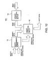
- the processor of the seventh embodiment is equipped with a modify write unit (abbreviated into MWU hereinafter) between the CPU 1 and the BIU 3.
- MWU corresponds to the RMWU 10 or 20 in the first or the second embodiment, respectively, but having no reading functions.
- the seventh embodiment performs reading from the memory and also writing to the MWU in two machine cycles at a memory-access stage, thus achieving higher processing speed than the known processors.
- stage "M" of a read-modify-write instruction is stalled until read is completed. On the contrary, it is not stalled while memory addresses and modify requirements are written into the FIFO of MWU if the FIFO is not full. It is, however, stalled when the FIFO is full.
- the seventh embodiment also achieves 2-machine-cycle instruction execution to memories of slow access time, with the non-blocking load described above to mask a waiting time caused by a read bus cycle.
- the first to the seventh embodiments achieve markedly high system performance with shortened execution time for read-modify-write instructions often used in embedded control system market.
- FIGs. 11 to 25 Disclosed next with reference to FIGs. 11 to 25 are eighth to twenty-first embodiments, respectively, according to the present invention, based on the foregoing embodiments.
- FIGs. 11 to 25 that are the same as or analogous to the elements shown in FIGs. 1 to 10 are referenced by the same reference numerals.
- the present invention provides processors with the built-in read-modify-write units to execute CPU instructions following the read-modify-write processing but in parallel with this processing.
- the present invention achieves high throughput and shortened apparent execution time for read-modify-write instructions.
Abstract
Description
- The present invention relates to a system having a read-modify-write instructions installed therein.
- Especially, this invention relates to a system having a read-modify-write unit for performing read-modify-write operations, in addition to a central processing unit (abbreviated into CPU hereinafter).
- Moreover, the present invention relates to a system having a read-modify-write unit and also a digital signal processing (abbreviated into DSP hereinafter) unit, applicable, not only to CPU, but to a digital signal processor, etc., for performing a series of read-modify-write operations, like a CPU.
- Microprocessors usually have a CPU incorporating an operation unit and a controller mounted on a silicon chip with LSI production technology. A computer system has such a microprocessor and memories connected thereto. Current microcomputers have memories also mounted on a microprocessor chip in which access is made between the microprocessor and memories via a bus interface unit (abbreviated into BIU hereinafter).
- Shown in FIG. 30 is known microprocessor architecture with a
CPU 1, amemory 2 and aBIU 3 interposed therebetween. - The
CPU 1 executes a read bus cycle, a write bus cycle or a dummy bus cycle (not read nor write) to thememory 2 via theBIU 3. In detail, the BIU 3 receives a memory address, a read or a write request and write data, data to be written (in writing only) from theCPU 1, while passes read data, data read from thememory 2 to theCPU 1. - FIG. 30 illustrates direct access to the
memory 2 by the BIU 3. Not only that, a memory controller (depending on the type of memory 2) may be provided between theBIU 3 and thememory 2, for read and write operations to the memory via the memory controller. - A read-modify-write instruction is explained in detail. This instruction is a single instruction for CPU to execute a series of operations to read data from a memory, modify some or all bits of the read data and then rewrite the original data with the modified data in the memory.
- The read-modify-write instruction is used, for example, for bit manipulation to 1-bit data, such as, bit set, bit clear, bit inversion and bit logical operations (LOGICAL ORAND, NOR, etc) and also for bit field manipulation to 2-bit data or more, such as, arithmetic operations, logical operations, shift/rotation, insertion/replacement and clear/set.
- Explained next is the bit manipulation and bit field manipulation to an 8-bit memory.
- In the following explanation, the most-significant bit and the least-significant bit are defined as
bit 7 andbit 0, respectively, for a binary-digit data "10101010" stored in the 8-bit memory at a given address. - The bit manipulation will be explained first for four cases.
- Bit set to
bit 2 replaces the value "0" ofbit 2 in "10101010" with "1", thus "10101110" being written in the 8-bit memory. - Bit clear to
bit 7 clears the value "1" ofbit 7 from "10101010" to have the value "0" forbit 7, thus "00101010" being written in the 8-bit memory. - Bit inversion to
bit 2 inverts the value "0" ofbit 2 to "1" in "10101010", thus "10101110" being written in the 8-bit memory. - Bit-LOGICAL OR operation to
bit 2 applies a logical OR between the value "1" and "0" ofbit 2 in "10101010" to have the result "1", thus "10101110" being written in the 8-bit memory. - Next, the bit field manipulation is explained for seven cases.
- Add operation to 3-bit data "010" of
bits 6 to 4 in "10101010" with the value "110" gives the value "000" as the lower three bits of the results (sum), that is, "010 + 110 = 1000", thus "10001010" being written in the 8-bit memory. - Subtract (or decrement) operation to 3-bit data "010" of
bits 6 to 4 in "10101010" from a value "1", that is, "010 - 1 = 001" results in "10011010" which is written in the 8-bit memory. - An EOR operation, an exclusive logical OR, with the value "110" to 3-bit data "010" of
bits 6 to 4 in "10101010" gives the value "100", thus "11001010" being written in the 8-bit memory. - Operational 1-bit right shift to 3-bit data "010" of
bits 6 to 4 in "10101010" gives the value "001", thus "10011010" being written in the 8-bit memory. - 1-bit right rotation to 4-bit data "0101" of
bits 6 to 3 in "10101010" rotates the value "0101" to the value "1010", thus "11010010" being written in the 8-bit memory. - Bit field insertion of the value "1101" to 4-bit data "0101" of
bits 6 to 3 in "10101010" replaces the value "1010" with "1101", thus "11101010" being written in the 8-bit memory. - Bit field clear to 4-bit data "0101" of
bits 6 to 3 in "10101010" results in "10000010" which is written in the 8-bit memory. - Execution of data read from a memory, data modify to the read data and data rewrite of the modified data to the memory with different instructions while interrupted by another task between these instructions could cause interruption before data modify or data rewrite to data to be rewritten. Such interruption could cause adverse consequences to system operations, such as, data look-up before data rewrite.
- To avoid such adverse consequences, a single read-modify-write instruction to execute read data, data modify and data write is required.
- The adverse consequences discussed above are, for example, as follows:
- Suppose that data for discriminating between a processing mode and a waiting mode are stored in a memory at certain addresses for two apparatus A and B, in which data "10" indicates that the apparatus A is in the processing mode, data "11" indicates that the apparatus B is in the processing mode and data "00" indicates that both of the apparatus A and B are in the waiting mode.
-
- The discriminating data is then read from the memory for the apparatus A to execute a specific processing. The data is rewritten as "10" if it is "00" and restored, thus the apparatus A starts the processing. On the contrary, if the data is not "00", the apparatus A waits until the data changes to "00". When the apparatus A completes the processing, the data "00" is written in the memory.
- Like the apparatus A, the apparatus B waits until the data changes to "00". The data "11" is then written so that the apparatus B can start a specific processing. The data "00" is also written when the apparatus B completes the processing.
- Read-modify-write processing is thus required for such a system in which the apparatus A and B are not allowed to simultaneously start processing so that processing will not be interrupt.
- When the read-modify-write processing is broken in while data read from the memory by the apparatus A has been "00", interruption occurs during data-"10" writing for the apparatus A to start processing. The interruption forces the apparatus B to read the data from the memory, thus the data "00" is read and hence the data "11" is written for the apparatus B to start processing instead of the apparatus A.
- When the interruption completes and the data "10" is written, the apparatus A starts processing even though the apparatus B is still in the processing mode.
- As discussed above, the apparatus A and B could suffer consequences in processing to be switched between the apparatus due to the interruption.
- The read-modify-write instruction includes bit manipulation, such as, bit set, bit clear, bit insertion, bit logical operations and bit inversion; bit field manipulation, such as, bit field insertion and bit field replacements; shift operations, such as, operation shift and logical shift; and add/subtract operations, such as, increment/decrement, as discussed above.
- Installation of the read-modify-write instruction in microprocessors, microcomputers and DSPs, etc., requires processing time over one machine cycle for each of instruction fetch, instruction decode, memory read, data modify and memory write.
- Illustrated in FIG. 26 is instruction execution in a first known CISC (Complex Instruction Set Computer) processor with no pipelined processing.
- A read-modify-write instruction (
INSTRUCTION 2 in FIG. 26) requires at least 5-machine-cycle instruction-execution time for instruction fetch "F", instruction decode "D", memory read "rd", data modify "mo", and memory write "wr". - Illustrated in FIG. 27 is instruction execution in a second known CISC processor with pipelined processing.
- Some instructions in a read-modify-write instruction can be executed in parallel with other preceding and succeeding instructions although it requires 5-machine-cycle instruction-execution time for instruction fetch "F", instruction decode "D", memory read "rd", data modify "mo" and memory write "wr".
- In detail, the F- and D-stages are executed while the preceding instructions "E" and "W" (INSTRUCTION 1) are being executed, and the mo- and wr-stages are executed while the succeeding instructions "F" and "D" (INSTRUCTION 3) are being executed. Therefore, the read-modify-write instruction is executed as if it runs for 3 machine cycles.
- FIG. 28 illustrates instruction execution in a third known RISC (Reduced Instruction Set Computer) processor with 5-stage pipelined processing.
- A pipeline has 5 stage of instruction fetch "F", instruction decode "D", computation execute "E", memory access "M" and register write "W".
- Two types of processing are performed at the memory-access "M" stage; memory read at the initial M stage; and memory write at the next M stage. Modify processing is performed when the pipeline processing returns to the instruction-decode "D" and computation-execute "E" stages.
- The pipeline processing is performed in the order of instruction fetch "F", instruction decode "D", computation execute "E", memory access "M" with memory read, instruction decode "D", computation execute "E" with data modify, memory access "M" with memory write and register write "W".
- While the pipeline processing is being returned, an instruction following the read-modify-write instruction is stalled before the pipeline processing enters into an instruction-decode stage. The read-modify-write instruction illustrated in FIG. 28 thus seems to have 4 machine cycles. The third known processor consumes 2 stages for data modify in returning pipeline processing.
- FIG. 29 illustrates read-modify-write processing for a fourth known processor that corresponds to the third known processor (FIG. 28) but to a memory with relatively slow read-write processing (such as a memory requiring 2 machine cycles for each of read and write).
- The read-modify-write instruction illustrated in FIG. 29 requires 5 machine cycles because a memory-access "M" stage requires at least 2 machine cycles.
- The slower the read-write processing for a memory used, the larger the number of machine cycles to be used for execution of the read-modify-write instruction, that is, machine cycles for the read-modify-write instruction = machine cycles for memory read + machine cycles for data modify + machine cycles for instruction execution.
- As discussed above, the read-modify-write instructions in the known first to the fourth known processors are relatively slow instructions requiring at least 3 to 5 machine cycles.
- The read-modify-write instruction requires longer execution time for slower processing-speed memories.
- Read-modify-write instructions, such as bit manipulation, usually occupy 10% to 15% of programs installed in electrical household appliances, such as air conditioners and digital camcorders, and AV (Audio-Visual) equipment, such as CD players, DVD players, TVs and VCRs. Instructions of slow execution speed but often used will cause low processor performances.
- A Read-modify-write-controlled system disclosed in Japanese Unexamined Patent publication No. 11-184761 has read-modify-write functions. The read-modify-write processing is performed simultaneously or in parallel to several memory banks. This is different from the present invention in which CPU instructions are executed in parallel with the preceding read-modify-write processing for higher throughput.
- Recent program-implemented equipment have become complex in processing. Moreover, there are demands for higher processing speed and/or lower power consumption. Higher system performance, or smaller number of clocks per instruction (abbreviated into CPI hereinafter) for each CPU instruction is strongly desired.
- Pipeline processing has been advanced for smaller CPI to meet the demands, however, obstructed by read-modify-write instructions such as bit manipulation due to 3 machine cycles or more in CPI.
- Moreover, slow access-time memories affect CPI in read-modify-write operations. For, example, a 2 machine-cycle access-time memory requires 5 (= 2 + 2 + 1) machine cycles in CPI for read-modify-write instructions.
- As discussed above, the known processors have long apparent execution time for read-modify-write instructions. Program-implemented equipment using many read-modify-write instructions thus have longer apparent execution time which give adverse affects to performances, particularly, of CPU-embedded system.
- In order to overcome the problems discussed above, a purpose of the present invention is to provide a system with shorter apparent execution time for read-modify-write instructions.
- Another purpose of the present invention is to provide a system capable of executing a read-modify-write instruction in one machine cycle like other instructions.
- A data processing system according to the present invention includes: a central processing unit to decode and execute given instructions; a memory to store given data; a bus interface unit, provided between the central processing unit and the memory, to start a read bus cycle to read data from the memory, a write bus cycle to write data to the memory, or a dummy bus cycle (different from the read and write bus cycles); and a read-modify-write unit provided between the central processing unit and the bus interface unit. The read-modify-write unit has: a modify- requirements buffer to store modify requirements composed of modify data output from the central processing unit and an operation control signal; and a modify operation circuit to apply an operation processing to read data output from the bus interface unit with the modify data output from the modify-requirements buffer under the operation control signal to output an operation result to the bus interface unit, as write data.
- In the drawings:
- FIG. 1 is a system block diagram incorporating a read-modify-write unit according to a first embodiment of the present invention;
- FIG. 2 is a table illustrating read-modify-write instructions used in the first embodiment;
- FIG. 3 is another table illustrating read-modify-write instructions used in the first embodiment;
- FIG. 4 is a system block diagram incorporating a read-modify-write unit according to a second embodiment of the present invention;
- FIG. 5 is an illustration indicating exemplary execution of read-modify-write instructions in a processor according to a third embodiment of the present invention;
- FIG. 6 is an illustration indicating exemplary execution of read-modify-write instructions in a processor according to a fourth embodiment of the present invention;
- FIG. 7 is an illustration indicating exemplary execution of read-modify-write instructions to be enhanced in processors according to fifth and sixth embodiments of the present invention;
- FIG. 8 is an illustration indicating exemplary execution of read-modify-write instructions enhanced in the processor according to the fifth embodiment of the present invention;
- FIG. 9 is an illustration indicating exemplary execution of read-modify-write instructions enhanced in the processor according to the sixth embodiment of the present invention;
- FIG. 10 is an illustration indicating exemplary execution of read-modify-write instructions in a processor according to a seventh embodiment of the present invention;
- FIG. 11 is a system block diagram incorporating a read-modify-write unit shared by eighth to twenty-first embodiments of the present invention;
- FIG. 12 is a system block diagram incorporating a read-modify-write unit according to the eighth embodiment of the present invention;
- FIG. 13 is a system block diagram incorporating a read-modify-write unit according to the ninth embodiment of the present invention;
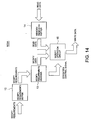
- FIG. 14 is a system block diagram incorporating a read-modify-write unit according to the tenth embodiment of the present invention;
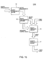
- FIG. 15 is a system block diagram incorporating a read-modify-write unit according to a first architecture in the eleventh embodiment of the present invention;
- FIG. 16 is a system block diagram incorporating a read-modify-write unit according to a second architecture in the twelfth embodiment of the present invention;
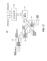
- FIG. 17 is a system block diagram incorporating a read-modify-write unit according to the thirteenth embodiment of the present invention;
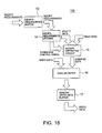
- FIG. 18 is a system block diagram incorporating a read-modify-write unit according to the fourteenth embodiment of the present invention;
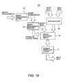
- FIG. 19 is a system block diagram incorporating a read-modify-write unit according to the fifteenth embodiment of the present invention;
- FIG. 20 is a system block diagram incorporating a read-modify-write unit according to the sixteenth embodiment of the present invention;
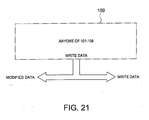
- FIG. 21 is a system block diagram incorporating a read-modify-write unit according to the seventeenth embodiment of the present invention;
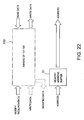
- FIG. 22 is a system block diagram incorporating a read-modify-write unit according to the eighteenth embodiment of the present invention;
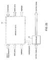
- FIG. 23 is a system block diagram incorporating a read-modify-write unit according to the nineteenth embodiment of the present invention;
- FIG. 24 is a system block diagram incorporating a read-modify-write unit according to the twentieth embodiment of the present invention;
- FIG. 25 is a system block diagram incorporating a read-modify-write unit according to the twenty-first embodiment of the present invention;
- FIG. 26 is an illustration showing a first known RMW processing in a CISC processor with no pipeline instruction execution;
- FIG. 27 is an illustration showing a second known RMW processing in a CISC processor with pipeline instruction execution;
- FIG. 28 is an illustration showing a third known RMW processing in a RISC processor with pipeline instruction execution;
- FIG. 29 is an illustration showing a fourth known RMW processing in the case of read/write processing to a memory having a slow access time, in a RISC processor with pipeline instruction execution; and
- FIG. 30 is a block diagram of a known processor having read-modify-write instructions.
-
- Embodiments of systems according to the present invention will be disclosed in detail with reference to the attached drawings.
- Disclosed first are a system architecture and its operational principle according to a first embodiment of the present invention with reference to FIGs. 1 to 3. The architecture of a processor according to a second embodiment, a modification to the first embodiment, will be disclosed next with reference to FIG. 4. Thereafter, the features of the present invention will be explained in accordance with several embodiments.
- Disclosed now with respect to FIG. 1 is the system architecture according to the first embodiment of the present invention.
- As shown in FIG. 1, the system according to the first embodiment at least includes a
CPU 1 for decoding and executing several instructions; amemory 2 for storing given data; and a bus interface unit (abbreviated into BIU hereinafter) 3, interposed between theCPU 1 and thememory 2, for starting a read bus cycle to read data from the memory if an address from theCPU 1 is within address space of thememory 2, a write bus cycle to write data to thememory 2 if an address from theCPU 1 is within address space of the memory, or a dummy bus cycle different from the read and write bus cycles. TheCPU 1, thememory 2 and theBIU 3 are analogous to those of the known system shown in FIG. 30. - A characteristic structure of the system in this embodiment is a read-modify-write unit (abbreviated into RMWU hereinafter) 10 for performing a memory-read processing, a data-modify processing and a memory-write processing under a read-modify-write (abbreviated into RMW occasionally) instruction.
- The detailed architecture of the
RMWU 10 will be disclosed with reference to FIG. 1. - The RMWU 10 is provided with a memory address buffer 11 for storing memory addresses supplied by the CPU 1 and outputting them to the BIU 3; a modify-requirements buffer 12 for storing modify requirements supplied by the CPU 1; a modify-requirements decoder 13 for decoding the modify requirements to generate modify data and an operation control signal; a memory read-data buffer 14 for storing read data (read from the memory 2) supplied by the BIU 3; a modify operation circuit 15 for applying an operation processing to the read data from the memory read-data buffer 14 with the modify data under the operation control signal to output the read data or modified data; a memory write-data buffer 17 for storing write data supplied by the CPU 1; a selector 16 for selecting either the write data from the write-data buffer 17 or the read data or the modified data from the modify operation circuit 15 and outputting the selected data to the BIU 3 as write data; and a RMWU controller 18 for receiving a read request, a write request or a read-modify-write request from the CPU 1 and outputting a control signal for requesting the read bus cycle, the write bus cycle or the dummy bus cycle to the BIU 3 so that a series of processing from read to write will not be interrupted when the read-modify-write request is sent from the CPU 1 and further outputting a busy-detection signal, to the CPU 1, indicating whether the RMWU 10 can accept another read request, write request or read-modify-write request from the CPU 1.
- In FIG. 1 (like FIG. 4 herein under), the read-modify-write request is not shown as an input of the
RMWU controller 18 because the modify requirements have the distinction of the write instruction and the read-modify-write instruction. Furthermore, if theCPU 1 causes only a read request to be active in the execution of a read instruction, only a write request to be active in the execution of a write instruction, and both the read request and the write request to be active in the execution of the read-modify-write instruction, it is unnecessary for theRMWU controller 18 to have the read-modify-write request as an input. Accordingly, in FIG. 1 (FIG. 4), the read-modify-write request is not shown as an input of theRMWU controller 18. - Disclosed next is the
RMWU 10 for its operation. - Supplied to the
RMWU 10 from theCPU 1 are a memory address, modify requirements, a read request, a write request, a read-modify-write request, write data, etc. - In response to the modify requirements and the read/write/read-modify-write requests, the
RMWU 10 sends the read bus cycle, the write bus cycle or the dummy bus cycle instruction to theBIU 3 for read-modify-write, data write or data read at the memory address. - In detail, the
RMWU 10 sends an instruction to theBIU 3 to start the read bus cycle in response to the read or the read-modify-write request. Read data is read from thememory 2, and it is supplied to theRMWU 10 via theBIU 3. The read data is sent to theCPU 1 directly or after modified at the modifyoperation circuit 15 of theRMWU 10, which depends on the type of a CPU instruction of which theCPU 1 requests to access thememory 2 via theRMWU 10. - For read-modify-write processing, the
RMWU 10 instructs theBIU 3 to start the read bus cycle. Then, theBIU 3 starts the read bus cycle, reads data from thememory 2 and sends the read data to theRMWU 10. - The modify-
requirements decoder 13 of theRMWU 10 generates modify data and an operation control signal in accordance with the modify requirements. The modifyoperation circuit 15 performs an operation according to the operation control signals between the read data and the modify data. - The operation result is sent to the
BIU 13 via theselector 16. TheRMWU 10 instructs theBIU 13 to start the bus write cycle. Thus, theRMWU 10 performs read-modify-write processing on behalf of theCPU 1. - Modify requirements consist of two pieces of information, such as, the location of a bit to be set and a bit set command, when the read-modify-write instruction is a bit set instruction.
- Based on the location of a bit to be set, the modify-
requirements decoder 13 of theRMWU 10 generates a bit pattern of "1" for the location of a bit to be set and "0" for the remaining bits. Thedecoder 13 further decodes the bit-set instruction to generate an operation control signal indicating a logical-OR operation. - The modify
operation circuit 15 performs a logical OR between the read data from theBIU 3 and the bit pattern. The operation result is sent to theBIU 3 as write data via theselector 16. TheRMWU 10 instructs theBIU 3 to start the write bus cycle for writing the write data to thememory 2. The memory address for the write data is usually the address used in a preceding memory read. - FIG. 2 shows a TABLE 1 that lists exemplary read-modify-write instructions, modify requirements, bit patterns, and types of arithmetic operation (in case of 8-bit memory).
- The above exemplary modify requirements include the location of a bit. Instead of that, a bit pattern may directly be supplied to the
RMWU 10, which however requires that theCPU 1 incorporates a bit-pattern generator. - There are processors in which bit manipulation instructions are logical operation instructions performing between a memory operand and an immediate operand. For such processors, modify requirements consist of the immediate operand and type of logical operation. A bit pattern for such processors is an immediate operand itself, hence no bit-pattern generators being required for the
RMWU 10 orCPU 1. - For write processing, the
RMWU 10 sends write data from theCPU 1 to theBIU 3 via the memory-write data buffer 17, and instructs theBIU 3 to start the write bus cycle. TheBIU 3 then starts the write bus cycle to write the write data in thememory 2. - For read processing, the
RMWU 10 instructs theBIU 3 to start the read bus cycle. TheBIU 3 then starts the read bus cycle to read data from thememory 2. The read data is retuned to theRMWU 10 and then to theCPU 1 with no modifications. - There are several ways of read-data return with no modifications, as follows:
- (1) read data is returned to the
CPU 1 not via theRMWU 10 but directly from theBIU 3; - (2) read data is returned to the
CPU 1 not via the modifyoperation circuit 15 but via the memory-readdata buffer 14; and - (3) modify data and an operation control signal, which will
give an operation result identical to read data, are generated
at the modify-
requirements decoder 13 and then the operation result is returned to theCPU 1 from the modifyoperation circuit 15. -
- The combination of modify data and operation control signal in option (3) may be of modify data of "0" at every bit and a logical-OR operation control signal or modify data of "1" at every bit and a logical-AND operation control signal. The system shown in FIG. 1 employs the option (3).
- There are instructions preinstalled in the
CPU 1, such as a bit test instruction, for modifying read data from thememory 2 and returning the modified data to theCPU 1 without writing the modified data in thememory 2. - In this case, the
RMWU 10 instructs theBIU 3 to start the read bus cycle. TheBIU 3 then starts the read bus cycle to read data from thememory 2 and return it to theRMWU 10 as read data. - The modify-
requirements decoder 13 of theRMWU 10 generates modify data and an operation control signal from modify requirements. The modifyoperation circuit 15 applies an operation processing to the read data with the modify data under the operation control signal, theRMWU 10 returns the operation result to theCPU 1. - FIG. 3 also shows a TABLE 2 that lists exemplary read-modify-write instructions, modify requirements, bit patterns, and types of arithmetic operation (for 8-bit memory). An operation result obtained under TABLE 2 in FIG. 3 may be returned to the
CPU 1 as it is. Or, it may be tested whether all bits of the operation result "0", and "0" is retuned to theCPU 1 if the test shows positive whereas "1" returned if at least one bit is "1". - FIG. 4 shows a processor according to a second embodiment of the present invention, a modification to the first embodiment.
- The feature of the second embodiment is that write data and a piece of information of modify requirements from a
CPU 1 are transferred to a RMWU 20 through the same (common) signal lines. - This feature is appropriate for a situation in that the
CPU 1 has not simultaneously issued a read-modify-write instruction and a write instruction, and hence theRMWU 20 does not require modify data and write data at the same time. - The modify data and the write data are sent from the
CPU 1 to theRMWU 20 with using the common signal lines. Operation commands in modify requirements sending from theCPU 1 have a write command for the write instructions. If the operation command is the write command, a modify requirements buffer 12 of theRMWU 20 gets the data sending on the common signal lines as the write data; otherwise it gets the data as the modify data. In the case of the write command, theRMWU 20 does not instruct theBIU 3 to start the read bus cycle, an input (from a memory read data buffer 14) of the modifyoperation circuit 25 is neglected, the write data on the modify requirements buffer 12 is sent (1) directly to a memorywrite data buffer 17, or (2) via the modifyoperation circuit 25 without any modification, and then the write data on the memorywrite data buffer 17 is sent to theBIU 3. - The
RMWU 20 is provided with amemory address buffer 11 for storing memory addresses supplied by theCPU 1 and outputting them to theBIU 3; a modify-requirements buffer 12 for storing modify requirements which consist of the operation command and the data (the modify data for read-modify-write instructions or the write data for write instructions) supplied by theCPU 1; a modify-requirements decoder 13 for decoding the modify requirements to generate modify data/write data and the operation control signal; a memory read-data buffer 14 for storing read data; a modifyoperation circuit 25 for performing between the read data from thebuffer 14 and the modify data/write data from thedecoder 13 under the operation control signals from thedecoder 13 to output the read data, the write data or modified data; the memory write-data buffer 17 for storing the read data or modified data from theoperation circuit 25 as write data or the write data from thecircuit 25 or from directly thedecoder 13 and then outputting the stored write data to theBIU 3; and aRMWU controller 18 for outputting a read request or a write request from theCPU 1 to theBIU 3 also a RMWU status signal to theCPU 1, indicating the status of theRMWU 20. - The processors in the first and second embodiments shown in FIGS. 1 and 4, respectively, both perform several specific operations according to the present invention, with different architectures.
- The specific operations according to the present invention will be disclosed in detail in third to fifth embodiments in which the first or the second embodiment is employed in processor hardware.
- Disclosed first with reference to FIG. 5 is data processing with a processor in the third embodiment according to the present invention.
- FIG. 5 illustrates pipeline processing of 5-
stage CPU 1 instructions of instruction fetch "F", instruction decode "D", computation execute "E", memory access (or RMWU access) "M" and register write "W". Each stage requires one machine cycle. The processor in the third embodiment disclosed below is a RISC type. Or, it may be a CISC type. - In FIG. 5,
INSTRUCTION 2 is a read-modify-write instruction. The memory access "M" includes memory read "rd", data modify "mo" and memory write "wr" when theRMWU 10 in the first embodiment is employed. - The read-modify-write instruction is executed by the
CPU 1 under pipeline processing. When the processing reaches the memory-access "M" stage, theRMWU 10 receives a memory address and modify requirements from theCPU 1. - The
CPU 1 completes the memory-access stage in one machine cycle and moves onto the next register-write stage while the instruction following the read-modify-write instruction appears at the memory-access stage. - During these CPU processing, the
RMWU 10 sends a request of read bus cycle to theBIU 3. The request is held at theBIU 3 while theBIU 3 is using the bus for the preceding instruction. The read bus cycle starts when the bus is released from the preceding instruction. It can start immediately when the bus has been free. - The
BIU 3 starts to read thememory 2 at the memory address received from theRMWU 10. TheBIU 3 sends the data read from thememory 2 to theRMWU 10. TheBIU 3 suspends another unit's bus-cycle request until theRMWU 10 completes to write the modified data into thememory 2. - The
RMWU 10 modifies the read data under the modify requirements from theCPU 1 and instructs theBIU 3 to start a memory write bus cycle with the modified data as write data. Memory write is usually performed at the memory address already used in memory read. TheBIU 3 writes the write data in thememory 2 and completes the read-modify-write operation. - The
CPU 1 is executing instructions following the read-modify-write instruction in pipeline processing while theRMWU 10 and theBIU 3 are proceeding with the read-modify-write operation. The read-modify-write instruction is thus executed as if it runs for one machine cycle in this pipeline processing. The present invention therefore achieves high-performance read-modify-write operation. - Disclosed next with reference to FIG. 6 is data processing with a processor in the fourth embodiment according to the present invention. Illustrated in FIG. 6 is execution of a read-modify-write instruction to a slow memory requiring access time of 2 machine cycles.
- In FIG. 6,
INSTRUCTION 2 is a read-modify-write instruction. The instructions are instruction fetch "F", instruction decode "D", computation execute "E", memory access (or RMWU access) "M" and register write "W". The memory access (M) includes memory read "rd", modify "mo" and memory write "wr" when theRMWU 10 in the first embodiment is employed, like shown in FIG. 5. - A read bus cycle and a write bus cycle to be instructed to the
BIU 3 from theCPU 1 require two machine cycles each. Nevertheless, theCPU 1 executes the succeeding instructions one by one in pipeline processing while theRMWU 10 is executing the read or write bus cycle. - In other words, the
CPU 1 executes the read-modify-write instruction in one machine cycle in pipeline processing to thememory 2 of a slow access time, according to the fourth embodiment. This high performance is very remarkable when compared to known processors with such a memory of a slow access time. - The
RMWU 10 with a FIFO (First-In-First-out) that stores memory addresses and modify requirements from theCPU 1 enables successive execution of read-modify-write instructions (several different instructions may be interposed) without stalling pipeline processing. TheCPU 1 receives FIFO-busy/ready information as RMWU 10 status and, if the FIFO is busy, theCPU 1 stalls the pipeline processing of the read-modify-write instructions until the FIFO becomes ready. - Not only the read and write bus cycle, the
RMWU 10 may instruct a write bus cycle to theBIU 3 for executing memory write instructions such as a store instruction. - The present invention has enhanced a known write buffer unit (WBU) for only executing memory write instructions so that it can execute a sequence of memory read, modification and memory write, protect bus cycles from interruption and make adjustments between the sequence and instruction fetches and/or a memory-read bus cycle with the preceding memory-read instruction. These are also features of the present invention.
- Also proposed in the present invention is a RMWU 10 capable of functions, such as a bit-test-and-set instruction, of modifying memory data (to set "1" at designated bits) while returning read data to the
CPU 1. - On receiving read data from the
BIU 3, theRMWU 10 may return the read data to theCPU 1 as it is or modify it for testing before return. For example, when a read data is "10110010" and a bit position for testing and setting is 6, "10110010" is returned as it is, in the case whereRMWU 10 returns a read data to theCPU 1 as it is. On the other hand, in the case where theRMWU 10 modifies the data for testing, theRMWU 10 performs a logical AND between the read data and "0100000" (an immediate value at which only bit 6 is set to 1) to return "00000000" or "0" having a content of which a location ofbit 6 is 0. TheCPU 1 writes the data returned from the RMWU 10 in a designated register at a register write stage, to complete the bit-test and -set instruction. - The
RMWU RMWU - Disclosed next with respect to FIGs. 7 to 10 are processors of fifth to seventh embodiments incorporating the
RMWU - Illustrated in FIG. 7 are operations of the processors in both of the fifth and the sixth embodiments. The processors execute a read-modify-write instruction of three operations (read, modify and write) at a memory access stage in 3 machine cycles while instructions following this instruction have been stalled before the memory access stage.
- The read-modify-write instruction in these embodiments requires 3 machine cycles for apparent execution time, thus almost no improvements in execution time in FIG. 7 compared to known processors.
- Nevertheless, the fifth and the sixth embodiments may not always necessary one machine cycle for a modify operation, as shown in FIGs. 8 and 9, respectively. This is because read-modify-write operations are performed at one memory access stage in these embodiments, with no pipeline-stage return, otherwise could require more than one machine cycle like the third known processor in FIG. 28.
- In detail, modify is performed with memory read at an Ms stage in the fifth embodiment shown in FIG. 8 or it is performed with memory write at an M stage in the sixth embodiment shown in FIG. 9.
- The fifth and the sixth embodiments therefore shorten the apparent execution time by 1 machine cycle from 3 to 2 machine cycles for
INSTRUCTION 2. - The modify operation with memory read at the Ms stage in the processor of the fifth embodiment requires a modify-data generator (modify-requirements decoder 13) and a modify operation circuit (15 or 25) like the
RMWU CPU 1 and theBIU 3. - Under a read-modify-write instruction, read data from the BIU3 is modified in accordance with a modify requirements from the
CPU 1. Read data is, however, returned to theCPU 1 with no modifications under a simple read instruction (i.e. a load instruction). - In FIG. 8,
INSTRUCTION 2 is the read-modify-write instruction with instruction fetch "F", instruction decode "D", computation execute "E", stall "Ms" (read and modify executed at memory-access stage), memory access "M" and register write "W".INSTRUCTIONS - On the other hand, in the processor of the sixth embodiment as shown in FIG. 9, in case of the write operation, a modify-data generator (modify-requirements decoder 13) and a modify operation circuit (15 or 25) are provided between the
CPU 1 and theBIU 3, as the same manner of theRMWU CPU 1 is modified in accordance with modify requirements also from theCPU 1. Read data in a read bus cycle preceding a write bus cycle is returned to theCPU 1 without passing through the above modification circuitry in the sixth embodiment. - Illustrated in FIG. 9 is execution of instructions in the processor of the sixth embodiment.
INSTRUCTION 2 is the read-modify-write-instruction with an instruction fetch "F", instruction decode "D", computation execute "E", stall at memory access stage "Ms" (read executed at memory-access stage), modify "Mm" and register write "W".INSTRUCTIONS - In case of read-modify-write operation to a memory of slow access time, the read-modify-write instruction is continuously stalled at the memory access stage "M". Nevertheless, the sixth embodiment shortens machine cycle by one compared to the known processors, because of no modifications.
- Moreover, the processor of the sixth embodiment with a non-blocking load for executing succeeding instructions (not accessible to memory at stage "M") with no stalls in read cycle masks a waiting time for the read-modify-write instruction in read bus cycle for a memory of slow access time. Thus, the sixth embodiment achieves execution of instructions almost one-half the known processors in execution time.
- Illustrated in FIG. 10 is execution of instructions in the processor of the seventh embodiment.
- Although not shown, the processor of the seventh embodiment is equipped with a modify write unit (abbreviated into MWU hereinafter) between the
CPU 1 and theBIU 3. The MWU corresponds to theRMWU - The seventh embodiment performs reading from the memory and also writing to the MWU in two machine cycles at a memory-access stage, thus achieving higher processing speed than the known processors.
- For memories of slow access time, the stage "M" of a read-modify-write instruction is stalled until read is completed. On the contrary, it is not stalled while memory addresses and modify requirements are written into the FIFO of MWU if the FIFO is not full. It is, however, stalled when the FIFO is full.
- The seventh embodiment also achieves 2-machine-cycle instruction execution to memories of slow access time, with the non-blocking load described above to mask a waiting time caused by a read bus cycle.
- As disclosed above, the first to the seventh embodiments achieve markedly high system performance with shortened execution time for read-modify-write instructions often used in embedded control system market.
- Disclosed next with reference to FIGs. 11 to 25 are eighth to twenty-first embodiments, respectively, according to the present invention, based on the foregoing embodiments.
- Elements shown in FIGs. 11 to 25 that are the same as or analogous to the elements shown in FIGs. 1 to 10 are referenced by the same reference numerals.
- (1) As shown in FIGs. 11 and 12, a
system 30 having a read-modify-write unit 10A (101) according to the eighth embodiment of the present invention incorporates aCPU 1 for decoding and executing several instructions; amemory 2 for storing given data; and aBIU 3, interposed between theCPU 1 and thememory 2, for starting a read bus cycle, a write bus cycle or a dummy bus cycle different from the read and write bus cycles, to read data from or write data to thememory 2. Thesystem 30 is further provided, between theCPU 1 and theBIU 3, with a modify-requirements buffer 12 for storing modify requirements supplied by theCPU 1; a memory read-data buffer 14 for storing read data output from theBIU 3; a modifyoperation circuit 15 for applying an operation processing to the read data from thebuffer 14 with the modify data from thebuffer 12 under an operation control signal also from thebuffer 12 to output the resultant modified data to theBIU 3, as write data. - (2) As shown in FIGs. 11 and 13, a
system 30 having a read-modify-write unit 10A (102) according to the ninth embodiment of the present invention incorporates aCPU 1 for decoding and executing several instructions; amemory 2 for storing given data; and aBIU 3, interposed between theCPU 1 and thememory 2, for starting a read bus cycle, a write bus cycle or a dummy bus cycle different from the read and write bus cycles, to read data from or write data to thememory 2. Thesystem 30 is further provided, between theCPU 1 and theBIU 3, with a modify-requirements buffer 12 for storing modify requirements supplied by theCPU 1; a modifyoperation circuit 15 for applying an operation processing to the read data output from theBIU 3 with the modify data from thebuffer 12 under an operation control signal from thebuffer 12; and a memory write-data buffer 17 for storing modified data from theoperation circuit 15, as write data, and outputting the data to theBIU 3. - (3) As shown in FIG. 11 and also FIG. 14 or 15, a
system 30 having a read-modify-write unit requirements decoder 13 between a modify-requirements buffer 12 for storing modify requirements output from the CPU 1 (in which the modify requirements are obtained by encoding the modify data and the operation control signal) and the modifyoperation circuit 15. The modifyrequirements decoder 13 decodes the modify requirements into modify data and an operation control signal. - (4) As shown in FIGs. 11 and 16, a system according to the
twelfth embodiment of the present invention, based on the system
(1) or (3), may have a memory write-
data buffer 12 for storing write data from theCPU 1 and adata selector 16 for selecting either the write data from thebuffer 12 or the modified data from the modifyoperation circuit 15. - (5) As shown in FIGs. 11 and 17, a system according to the
thirteenth embodiment of the present invention, based on the system
(1) or (3), may have, instead of the memory read-
data buffer 14, adata selector 16 for selecting either the write data from theCPU 1 or the read data read from thememory 2 via theBIU 3 and adata buffer 14 for storing the selected data from theselector 16 and supplying the stored data in thedata buffer 14 to the modifyoperation circuit 15. - (6) As shown in FIGs. 11 and 18, a system according to the
fourteenth embodiment of the present invention, based on the system
(2) or (3), may have a
data selector 16 for selecting either the write data from theCPU 1 or the modified data from the modifyoperation circuit 15 and outputting the selected data to the memory write-data buffer 17. - (7) As shown in any combination of FIGs. 11 and 13, FIGs.
11 and 14, FIGs. 11 and 15, or FIGs. 11 and 19, a system according
to the fifteenth embodiment of the present invention, based on
the system (2) or (3), may have a
data selector 16 for selecting either the write data from theCPU 1 or the read data read from thememory 2 via theBIU 3 and outputting the selected data to the modifyoperation circuit 15. - (8) As shown in FIGs. 11 and 20, a system according to the
sixteenth embodiment of the present invention, based on the system
(1), (2) or (3), may have a
data selector 16 for selecting either the write data from theCPU 1 or the modify data from the modify-requirements buffer 12 and outputting the selected data to the modifyoperation circuit 15. - (9) As shown in FIGs. 11 to 21, a system according to the
seventeenth embodiment of the present invention, based on any
one of the systems (1) to (8), may have an function of outputting
the modified data from the modify
operation circuit 15 to theCPU 1. - (10) As shown in FIGs. 11 to 22, a system according to the
eighteenth embodiment of the present invention, based on any one
of the systems (1) to (9), may have a
memory address buffer 31 for storing the memory addresses from theCPU 1 and outputting them to theBIU 3. - (11) As shown in FIGs. 11 to 23, a system according to the
nineteenth embodiment of the present invention, based on any one
of the systems (1) to (10), may have a
controller 32 for receiving the read request, the write request or the read-modify-write request from theCPU 1 and, on receiving the read-modify-write request, outputting a control signal carrying a read, a write or a dummy bus cycle to theBIU 3. Thecontroller 32 controls a series of processing from a read bus cycle to a write bus cycle without an interruption during a read-modify-write request. - (12) As shown in FIGs. 11 to 24, a system according to the
twentieth embodiment of the present invention, based the system
(11), the
controller 32 may have adetector 33 for detecting a busy state in which thecontroller 32 cannot accept any one of new read, write and read-modify-write requests from theCPU 1 and outputting a detected result (a busy detection signal) to theCPU 1. - (13) As shown in FIGs. 11 to 25, a system according to the
twenty-first embodiment of the present invention, based on any
one of the systems (1) to (12), may have a function of outputting
the read data from the
BIU 3 to theCPU 1. -
- As disclosed in detail, the present invention provides processors with the built-in read-modify-write units to execute CPU instructions following the read-modify-write processing but in parallel with this processing.
- Therefore, the present invention achieves high throughput and shortened apparent execution time for read-modify-write instructions.
- Especially, based on the basic idea in the present invention, it is possible to execute each read-modify-write instruction in one machine cycle like other instructions.
Claims (24)
- A data processing system comprising:a central processing unit to decode and execute given instructions;a memory to store given data;a bus interface unit, provided between the central processing unit and the memory, to start a read bus cycle to read data from the memory, a write bus cycle to write data to the memory, or a dummy bus cycle different from the read and write bus cycles; anda read-modify-write unit provided between the central processing unit and the bus interface unit, the read-modify-write unit including:a modify-requirements buffer to store modify requirements composed of modify data output from the central processing unit and an operation control signal; anda modify operation circuit to apply an operation processing to read data output from the bus interface unit with the modify data output from the modify-requirements buffer under the operation control signal to output an operation result to the bus interface unit, as write data.
- The data processing system according to claim 1, wherein the read-modify-write unit further includes a memory read-data buffer to store the read data output from the bus interface unit, the modify operation circuit applying the operation processing to the read data output from the memory read-data buffer with the modify data from the modify-requirements buffer.
- The data processing system according to claim 2, wherein the central processing unit outputs modify requirements obtained by encoding the modify data and the operation control signal, the read-modify-write unit further including a modify-requirements decoder, provided between the modify-requirements buffer for storing the output modify requirements and the modify operation circuit, to decode the output modify requirements into modify data and an operation control signal.
- The data processing system according to claim 2, wherein the read-modify-write unit further includes:a memory write-data buffer to store write data supplied by the central processing unit; anda selector to select either the write data output from the memory write-data buffer or modified data that is the operation result output from the modify operation circuit and output the selected data to the bus interface unit.
- The data processing system according to claim 4, wherein the modified data output from the modify operation circuit of the read-modify-write unit is output to the central processing unit.
- The data processing system according to claim 2, wherein the read-modify-write unit further includes:a data selector to select either write data supplied by the central processing unit or read data read from the memory via the bus interface unit; anda data buffer to store data output from the data selector and supply the stored data to the modify operation circuit.
- The data processing system according to claim 2, wherein the read-modify-write unit further includes a data selector to select either write data supplied by the central processing unit or modify data output from the modify-requirements buffer and output the selected data to the modify operation circuit.
- The data processing system according to claim 2, wherein the read-modify-write unit further includes a memory address buffer to store a memory address output from the central processing unit and output the stored memory address to the bus interface unit.
- The data processing system according to claim 2, wherein the read-modify-write unit further includes a controller to receive a read request, a write request or a read-modify-write request output from the central processing unit and output a control signal for requesting the read bus cycle, the write bus cycle or the dummy bus cycle to the bus interface unit, in response to the read-modify-write request, to avoid interruption in a series of processing from read to write.
- The data processing system according to claim 9, wherein the controller has a detector to detect a busy state in which the controller cannot accept any one of new read, write and read-modify-write requests from the central processing unit and output a busy detection signal carrying a detected result.
- The data processing system according to claim 10, wherein the read data output from the bus interface unit is output to the central processing unit.
- The data processing system according to claim 1, wherein the modify operation circuit applies the operation processing between the read data read from the memory via the bus interface unit and the modify data output from the modify-requirements buffer under the operation control signal also output from the modify-requirements buffer, the read-modify-write unit further including a memory write-data buffer to store write data that is the operation result output from the modify operation circuit and output the write data to the bus interface unit.
- The data processing system according to claim 12, wherein the central processing unit outputs modify requirements obtained by encoding the modify data and the operation control signal, the read-modify-write unit further including a modify-requirements decoder, provided between the modify-requirements buffer for storing the output modify requirements and the modify operation circuit, the modify-requirements decoder decoding the output modify requirement into modify data and an operation control signal.
- The data processing system according to claim 13, wherein the read-modify-write unit further includes:a memory write-data buffer to store write data supplied by the central processing unit; anda selector to select either the write data output from the memory write-data buffer or modified data that is the operation result output from the modify operation circuit, the selected data being output to the bus interface unit as write data.
- The data processing system according to claim 14, wherein the modified data output from the modify operation circuit of the read-modify-write unit is output to the central processing unit.
- The data processing system according to claim 13, wherein the read-modify-write unit further includes:a data selector to select either write data supplied by the central processing unit or read data read from the memory via the bus interface unit; anda data buffer to store data output from the data selector and supply the stored data to the modify operation circuit.
- The data processing system according to claim 12, wherein the read-modify-write unit further includes a data selector to select either write data supplied by the central processing unit or modified data output from the modify operation circuit and output the selected data to the memory write-data buffer.
- The data processing system according to claim 12, wherein the read-modify-write unit further includes a data selector to select either write data supplied by the central processing unit or read data read from the memory via the bus interface unit and output the selected data to the modify operation circuit.
- The data processing system according to claim 12, wherein the read-modify-write unit further includes a data selector to select either write data supplied by the central processing unit or modify data output from the modify-requirements buffer and output the selected data to the modify operation circuit.
- The data processing system according to claim 12, wherein the read-modify-write unit further includes a memory address buffer to store a memory address output from the central processing unit and output the stored memory address to the bus interface unit.
- The data processing system according to claim 12, wherein the read-modify-write unit further includes a controller to receive a read request, a write request or a read-modify-write request output from the central processing unit and output a control signal for requesting the read bus cycle, the write bus cycle or the dummy bus cycle to the bus interface unit, in response to the read-modify-write request, to avoid interruption in a series of processing from read to write.
- The data processing system according to claim 21, wherein the controller has a detector to detect a busy state in which the controller cannot accept any one of new read, write and read-modify-write requests from the central processing unit and output a busy detection signal carrying a detected result.
- The data processing system according to claim 22, wherein the read data output from the bus interface unit is output to the central processing unit.
- The data processing system according to claim 1, wherein the read-modify-write unit further includes:wherein the modify operation circuit performs the operation processing between the read data output from the memory read-data buffer and the modify data output from a modify requirements buffer under the operation control signal.a memory read-data buffer to store read data output from the bus interface unit; anda memory write-data buffer to store write data that is the operation result output from the modify operation circuit and output the stored data to the bus interface unit,
Applications Claiming Priority (2)
| Application Number | Priority Date | Filing Date | Title |
|---|---|---|---|
| JP2001391671A JP2003196084A (en) | 2001-12-25 | 2001-12-25 | System having read modifying write unit |
| JP2001391671 | 2001-12-25 |
Publications (3)
| Publication Number | Publication Date |
|---|---|
| EP1324190A2 true EP1324190A2 (en) | 2003-07-02 |
| EP1324190A3 EP1324190A3 (en) | 2004-08-11 |
| EP1324190B1 EP1324190B1 (en) | 2008-01-23 |
Family
ID=19188549
Family Applications (1)
| Application Number | Title | Priority Date | Filing Date |
|---|---|---|---|
| EP02028779A Expired - Lifetime EP1324190B1 (en) | 2001-12-25 | 2002-12-23 | Data processing system having a read-modify-write unit |
Country Status (5)
| Country | Link |
|---|---|
| US (1) | US6959367B2 (en) |
| EP (1) | EP1324190B1 (en) |
| JP (1) | JP2003196084A (en) |
| KR (1) | KR100533296B1 (en) |
| DE (1) | DE60224774T2 (en) |
Cited By (1)
| Publication number | Priority date | Publication date | Assignee | Title |
|---|---|---|---|---|
| WO2011022114A1 (en) | 2009-08-20 | 2011-02-24 | Rambus Inc. | Atomic memory device |
Families Citing this family (25)
| Publication number | Priority date | Publication date | Assignee | Title |
|---|---|---|---|---|
| US20050262403A1 (en) * | 2004-05-21 | 2005-11-24 | Alexandre Palus | Apparatus and method for single operation read-modify-write in a bit-accessible memory unit memory |
| US20060036817A1 (en) * | 2004-08-10 | 2006-02-16 | Oza Alpesh B | Method and system for supporting memory unaligned writes in a memory controller |
| US7627723B1 (en) * | 2006-09-21 | 2009-12-01 | Nvidia Corporation | Atomic memory operators in a parallel processor |
| US8239638B2 (en) | 2007-06-05 | 2012-08-07 | Apple Inc. | Store handling in a processor |
| US7836262B2 (en) | 2007-06-05 | 2010-11-16 | Apple Inc. | Converting victim writeback to a fill |
| JP2009032323A (en) * | 2007-07-26 | 2009-02-12 | Toshiba Corp | Disk storage device |
| US8135926B1 (en) * | 2008-10-21 | 2012-03-13 | Nvidia Corporation | Cache-based control of atomic operations in conjunction with an external ALU block |
| US8473695B2 (en) * | 2011-03-31 | 2013-06-25 | Mosys, Inc. | Memory system including variable write command scheduling |
| US9354823B2 (en) | 2012-06-06 | 2016-05-31 | Mosys, Inc. | Memory system including variable write burst and broadcast command scheduling |
| US8850137B2 (en) * | 2010-10-11 | 2014-09-30 | Cisco Technology, Inc. | Memory subsystem for counter-based and other applications |
| JP5480793B2 (en) * | 2010-12-10 | 2014-04-23 | 株式会社日立製作所 | Programmable controller |
| US8688957B2 (en) * | 2010-12-21 | 2014-04-01 | Intel Corporation | Mechanism for conflict detection using SIMD |
| KR101975534B1 (en) * | 2012-09-11 | 2019-05-07 | 삼성전자주식회사 | Semiconductor memory device with operation functions |
| US9411592B2 (en) | 2012-12-29 | 2016-08-09 | Intel Corporation | Vector address conflict resolution with vector population count functionality |
| US9411584B2 (en) | 2012-12-29 | 2016-08-09 | Intel Corporation | Methods, apparatus, instructions, and logic to provide vector address conflict detection functionality |
| CN104102584A (en) * | 2014-08-08 | 2014-10-15 | 珠海格力电器股份有限公司 | Air conditioning unit test method, test control device and test system |
| JP2017123208A (en) * | 2016-01-06 | 2017-07-13 | ルネサスエレクトロニクス株式会社 | Semiconductor storage device |
| US11188239B2 (en) | 2019-03-28 | 2021-11-30 | Western Digital Technologies, Inc. | Host-trusted module in data storage device |
| KR20200126155A (en) | 2019-04-29 | 2020-11-06 | 에스케이하이닉스 주식회사 | Semiconductor memory device performing command merging and operating method thereof |
| US11061820B2 (en) * | 2019-08-30 | 2021-07-13 | Microsoft Technology Licensing, Llc | Optimizing access to page table entries in processor-based devices |
| KR102456176B1 (en) | 2020-05-21 | 2022-10-19 | 에스케이하이닉스 주식회사 | Memory controller and operating method thereof |
| US11573891B2 (en) | 2019-11-25 | 2023-02-07 | SK Hynix Inc. | Memory controller for scheduling commands based on response for receiving write command, storage device including the memory controller, and operating method of the memory controller and the storage device |
| KR20210063724A (en) * | 2019-11-25 | 2021-06-02 | 에스케이하이닉스 주식회사 | Memory system |
| KR20210081663A (en) * | 2019-12-24 | 2021-07-02 | 삼성전자주식회사 | Interconnect device, operation method of interconnect device, and artificial intelligence(ai) accelerator system |
| US11630605B1 (en) * | 2022-08-10 | 2023-04-18 | Recogni Inc. | Methods and systems for processing read-modify-write requests |
Citations (1)
| Publication number | Priority date | Publication date | Assignee | Title |
|---|---|---|---|---|
| US5666515A (en) * | 1993-02-18 | 1997-09-09 | Unisys Corporation | Information processing system having multiple modules and a memory on a bus, where any module can lock an addressable portion of the memory by sending retry signals to other modules that try to read at the locked address |
Family Cites Families (9)
| Publication number | Priority date | Publication date | Assignee | Title |
|---|---|---|---|---|
| JP3038781B2 (en) | 1989-04-21 | 2000-05-08 | 日本電気株式会社 | Memory access control circuit |
| JPH0581122A (en) | 1991-09-20 | 1993-04-02 | Pfu Ltd | System for controlling partial write of memory |
| US5572702A (en) * | 1994-02-28 | 1996-11-05 | Intel Corporation | Method and apparatus for supporting read, write, and invalidation operations to memory which maintain cache consistency |
| JPH0954694A (en) | 1995-08-16 | 1997-02-25 | Nec Corp | Pipeline processor and its processing method |
| US6745302B1 (en) * | 1996-08-20 | 2004-06-01 | Sony Corporation | Method and circuit for enabling a clock-synchronized read-modify-write operation on a memory array |
| US6405276B1 (en) * | 1998-12-10 | 2002-06-11 | International Business Machines Corporation | Selectively flushing buffered transactions in a bus bridge |
| US6226017B1 (en) | 1999-07-30 | 2001-05-01 | Microsoft Corporation | Methods and apparatus for improving read/modify/write operations |
| JP2001075826A (en) | 1999-09-09 | 2001-03-23 | Hitachi Ltd | System for high-efficiency semaphore processing by parallel computer |
| US6795901B1 (en) * | 1999-12-17 | 2004-09-21 | Alliant Techsystems Inc. | Shared memory interface with conventional access and synchronization support |
-
2001
- 2001-12-25 JP JP2001391671A patent/JP2003196084A/en active Pending
-
2002
- 2002-12-23 DE DE60224774T patent/DE60224774T2/en not_active Expired - Lifetime
- 2002-12-23 EP EP02028779A patent/EP1324190B1/en not_active Expired - Lifetime
- 2002-12-23 US US10/325,935 patent/US6959367B2/en active Active
- 2002-12-24 KR KR10-2002-0083378A patent/KR100533296B1/en not_active IP Right Cessation
Patent Citations (1)
| Publication number | Priority date | Publication date | Assignee | Title |
|---|---|---|---|---|
| US5666515A (en) * | 1993-02-18 | 1997-09-09 | Unisys Corporation | Information processing system having multiple modules and a memory on a bus, where any module can lock an addressable portion of the memory by sending retry signals to other modules that try to read at the locked address |
Non-Patent Citations (2)
| Title |
|---|
| "RECHENLEISTUNG FUER DIE MOTORSTEURERUNG" ELEKTRONIK, FRANZIS VERLAG GMBH. MUNCHEN, DE, vol. 49, no. 9, 2 May 2000 (2000-05-02), page 16 XP001048957 ISSN: 0013-5658 * |
| FREEMAN C P: "READ-MODIFY-WRITE DATA INTEGRITY" IBM TECHNICAL DISCLOSURE BULLETIN, IBM CORP. NEW YORK, US, vol. 27, no. 8, 1985, pages 5019-5020, XP000714709 ISSN: 0018-8689 * |
Cited By (9)
| Publication number | Priority date | Publication date | Assignee | Title |
|---|---|---|---|---|
| WO2011022114A1 (en) | 2009-08-20 | 2011-02-24 | Rambus Inc. | Atomic memory device |
| EP2467852A1 (en) * | 2009-08-20 | 2012-06-27 | Rambus Inc. | Atomic memory device |
| EP2467852A4 (en) * | 2009-08-20 | 2014-04-02 | Rambus Inc | Atomic memory device |
| US9658953B2 (en) | 2009-08-20 | 2017-05-23 | Rambus Inc. | Single command, multiple column-operation memory device |
| US9898400B2 (en) | 2009-08-20 | 2018-02-20 | Rambus Inc. | Single command, multiple column-operation memory device |
| US10552310B2 (en) | 2009-08-20 | 2020-02-04 | Rambus Inc. | Single command, multiple column-operation memory device |
| US11204863B2 (en) | 2009-08-20 | 2021-12-21 | Rambus Inc. | Memory component that performs data write from pre-programmed register |
| US11720485B2 (en) | 2009-08-20 | 2023-08-08 | Rambus Inc. | DRAM with command-differentiated storage of internally and externally sourced data |
| US11748252B2 (en) | 2009-08-20 | 2023-09-05 | Rambus Inc. | Data write from pre-programmed register |
Also Published As
| Publication number | Publication date |
|---|---|
| EP1324190B1 (en) | 2008-01-23 |
| KR100533296B1 (en) | 2005-12-05 |
| EP1324190A3 (en) | 2004-08-11 |
| KR20030055148A (en) | 2003-07-02 |
| US6959367B2 (en) | 2005-10-25 |
| JP2003196084A (en) | 2003-07-11 |
| DE60224774D1 (en) | 2008-03-13 |
| DE60224774T2 (en) | 2009-01-15 |
| US20030120880A1 (en) | 2003-06-26 |
Similar Documents
| Publication | Publication Date | Title |
|---|---|---|
| US6959367B2 (en) | System having read-modify-write unit | |
| US6115808A (en) | Method and apparatus for performing predicate hazard detection | |
| JP5431308B2 (en) | Using local condition code registers to accelerate conditional instruction execution in systems and pipeline processors | |
| KR100335785B1 (en) | Execution of data processing instructions | |
| WO1983001133A1 (en) | Microprocessor with memory having interleaved address inputs and interleaved instruction and data outputs | |
| US7376820B2 (en) | Information processing unit, and exception processing method for specific application-purpose operation instruction | |
| JP2620511B2 (en) | Data processor | |
| JP2535252B2 (en) | Parallel processor | |
| KR20200088760A (en) | Checksum generation | |
| US6842812B1 (en) | Event handling | |
| EP0385136B1 (en) | Microprocessor cooperating with a coprocessor | |
| US5421026A (en) | Data processor for processing instruction after conditional branch instruction at high speed | |
| US6425047B1 (en) | Process containing address decoders suited to improvements in clock speed | |
| US6233675B1 (en) | Facility to allow fast execution of and, or, and test instructions | |
| US6289439B1 (en) | Method, device and microprocessor for performing an XOR clear without executing an XOR instruction | |
| JP3077807B2 (en) | Microcomputer system | |
| US5903742A (en) | Method and circuit for redefining bits in a control register | |
| JP2924004B2 (en) | Instruction code transfer method | |
| JP2000215059A (en) | Processor with instruction parallelism verifying device | |
| US20030172238A1 (en) | Atomically testing and setting or clearing one or more bits stored in a memory location | |
| JPH09106359A (en) | Semiconductor integrated circuit | |
| JP2000029508A (en) | Programmable controller | |
| JPH0764856A (en) | Memory access control circuit | |
| JPH08286914A (en) | Memory controller | |
| JPH0895945A (en) | Microprocessor with built-in trace memory and trace method |
Legal Events
| Date | Code | Title | Description |
|---|---|---|---|
| PUAI | Public reference made under article 153(3) epc to a published international application that has entered the european phase |
Free format text: ORIGINAL CODE: 0009012 |
|
| 17P | Request for examination filed |
Effective date: 20021223 |
|
| AK | Designated contracting states |
Designated state(s): AT BE BG CH CY CZ DE DK EE ES FI FR GB GR IE IT LI LU MC NL PT SE SI SK TR |
|
| AX | Request for extension of the european patent |
Extension state: AL LT LV MK RO |
|
| PUAL | Search report despatched |
Free format text: ORIGINAL CODE: 0009013 |
|
| AK | Designated contracting states |
Kind code of ref document: A3 Designated state(s): AT BE BG CH CY CZ DE DK EE ES FI FR GB GR IE IT LI LU MC NL PT SE SI SK TR |
|
| AX | Request for extension of the european patent |
Extension state: AL LT LV MK RO |
|
| RIC1 | Information provided on ipc code assigned before grant |
Ipc: 7G 06F 9/312 A |
|
| AKX | Designation fees paid |
Designated state(s): DE FR GB |
|
| 17Q | First examination report despatched |
Effective date: 20050614 |
|
| RBV | Designated contracting states (corrected) |
Designated state(s): DE FR GB |
|
| 17Q | First examination report despatched |
Effective date: 20050614 |
|
| GRAP | Despatch of communication of intention to grant a patent |
Free format text: ORIGINAL CODE: EPIDOSNIGR1 |
|
| GRAS | Grant fee paid |
Free format text: ORIGINAL CODE: EPIDOSNIGR3 |
|
| GRAA | (expected) grant |
Free format text: ORIGINAL CODE: 0009210 |
|
| AK | Designated contracting states |
Kind code of ref document: B1 Designated state(s): DE FR GB |
|
| REG | Reference to a national code |
Ref country code: GB Ref legal event code: FG4D |
|
| REF | Corresponds to: |
Ref document number: 60224774 Country of ref document: DE Date of ref document: 20080313 Kind code of ref document: P |
|
| ET | Fr: translation filed | ||
| PLBE | No opposition filed within time limit |
Free format text: ORIGINAL CODE: 0009261 |
|
| STAA | Information on the status of an ep patent application or granted ep patent |
Free format text: STATUS: NO OPPOSITION FILED WITHIN TIME LIMIT |
|
| 26N | No opposition filed |
Effective date: 20081024 |
|
| PGFP | Annual fee paid to national office [announced via postgrant information from national office to epo] |
Ref country code: GB Payment date: 20101222 Year of fee payment: 9 |
|
| PGFP | Annual fee paid to national office [announced via postgrant information from national office to epo] |
Ref country code: FR Payment date: 20111219 Year of fee payment: 10 |
|
| PGFP | Annual fee paid to national office [announced via postgrant information from national office to epo] |
Ref country code: DE Payment date: 20111221 Year of fee payment: 10 |
|
| GBPC | Gb: european patent ceased through non-payment of renewal fee |
Effective date: 20121223 |
|
| REG | Reference to a national code |
Ref country code: FR Ref legal event code: ST Effective date: 20130830 |
|
| REG | Reference to a national code |
Ref country code: DE Ref legal event code: R119 Ref document number: 60224774 Country of ref document: DE Effective date: 20130702 |
|
| PG25 | Lapsed in a contracting state [announced via postgrant information from national office to epo] |
Ref country code: DE Free format text: LAPSE BECAUSE OF NON-PAYMENT OF DUE FEES Effective date: 20130702 |
|
| PG25 | Lapsed in a contracting state [announced via postgrant information from national office to epo] |
Ref country code: FR Free format text: LAPSE BECAUSE OF NON-PAYMENT OF DUE FEES Effective date: 20130102 Ref country code: GB Free format text: LAPSE BECAUSE OF NON-PAYMENT OF DUE FEES Effective date: 20121223 |