EP1324103A2 - Optical circuit device and method for fabricating the same - Google Patents
Optical circuit device and method for fabricating the same Download PDFInfo
- Publication number
- EP1324103A2 EP1324103A2 EP02258002A EP02258002A EP1324103A2 EP 1324103 A2 EP1324103 A2 EP 1324103A2 EP 02258002 A EP02258002 A EP 02258002A EP 02258002 A EP02258002 A EP 02258002A EP 1324103 A2 EP1324103 A2 EP 1324103A2
- Authority
- EP
- European Patent Office
- Prior art keywords
- composition ratio
- compound
- type
- circuit device
- substrate
- Prior art date
- Legal status (The legal status is an assumption and is not a legal conclusion. Google has not performed a legal analysis and makes no representation as to the accuracy of the status listed.)
- Withdrawn
Links
Images






Classifications
-
- H—ELECTRICITY
- H01—ELECTRIC ELEMENTS
- H01F—MAGNETS; INDUCTANCES; TRANSFORMERS; SELECTION OF MATERIALS FOR THEIR MAGNETIC PROPERTIES
- H01F10/00—Thin magnetic films, e.g. of one-domain structure
- H01F10/08—Thin magnetic films, e.g. of one-domain structure characterised by magnetic layers
- H01F10/10—Thin magnetic films, e.g. of one-domain structure characterised by magnetic layers characterised by the composition
- H01F10/18—Thin magnetic films, e.g. of one-domain structure characterised by magnetic layers characterised by the composition being compounds
- H01F10/193—Magnetic semiconductor compounds
-
- G—PHYSICS
- G02—OPTICS
- G02F—OPTICAL DEVICES OR ARRANGEMENTS FOR THE CONTROL OF LIGHT BY MODIFICATION OF THE OPTICAL PROPERTIES OF THE MEDIA OF THE ELEMENTS INVOLVED THEREIN; NON-LINEAR OPTICS; FREQUENCY-CHANGING OF LIGHT; OPTICAL LOGIC ELEMENTS; OPTICAL ANALOGUE/DIGITAL CONVERTERS
- G02F1/00—Devices or arrangements for the control of the intensity, colour, phase, polarisation or direction of light arriving from an independent light source, e.g. switching, gating or modulating; Non-linear optics
- G02F1/01—Devices or arrangements for the control of the intensity, colour, phase, polarisation or direction of light arriving from an independent light source, e.g. switching, gating or modulating; Non-linear optics for the control of the intensity, phase, polarisation or colour
- G02F1/09—Devices or arrangements for the control of the intensity, colour, phase, polarisation or direction of light arriving from an independent light source, e.g. switching, gating or modulating; Non-linear optics for the control of the intensity, phase, polarisation or colour based on magneto-optical elements, e.g. exhibiting Faraday effect
- G02F1/095—Devices or arrangements for the control of the intensity, colour, phase, polarisation or direction of light arriving from an independent light source, e.g. switching, gating or modulating; Non-linear optics for the control of the intensity, phase, polarisation or colour based on magneto-optical elements, e.g. exhibiting Faraday effect in an optical waveguide structure
- G02F1/0955—Devices or arrangements for the control of the intensity, colour, phase, polarisation or direction of light arriving from an independent light source, e.g. switching, gating or modulating; Non-linear optics for the control of the intensity, phase, polarisation or colour based on magneto-optical elements, e.g. exhibiting Faraday effect in an optical waveguide structure used as non-reciprocal devices, e.g. optical isolators, circulators
-
- H—ELECTRICITY
- H01—ELECTRIC ELEMENTS
- H01F—MAGNETS; INDUCTANCES; TRANSFORMERS; SELECTION OF MATERIALS FOR THEIR MAGNETIC PROPERTIES
- H01F10/00—Thin magnetic films, e.g. of one-domain structure
- H01F10/26—Thin magnetic films, e.g. of one-domain structure characterised by the substrate or intermediate layers
- H01F10/28—Thin magnetic films, e.g. of one-domain structure characterised by the substrate or intermediate layers characterised by the composition of the substrate
-
- G—PHYSICS
- G02—OPTICS
- G02F—OPTICAL DEVICES OR ARRANGEMENTS FOR THE CONTROL OF LIGHT BY MODIFICATION OF THE OPTICAL PROPERTIES OF THE MEDIA OF THE ELEMENTS INVOLVED THEREIN; NON-LINEAR OPTICS; FREQUENCY-CHANGING OF LIGHT; OPTICAL LOGIC ELEMENTS; OPTICAL ANALOGUE/DIGITAL CONVERTERS
- G02F2202/00—Materials and properties
- G02F2202/10—Materials and properties semiconductor
Definitions
- the present invention relates to an optical circuit device and a method for fabricating an optical circuit device, more specifically to an optical circuit device including a Faraday rotation element, and a method for fabricating the same.
- An optical isolator propagates light in one direction (forward direction) substantially without attenuation and does not propagate the light in the opposite direction (backward direction) and is a non-reciprocity optical device which propagates light in one direction alone.
- a beam exiting a semiconductor laser is reflected outside the semiconductor laser to enter again the semiconductor laser, which makes the operation of the semiconductor laser unstable, resulting in noise increase.
- the optical isolator is disposed on the output side of a semiconductor laser.
- FIG. 10 of the accompanying drawings shows a conceptual view of such an optical isolator.
- the optical isolator comprises a Faraday rotation element 122, polarizers 119a, 119b disposed sandwiching the Faraday rotation element 122, and permanent magnets 120a, 120b.
- YIG yttrium iron garnet
- a component on the polarization plane of the polarizer 119a passes through the polarizer 119a to be introduced into the Faraday rotation element 122.
- the backward light introduced into the Faraday rotation element 122 does not exit the polarizer because the polarization plane is rotated by 45 degrees in a direction opposite to a direction for the forward light, and the polarization plane of the polarizer is offset by 90 degrees.
- the optical isolator can transmit light in only one direction.
- an optical circulator As an optical element using the Faraday rotation element, an optical circulator has been previously-proposed.
- the optical circulator In the optical circulator, incident light and exit light circulate, and the optical circulator is a non-reciprocity optical device having the function of isolating the incident light and the exit light from each other.
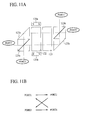
- FIG. 11A is a conceptual view of a structure of the previously-proposed optical circulator.
- FIG. 11B is a conceptual view of an operation of the optical circulator shown in FIG. 11A.
- the optical circulator comprises a Faraday rotation element 122, a half-wave plate 123, polarization beam slitters 125a, 125b, and mirrors 127a, 127b.
- optical circuit devices comprising optical elements, such as a semiconductor laser, semiconductor receiving optics, an optical modulator, a semiconductor light amplifier, an optical multiplexer, an optical branching filter, etc., formed on one and the same substrate have been proposed. All of such optical elements can be formed of compound semiconductors, and can be integrated on one and the same compound semiconductor substrate.
- III-V group compound semiconductor substrates such as InP substrates, InGaAs substrates, GaAs substrates, etc., are used.
- yttrium iron garnet the material that the above-described Faraday rotation element 122 is formed of, is a material which is very difficult to be used on III-V group compound semiconductor substrates, such as InP substrates, etc.
- the Faraday rotation element 122 is formed of yttrium iron garnet, the Faraday rotation element 122 and a semiconductor laser, etc. cannot be integrated on one and the same compound semiconductor substrate.
- the Faraday rotation element of the proposed II-VI group magnetic semiconductor is usable only for light of a short wavelength region and is not usable for the light of a long-wavelength region, as of, for example, a 1.3 ⁇ m-band and a 1.55 ⁇ m-band.
- the II-VI group magnetic semiconductor cannot be grown to have good crystallinity, which results in large light loss. Accordingly, when a material of the Faraday rotation element is a II-VI group magnetic semiconductor, it is difficult to provide an optical circuit device comprising the Faraday rotation element and a semiconductor laser integrated on one and the same III-V group compound semiconductor substrate.
- the III-V group magnetic semiconductor containing MnAs has large photoabsorption, low Curie temperature, and does not have good crystallinity.
- a material of the Faraday rotation element is MnAs content-III-V group magnetic semiconductor, it is difficult to provide an optical circuit device comprising the Faraday rotation element and a semiconductor laser integrated on one and the same III-V group compound semiconductor substrate.
- an optical circuit device which permits a Faraday rotation element, a semiconductor laser, etc. integrated on one and the same compound semiconductor, and a method for fabricating such an optical circuit device.
- an optical circuit device comprising; a substrate of a III-V group compound semiconductor; and a magnetic semiconductor layer formed on the substrate, substantially lattice matching with the substrate and having a chalcopyrite type crystal structure.
- a method for fabricating an optical circuit device comprising the step of forming on the substrate of a III-V group compound semiconductor, a magnetic semiconductor layer which substantially lattice matches with the substrate and has a chalcopyrite type crystal structure.
- the Faraday rotation element which is good, can have small light loss and can be micronized, can be formed on a III-V group semiconductor substrate. Furthermore, according to an embodiment of the present invention, the waveguide layer forming the Faraday rotation element is formed in a mesa, which permits an optical circuit device embodying the present invention to have good coupling efficiency.
- a Faraday rotation element is formed on a III-V group semiconductor substrate, which is widely used as the substrate of semiconductor lasers, etc., allowing the optical circuit device to have a semiconductor laser, an optical isolator, etc. integrated on one and the same III-V group semiconductor substrate.
- III-V group compound semiconductor substrates such as InP substrates, In X Ga 1-X As substrates, GaAS substrates, etc. have not yet been proposed.
- the inventor of the present invention has made earnest studies and had an idea of using as a material of the Faraday rotation element, a magnetic semiconductor with a chalcopyrite type crystal structure, which can lattice-match with III-V group compound semiconductor substrates.
- a magnetic semiconductor having the chalcopyrite type crystal structure is a material which can provide the Faraday effect, and can therefore be used to form the Faraday rotation element. Furthermore, a magnetic semiconductor having the chalcopyrite type crystal structure that is lattice-matched with substrates, has fewer crystal defects, which can make light loss from the Faraday rotation element small. A magnetic semiconductor of the chalcopyrite type crystal structure can provide a large Verdet's constant, which makes it possible to reduce a length of the Faraday rotation element, and thus makes it possible to micronize an optical circuit device containing such a Faraday rotation element.
- the inventor of the present invention has searched after, in the following way, a magnetic semiconductor of the chalcopyrite type crystal structure which can lattice-match with III-V group compound semiconductor substrates.
- a magnetic semiconductor of the chalcopyrite type crystal structure which can lattice-match with an InP substrate will be explained.
- the lattice constant of a magnetic semiconductor of the chalcopyrite type crystal structure which contains Mn has not been previously-proposed.
- J.K. Furdyna, JAP 64 (1988) R29 (hereinafter called Reference 1) describes data of anion-cation bond distances of Mn-content II-VI group compound semiconductor mixed crystals.
- Reference 1 J.K. Furdyna, JAP 64 (1988) R29 (hereinafter called Reference 1) describes data of anion-cation bond distances of Mn-content II-VI group compound semiconductor mixed crystals.
- the distance is 3.97 angstrom.
- an anion-cation bond distance of Mn-Se bonds is given, the distance is 4.17 angstrom.
- an anion-cation bond distance of Mn-Te bonds is given, the distance is 4.51 angstrom.
- Reference 2 Linus Pauling, THE NATURE OF THE CHEMICAL BOND, Cornell University Press, New York, 1960 (hereinafter called Reference 2) describes the tetrahedral covalent radius of S, Se, Te.
- a tetrahedral covalent radius of the S is 1.04 angstrom
- a tetrahedral covalent radius of the Te is 1.32 angstrom.
- the tetrahedral covalent radius is 1.42 angstrom.
- Reference 2 describes the tetrahedral covalent radius of Zn, Cd, In, Ga, Si, Ge, Sn, P, As, Sb, etc.
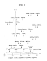
- FIG. 1 is a view of the average bond distances of the anion-cation bond distances of the respective compound crystals.
- the horizontal axis in FIG. 1 denotes the average bond distances of the anion-cation bond distances.
- the view means nothing in the vertical direction, and the broken line indicates the anion-cation bond distance of InP crystals.
- FIG. 1 shows not only the average anion-cation bond distance of the crystals of compounds of the chalcopyrite type crystal structure (hereinafter called chalcopyrite type compounds), but also the average anion-cation bond distance of compounds of zinc blende type crystal structure (hereinafter called zinc blende type compounds).
- the zinc blende type compounds are enclosed with the dot line.
- a quaternary compound of the chalcopyrite type crystal structure which contains Mn as a transition metal element and can lattice-match with the InP substrate is given as follows by using FIG. 1.
- the quaternary compound of the chalcopyrite type crystal structure can be prepared by combining ternary compounds (hereinafter also called chalcopyrite type ternary compounds) which have a symmetrical positional relationship with respect to the broken line in FIG. 1, at least one of which contains Mn, which have two common elements and which have the chalcopyrite type crystal structure.
- the crystals of compounds given by combining the compounds symmetrically positioned with respect to the broken line in FIG. 1 have anion-cation bond distances indicated by the broken line in FIG. 1.
- the position indicated by the broken line in FIG. 1 is the average anion-cation bond distance of InP.
- the average anion-cation bond distances of the crystals of the compounds prepared by such combination are substantially equal to the average anion-cation bond distance of InP crystals. Accordingly, the crystals of the compounds prepared by such combination lattice-match with InP. Because at least one of the chalcopyrite type ternary compounds used in the combination contains Mn, a quaternary compound of the chalcopyrite type crystal structure (hereinafter also called a chalcopyrite type quaternary compound) given by such combination contains Mn as a transition metal element. Because the chalcopyrite type ternary compounds used in the combination are common in two elements, a compound prepared by the combination is a quaternary compound.
- the quaternary compound of the chalcopyrite type crystal structure can be prepared by combining compounds which have a symmetrical positional relationship with respect to the broken line in FIG. 1, one of which is the chalcopyrite type compound containing Mn, the other of which is a zinc blende type compound containing a V group element which is in common with the chalcopyrite type compound. Even the combination of such compounds can prepare a chalcopyrite type quaternary compound which contains Mn as a transition metal element and can lattice match with InP substrates.
- the chalcopyrite type quaternary compounds thus prepared are largely divided in (T 0.5 IV 0.5 ) X III 1-X V type, T 0.5 (IV X IV' 1-X ) 0.5 V type, T 0.5 IV 0.5 V X V' 1-X type and (II X T 1-X ) 0.5 IV 0.5 V type.
- T represents a transition metal element; II indicates a II group element; III denotes a III group element; IV and IV' represent a IV group element; V and V' indicate a V group element.
- II 0.5 IV 0.5 V type and II-IV-V 2 type are synonymous.
- a composition ratio X of (Mn 0.5 Si 0.5 ) X In 1-X As for the lattice-matching with InP is 0.54 in computation.
- the composition ratio X is suitably set in the range of 0.44 to 0.64, whereby (Mn 0.5 Si 0.5 ) X In 1-X As which substantially lattice-matches with InP can be prepared.
- a composition ratio X of (Mn 0.5 Ge 0.5 ) X In 1-X As for the lattice-matching with InP is 0.66 in computation.
- the composition ratio X is suitably set in the range of 0.56 to 0.76, whereby (Mn 0.5 Ge 0.5 ) X In 1-X As which substantially lattice-matches with InP can be prepared.
- a composition ratio X of (Mn 0.5 Sn 0.5 ) X Ga 1-X As for the lattice-matching with InP is 0.67 in computation.
- the composition ratio X is suitably set in the range of 0.57 to 0.77, whereby (Mn 0.5 Sn 0.5 ) X Ga 1-X As which substantially lattice-matches with InP can be prepared.
- a composition ratio X of (Mn 0.5 (Si X Sn 1-X ) 0.5 )As for the lattice-matching with InP is 0.42 in computation.
- the composition ratio X is suitably set in the range of 0.32 to 0.52, whereby (Mn 0.5 (Si X Sn 1-X ) 0.5 )As which substantially lattice-matches with InP can be prepared.
- a composition ratio X of (Mn 0.5 (Ge X Sn 1-X ) 0.5 )As for the lattice-matching with InP is 0.54 in computation.
- the composition ratio X is suitably set in the range of 0.44 to 0.64, whereby (Mn 0.5 (Ge X Sn 1-X ) 0.5 )As which substantially lattice-matches with InP can be prepared.
- As chalcopyrite type quaternary compounds of T 0.5 IV 0.5 V X V' 1-X type are considered Mn 0.5 Si 0.5 P X Sb 1-X , Mn 0.5 Si 0.5 As X Sb 1-X , Mn 0.5 Ge 0.5 P X Sb 1-X , Mn 0.5 Ge 0.5 As X Sb 1-X , Mn 0.5 Sn 0.5 P X As 1-X and Mn 0.5 Sn 0.5 P X Sb 1-X .
- a composition ratio X of Mn 0.5 Si 0.5 P X Sb 1-X for the lattice-matching with InP is 0.44 in computation.
- the composition ratio X is suitably set in the range of 0.34 to 0.54, whereby Mn 0.5 Si 0.5 P X Sb 1-X which substantially lattice-matches with InP can be prepared.
- a composition ratio X of Mn 0.5 Si 0.5 As X Sb 1-X for the lattice-matching with InP is 0.63 in computation.
- the composition ratio X is suitably set in the range of 0.53 to 0.73, whereby Mn 0.5 Si 0.5 As X Sb 1-X which substantially lattice-matches with InP can be prepared.
- a composition ratio X of Mn 0.5 Ge 0.5 P X Sb 1-X for the lattice-matching with InP is 0.53 in computation.
- the composition ratio X is suitably set in the range of 0.43 to 0.63, whereby Mn 0.5 Ge 0.5 P X Sb 1-X which substantially lattice-matches with InP can be prepared.
- a composition ratio X of Mn 0.5 Ge 0.5 As X Sb 1-X for the lattice-matching with InP is 0.77 in computation.
- the composition ratio X is suitably set in the range of 0.67 to 0.87, whereby Mn 0.5 Ge 0.5 As X Sb 1-X which substantially lattice-matches with InP can be prepared.
- a composition ratio X of Mn 0.5 Sn 0.5 P X As 1-X for the lattice-matching with InP is 0.60 in computation.
- the composition ratio X is suitably set in the range of 0.50 to 0.70, whereby Mn 0.5 Sn 0.5 P X As 1-X which substantially lattice-matches with InP can be prepared.
- a composition ratio X of Mn 0.5 Sn 0.5 P X Sb 1-X for the lattice-matching with InP is 0.88 in computation.
- the composition ratio X is suitably set in the range of 0.78 to 0.98, whereby Mn 0.5 Sn 0.5 P X Sb 1-X which substantially lattice-matches with InP can be prepared.
- a composition ratio X of (Zn X Mn 1-X ) 0.5 Sn 0.5 As for the lattice-matching with InP is 0.91 in computation.
- the composition ratio X is suitably set in the range of 0.81 to 1, whereby (Zn X Mn 1-X ) 0.5 Sn 0.5 As which substantially lattice-matches with InP can be prepared.
- chalcopyrite type compounds which can lattice match with InP are not essentially limited to quaternary compounds but may be five or more elements chalcopyrite type compounds which can be prepared by mixing the above-described quaternary chalcopyrite type compounds by arbitrary ratios.
- the chalcopyrite type quaternary compounds prepared by the above-described combinations substantially lattice match with InP, and the five or more elements chalcopyrite type compounds prepared by combining the chalcopyrite type quaternary compounds prepared by the above-described combinations can lattice match with InP.
- the InGaAs substrates will be exemplified by the In 0.3 Ga 0.7 As substrate.
- a transition metal element will be exemplified by Mn, as described above.
- FIG. 2 is a view of average anion-cation bond distances of the crystals of respective compounds.
- the broken line indicates the average anion-cation bond distance of the crystals of In 0.3 Ga 0.7 As.
- FIG. 2 is the same as FIG. 1 except that the broken line indicates the average anion-cation bond distance of the crystal of In 0.3 Ga 0.7 As.
- Chalcopyrite quaternary compounds which contain Mn as a transition metal element and can lattice match with In 0.3 Ga 0.7 As can be given by using FIG. 2 in the same way as described above.
- the chalcopyrite type quaternary compounds prepared by such combination are largely divided in (T 0.5 IV 0.5 ) X III 1-X V type, T 0.5 (IV X IV' 1-X ) 0.5 V type, T 0.5 IV 0.5 V X V' 1-X type and (II X T 1-X ) 0.5 IV 0.5 V type.
- a composition ratio X of (Mn 0.5 Si 0.5 ) X In 1-X P for the lattice matching with In 0.3 Ga 0.7 As is 0.31 in computation.
- the composition ratio X is suitably adjusted in the range of 0.21 to 0.41, whereby (Mn 0.5 Si 0.5 ) X In 1-X P which substantially lattice matches with In 0.3 Ga 0.7 As can be prepared.
- a composition ratio X of (Mn 0.5 Ge 0.5 ) X In 1-X P for the lattice matching with In 0.3 Ga 0.7 As is 0.38 in computation.
- the composition ratio X is suitably adjusted in the range of 0.28 to 0.48, whereby (Mn 0.5 Ge 0.5 ) X In 1-X P which substantially lattice matches with In 0.3 Ga 0.7 As can be prepared.
- a composition ratio X of (Mn 0.5 Sn 0.5 ) X Ga 1-X P for the lattice matching with In 0.3 Ga 0.7 As is 0.90 in computation.
- the composition ratio X is suitably adjusted in the range of 0.80 to 1, whereby (Mn 0.5 Sn 0.5 ) X Ga 1-X P which substantially lattice matches with In 0.3 Ga 0.7 As can be prepared.
- a composition ratio X of (Mn 0.5 Si 0.5 ) X In 1-X As for the lattice matching with In 0.3 Ga 0.7 As is 0.86 in computation.
- the composition ratio X is suitably adjusted in the range of 0.76 to 0.96, whereby (Mn 0.5 Si 0.5 ) X In 1-X As which substantially lattice matches with In 0.3 Ga 0.7 As can be prepared.
- a composition ratio X of (Mn 0.5 Ge 0.5 ) X Ga 1-X As for the lattice matching with In 0.3 Ga 0.7 As is 0.92 in computation.
- the composition ratio X is suitably adjusted in the range of 0.82 to 1, whereby (Mn 0.5 Ge 0.5 ) X Ga 1-X As which substantially lattice matches with In 0.3 Ga 0.7 As can be prepared.
- a composition ratio X of (Mn 0.5 Sn 0.5 ) X Ga 1-X As for the lattice matching with In 0.3 Ga 0.7 As is 0.36 in computation.
- the composition ratio X is suitably adjusted in the range of 0.26 to 0.46, whereby (Mn 0.5 Sn 0.5 ) X Ga 1-X As which substantially lattice matches with In 0.3 Ga 0.7 As can be prepared.
- a composition ratio X of (Mn 0.5 (Si X Sn 1-X ) 0.5 )P for the lattice matching with In 0.3 Ga 0.7 As is 0.12 in computation.
- the composition ratio X is suitably adjusted in the range of 0.02 to 0.22, whereby (Mn 0.5 (Si X Sn 1-X ) 0.5 )P which substantially lattice matches with In 0.3 Ga 0.7 As can be prepared.
- a composition ratio X of (Mn 0.5 (Ge X Sn 1-X ) 0.5 )P for the lattice matching with In 0.3 Ga 0.7 As is 0.16 in computation.
- the composition ratio X is suitably adjusted in the range of 0.06 to 0.26, whereby (Mn 0.5 (Ge X Sn 1-X ) 0.5 )P which substantially lattice matches with In 0.3 Ga 0.7 As can be prepared.
- a composition ratio X of (Mn 0.5 (Si X Ge 1-X ) 0.5 )As for the lattice matching with In 0.3 Ga 0.7 As is 0.17 in computation.
- the composition ratio X is suitably adjusted in the range of 0.07 to 0.27, whereby (Mn 0.5 (Si X Ge 1-X ) 0.5 )As which substantially lattice matches with In 0.3 Ga 0.7 As can be prepared.
- a composition ratio X of (Mn 0.5 (Si X Sn 1-X ) 0.5 )As for the lattice matching with In 0.3 Ga 0.7 As is 0.82 in computation.
- the composition ratio X is suitably adjusted in the range of 0.72 to 0.92, whereby (Mn 0.5 (Si X Sn 1-X ) 0.5 ) As which substantially lattice matches with In 0.3 Ga 0.7 As can be prepared.
- As chalcopyrite type quaternary compounds of T 0.5 IV 0.5 V X V' 1-X type are considered Mn 0.5 Si 0.5 P X Sb 1-X , Mn 0.5 Si 0.5 As X Sb 1-X , Mn 0.5 Ge 0.5 P X As 1-X , and Mn 0.5 Ge 0.5 P X Sb 1-X .
- a composition ratio X of Mn 0.5 Si 0.5 P X Sb 1-X for the lattice matching with In 0.3 Ga 0.7 As is 0.61 in computation.
- the composition ratio X is suitably adjusted in the range of 0.51 to 0.71, whereby Mn 0.5 Si 0.5 P X Sb 1-X which substantially lattice matches with In 0.3 Ga 0.7 As can be prepared.
- a composition ratio X of Mn 0.5 Si 0.5 As X Sb 1-X for the lattice matching with In 0.3 Ga 0.7 As is 0.88 in computation.
- the composition ratio X is suitably adjusted in the range of 0.78 to 0.98, whereby Mn 0.5 Si 0.5 As X Sb 1-X which substantially lattice matches with In 0.3 Ga 0.7 As can be prepared.
- a composition ratio X of Mn 0.5 Ge 0.5 P X AS 1-X for the lattice matching with In 0.3 Ga 0.7 As is 0.05 in computation.
- the composition ratio X is suitably adjusted in the range of 0 to 0.15, whereby Mn 0.5 Ge 0.5 P X As 1-X which substantially lattice matches with In 0.3 Ga 0.7 As can be prepared.
- a composition ratio X of Mn 0.5 Ge 0.5 P X Sb 1-X for the lattice matching with In 0.3 Ga 0.7 As is 0.71 in computation.
- the composition ratio X is suitably adjusted in the range of 0.61 to 0.81, whereby Mn 0.5 Ge 0.5 P X Sb 1-X which substantially lattice matches with In 0.3 Ga 0.7 As can be prepared.
- a composition ratio X of (Zn X Mn 1-X ) 0.5 Sn 0.5 P for the lattice matching with In 0.3 Ga 0.7 As is 0.27 in computation.
- the composition ratio X is suitably adjusted in the range of 0.17 to 0.37, whereby (Zn X Mn 1-X ) 0.5 Sn 0.5 P which substantially lattice matches with In 0.3 Ga 0.7 As can be prepared.
- a composition ratio X of (Zn X Mn 1-X ) 0.5 Ge 0.5 As for the lattice matching with In 0.3 Ga 0.7 As is 0.08 in computation.
- the composition ratio X is suitably adjusted in the range of 0 to 0.18, whereby (Zn X Mn 1-X ) 0.5 Ge 0.5 As which substantially lattice matches with In 0.3 Ga 0.7 As can be prepared.
- a composition ratio X of (Cd X Mn 1-X ) 0.5 Si 0.5 As for the lattice matching with In 0.3 Ga 0.7 As is 0.65 in computation.
- the composition ratio X is suitably adjusted in the range of 0.55 to 0.75, whereby (Cd X Mn 1-X ) 0.5 Si 0.5 As which substantially lattice matches with In 0.3 Ga 0.7 As can be prepared.
- composition ratio X of the In X Ga 1-X As substrates is not essentially limited to 0.3 and may be suitably set in the range of, e.g., 0.2 to 0.4. Even when the composition ratio is suitably set in the range of 0.2 to 0,4, the above-described chalcopyrite type quaternary compounds can substantially lattice match with the InGaAs substrates.
- chalcopyrite type compounds which can lattice match with InGaAs are not essentially limited to quaternary compounds but may be five or more elements chalcopyrite type compounds which can be prepared by mixing the above-described chalcopyrite type quaternary compounds by arbitrary ratios.
- the chalcopyrite type quaternary compounds prepared by the above-described combinations substantially lattice match with InGaAs, and the five or more elements chalcopyrite type compounds prepared by combining the chalcopyrite type quaternary compounds prepared by the above-described combinations can lattice match with InGaAs.
- a transition metal element will be exemplified by Mn, as described above.
- FIG. 3 is a view of average anion-cation bond distances of the crystals of respective compounds.
- the broken line indicates the anion-cation bond distance of the crystals of GaAs.
- FIG. 3 is the same as FIGS. 1 and 2 except that the broken line indicates the anion-cation bond distance of the crystal of GaAs.
- Chalcopyrite quaternary compounds which contain Mn as a transition metal element and can lattice match with GaAs can be given by using FIG. 3 in the same way as described above.
- the chalcopyrite type quaternary compounds prepared by such combination are largely divided in (T 0.5 IV 0.5 ) X III 1-X V type, T 0.5 (IV X IV' 1-X ) 0.5 V type, T 0.5 IV 0.5 V X V' 1-X type and (II X T 1-X ) 0.5 IV 0.5 V type, as described above.
- a composition ratio X of (Mn 0.5 Si 0.5 ) X In 1-X P for the lattice matching with GaAs is 0.68 in computation.
- the composition ratio X is suitably adjusted in the range of 0.58 to 0.78, whereby (Mn 0.5 Si 0.5 ) X In 1-X P which substantially lattice matches with GaAs can be prepared.
- a composition ratio X of (Mn 0.5 Ge 0.5 ) X In 1-X P for the lattice matching with GaAs is 0.82 in computation.
- the composition ratio X is suitably adjusted in the range of 0.72 to 0.92, whereby (Mn 0.5 Ge 0.5 ) X In 1-X P which substantially lattice matches with GaAs can be prepared.
- a composition ratio X of (Mn 0.5 Sn 0.5 ) X Ga 1-X P for the lattice matching with GaAs is 0.54 in computation.
- the composition ratio X is suitably adjusted in the range of 0.44 to 0.64, whereby (Mn 0.5 Sn 0.5 ) X Ga 1-X P which substantially lattice matches with GaAs can be prepared.
- a composition ratio X of (Mn 0.5 (Si X Sn 1-X ) 0.5 )P for the lattice matching with GaAs is 0.59 in computation.
- the composition ratio X is suitably adjusted in the range of 0.49 to 0.69, whereby (Mn 0.5 (Si X Sn 1-X ) 0.5 ) P which substantially lattice matches with GaAs can be prepared.
- a composition ratio X of (Mn 0.5 (Ge X Sn 1-X ) 0.5 )P for the lattice matching with GaAs is 0.76 in computation.
- the composition ratio X is suitably adjusted in the range of 0.66 to 0.86, whereby (Mn 0.5 (Ge X Sn 1-X ) 0.5 )P which substantially lattice matches with GaAs can be prepared.
- As chalcopyrite type quaternary compounds of T 0.5 IV 0.5 V X V' 1-X type are considered Mn 0.5 Si 0.5 P X As 1-X , Mn 0.5 Si 0.5 P X Sb 1-X , Mn 0.5 Ge 0.5 P X As 1-X and Mn 0.5 Ge 0.5 P X Sb 1-X .
- a composition ratio X of Mn 0.5 Si 0.5 P X As 1-X for the lattice matching with GaAs is 0.41 in computation.
- the composition ratio X is suitably adjusted in the range of 0.31 to 0.51, whereby Mn 0.5 Si 0.5 P X As 1-X which substantially lattice matches with GaAs can be prepared.
- a composition ratio X of Mn 0.5 Si 0.5 P X Sb 1-X for the lattice matching with GaAs is 0.82 in computation.
- the composition ratio X is suitably adjusted in the range of 0.72 to 0.92, whereby Mn 0.5 Si 0.5 P X Sb 1-X which substantially lattice matches with GaAs can be prepared.
- a composition ratio X of Mn 0.5 Ge 0.5 P X As 1-X for the lattice matching with GaAs is 0.73 in computation.
- the composition ratio X is suitably adjusted in the range of 0.63 to 0.83, whereby Mn 0.5 Ge 0.5 P X As 1-X which substantially lattice matches with GaAs can be prepared.
- a composition ratio X of Mn 0.5 Ge 0.5 P X Sb 1-X for the lattice matching with GaAs is 0.92 in computation.
- the composition ratio X is suitably adjusted in the range of 0.82 to 1, whereby Mn 0.5 Ge 0.5 P X Sb 1-X which substantially lattice matches with GaAs can be prepared.
- a composition ratio X of (Zn X Mn 1-X ) 0.5 Si 0.5 As for the lattice matching with GaAs is 0.62 in computation.
- the composition ratio X is suitably adjusted in the range of 0.52 to 0.72, whereby (Zn X Mn 1-X ) 0.5 Si 0.5 As which substantially lattice matches with GaAs can be prepared.
- a composition ratio X of (Cd X Mn 1-X ) 0.5 Ge 0.5 P for the lattice matching with GaAs is 0.69 in computation.
- the composition ratio X is suitably adjusted in the range of 0.59 to 0.79, whereby (Cd X Mn 1-X ) 0.5 Ge 0.5 P which substantially lattice matches with GaAs can be prepared.
- chalcopyrite type compounds which can lattice match with GaAs are not essentially limited to quaternary compounds but may be five or more elements chalcopyrite type compounds which can be prepared by mixing the above-described chalcopyrite type quaternary compounds by arbitrary ratios.
- the chalcopyrite type quaternary compounds prepared by the above-described combinations substantially lattice match with GaAs, and the five or more elements chalcopyrite type compounds prepared by combining the chalcopyrite type quaternary compounds prepared by the above-described combinations can lattice match with GaAs.
- FIG. 4 is a perspective view of an optical circuit device according to the present embodiment.
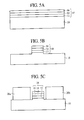
- FIGs. 5A to 5C are sectional views of an optical circuit device according to the present embodiment to explain the steps of a method embodying the present invention for fabricating the same.
- a lower clad layer 12 of, e.g., a 1 ⁇ m-InP layer is formed on an InP substrate 10.
- the thickness of the lower clad layer 12 is not limited to 1 ⁇ m and may be suitably set in the range of, e.g., 0.1 to 10 ⁇ m.
- a core layer 14 of, e.g., a 0.5 ⁇ m-(Mn 0.5 Si 0.5 ) 0.54 In 0.46 As is formed on the lower clad layer 12.
- (Mn 0.5 Si 0.5 ) 0.54 In 0.46 As contains Mn as the transition metal element and is a magnetic semiconductor of the chalcopyrite type crystal structure which can lattice match with the InP substrate 10.
- a material of the core layer is exemplified by (Mn 0.5 Si 0.5 ) X In 1-X As.
- the material of the core layer is not limited to (Mn 0.5 Si 0.5 ) X In 1-X As, and the above-described chalcopyrite type compounds which can lattice match with the InP substrate 10 can be suitably used.
- the thickness of the core layer 14 is not limited to 0.5 ⁇ m and may be suitably set in the range of, e.g., 0.01 to 1 ⁇ m.
- An upper clad layer 16 of, e.g., a 1 ⁇ m-InP layer is formed on the core layer 14.
- the thickness of the upper clad layer 16 is not limited to 1 ⁇ m and may be suitably set in the range of 1 to 10 ⁇ m.
- the lower clad layer 12, the core layer 14 and the upper clad layer 16 form an optical waveguide layer 18.
- the optical waveguide layer 18 is formed in a mesa.
- the optical waveguide layer 18 is mesa-shaped for small light loss and good coupling with other optical elements.
- a length of the optical waveguide layer 18 is set to be, e.g., 1 mm.
- the length of the optical waveguide layer 18 is not limited to 1 mm and can be suitably set in the range of, e.g., 100 ⁇ m to 10 mm.
- Permanent magnets 20a, 20b are disposed on the InP substrate 10 on both sides of the mesa-shaped optical waveguide layer 18.
- the permanent magnets 20a, 20b apply magnetic fields to the optical waveguide layer 18.
- a magnetic semiconductor of the chalcopyrite type crystal structure when used as a material of the core layer 14, can cause the Faraday effect, as described above. Accordingly, the optical waveguide layer 18 including such a magnetic semiconductor as the core layer 14 can form a Faraday rotation element 22 which can rotate a deflection angle by 45 degrees.
- An optical circuit device has such structure.
- Such a Faraday rotation element 22 can be combined with a polarizer (not shown), etc. to thereby form an optical isolator.
- a Faraday rotation element 22 is combined with a half-wave plate (not shown), a polarization beam slitter (not shown), etc. to thereby form an optical circulator.
- an optical circuit device is characterized mainly in that a material of the Faraday rotation element 22 is a magnetic semiconductor of the chalcopyrite type crystal structure which can lattice match with the InP substrate 10.
- a magnetic semiconductor of the chalcopyrite type crystal structure which can lattice match with the InP substrate 10 is a material which can cause the Faraday effect, and can be used to form the Faraday rotation element 22. Furthermore, a magnetic semiconductor that is lattice-matched with the InP substrate 10 and has the chalcopyrite type crystal structure, has fewer crystal defects and, accordingly, can form a Faraday rotation element of small light loss.
- a magnetic semiconductor of the chalcopyrite type crystal structure can have a large Verdet's constant, which allows the Faraday rotation element 22 to be shorter, with a result that the optical circuit device can be micronized.
- a Faraday rotation element 22 which is good, can have small light loss and can be micronized can be formed on the InP substrate 10. Furthermore, according to the present embodiment, the optical waveguide layer 18 forming the Faraday rotation element 22 is formed in a mesa, which permits the optical circuit device to have good coupling efficiency.
- the Faraday rotation element 22 is formed on the InP substrate 10, that is widely used as substrates of semiconductor lasers, etc., which allows the optical circuit device to have a semiconductor laser, an optical isolator, etc. integrated on one and the same InP substrate 10.
- the lower clad layer 12 is formed of, e.g., a 1 ⁇ m-thickness InP on the entire surface of an InP substrate 10 by MOCVD (Metal Organic Chemical Vapor Deposition).
- MOCVD Metal Organic Chemical Vapor Deposition
- the thickness of the lower clad layer is not limited to 1 ⁇ m and can be suitably set in the range of, e.g., 0.1 to 10 ⁇ m.
- the core layer 14 is formed of e.g., a 0.5 ⁇ m-thickness (Mn 0.5 Si 0.5 ) 0.54 In 0.46 As on the entire surface by MOCVD.
- the material of the core layer 14 is not limited to (Mn 0.5 Si 0.5 ) 0.54 In 0.46 As, and the above-described chalcopyrite type compounds, which can lattice match with the InP substrate 10 can be suitably used.
- the thickness of the core layer 14 is not limited to 0.5 ⁇ m and can be suitably set in the range of, e.g., 0.01 to 1 ⁇ m.
- the upper clad layer 16 is formed of, e.g., 1 ⁇ m-thickness InP film on the entire surface by MOCVD.
- the thickness of the upper clad layer 16 is not limited to 1 ⁇ m and can be suitably set in the range of, e.g., 0.1 to 10 ⁇ m.
- the lower clad layer 12, the core layer 14 and the upper clad layer 16 form a layer film 17.
- the layer film 17 is patterned in a mesa by dry etching using photolithography.
- the mesa-shaped optical waveguide layer 18 is formed.
- the permanent magnets 20a, 20b are disposed on the InP substrate 10 on both sides of the mesa-shaped optical waveguide 18.
- an optical circuit device is fabricated.
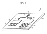
- FIG. 6 is a perspective view of an optical circuit device according to the present modification.
- An optical circuit device is characterized mainly in that an optical isolator 24 comprises the Faraday rotation element 22 shown in FIG. 4, and a semiconductor laser 26, etc. are further formed on one and the same InP substrate 10.
- the optical isolator 24 provided by the Faraday rotation element shown in FIG. 4 can be used in the multiwavelength transceiver 28 but also in any other optical circuit device.
- the semiconductor laser 26, the light isolator 24, light couplers 30, 32, semiconductor light amplifiers 34, 36, an optical branching filter 38, and a photodiode 40 are formed on the InP substrate 10. These optical elements are optically connected by the optical waveguide 42.
- the optical isolator 24 includes polarizers (not shown) combined on both ends of the Faraday rotation element 22 shown in FIG. 4.
- the optical isolator 24 is disposed on the output side of the semiconductor laser 26 to thereby prohibit the reflected light from returning to the semiconductor laser 26.
- An optical circuit device is thus constituted.
- an optical circuit device including the optical isolator 24, the semiconductor laser 26, etc. integrated on one and the same InP substrate 10 can be provided.
- FIG. 7 is a perspective view of an optical circuit device according to the second modification.
- An optical circuit device is characterized mainly in that an optical circulator 44 comprises the Faraday rotation element 22 shown in FIG. 4, and a semiconductor laser 46, etc. are further formed on one and the same InP substrate 10.
- the present modification is exemplified by a photosignal regenerator 48 including the optical circulator 44, the semiconductor laser 46, etc. integrated on one and the same InP substrate 10.
- the optical circulator 44 comprising the Faraday rotation element 22 shown in FIG. 4 can be used not only in the photosignal regenerator 48 but also in any other optical circuit device.
- semiconductor light amplifiers 50, 52, the semiconductor laser 46, and the optical circulator 44 are formed on the InP substrate 10. These optical elements are optically connected by an optical waveguide 54.
- the optical circulator 44 includes a half-wave plate (not shown), a polarization beam splitter (not shown), etc. combined with the Faraday rotation element 22 shown in FIG. 4.
- the semiconductor laser 46 comprises a mode-locked laser.
- An optical circuit device has such a structure.
- a photosignal whose waveform and timing have been deformed and disordered in transmission is divided in three photosignals. Suitable phase shifts are set for these photosignals to introduce the respective photosignals into input ports A, B, C. Then, a photosignal having the waveform and the timing adjusted, i.e., a regenerated photosignal, is outputted from an output port.
- an optical circuit device can include the semiconductor laser 46 and the optical circulator 44 integrated on one and the same InP substrate 10.
- FIG. 8 shows a perspective view of such an optical circuit device.
- the same members of the present embodiment as those of an optical circuit device according to the first embodiment, and a method embodying the present invention for fabricating the same, are represented by the same reference numbers so as not to repeat and to simplify their explanation.
- An optical circuit device is characterized mainly in that an In 0.3 Ga 0.7 As substrate 10a is used.
- a lower clad layer 12a of, e.g., a 1 ⁇ m-thickness In 0.77 Ga 0.23 P is formed on the monocrystal In 0.3 Ga 0.7 As substrate 10a.
- a core layer 14a of, e.g., 0.5 ⁇ m-thickness (Mn 0.5 Si 0.5 ) 0.86 In 0.14 As is formed on the lower clad layer 12.
- the material of the core layer 14a is not limited to (Mn 0.5 Si 0.5 ) 0.86 In 0.14 As, and the above-described chalcopyrite type compounds which can substantially lattice match with the In 0.3 Ga 0.7 As substrate 10a can be suitably used.
- An upper clad layer 16a of, e.g., a 1 ⁇ m-thickness In 0.77 Ga 0.23 P is formed on the core layer 14a.
- the lower clad layer 12a, the core layer 14a and the upper clad layer 16a form an optical waveguide layer 18a.
- the optical waveguide layer 18a is formed in a mesa.
- the Faraday rotation element 22a which is good, can have small light loss and can be micronized can be formed on the InGaAs substrate 10a. Furthermore, according to the present embodiment, the waveguide layer 18a forming the Faraday rotation element 22a is formed in a mesa, which permits the optical circuit device to have good coupling efficiency.
- the Faraday rotation element 22a is formed on the InGaAs substrate 10a that is widely used as substrates of semiconductor lasers, etc., which allows the optical circuit device to have a semiconductor laser, an optical isolator, etc. integrated on one and the same InGaAs substrate 10a.
- the optical circuit device according to the present embodiment can be fabricated in substantially the same way as by a method embodying the present invention for fabricating the optical circuit device according to the first embodiment shown in FIG. 5.
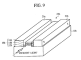
- FIG. 9 is a perspective view of an optical circuit device according to the present embodiment.
- the same members of the present embodiment as those of an optical circuit device according to the first and the second embodiment shown in FIGs. 4 to 8 are represented by the same reference numbers so as not to repeat and to simplify their explanation.
- An optical circuit device is characterized mainly in that a GaAs substrate 10b is used.
- a lower clad layer 12b of, e.g., a 1 ⁇ m-thickness In 0.47 Ga 0.53 P film is formed on a monocrystal GaAs substrate 10b.
- a core layer 14b of, e.g., a 0.5 ⁇ m-thickness (Mn 0.5 Sn 0.5 ) 0.54 Ga 0.46 P film is formed on the lower clad layer 12b.
- the material of the core layer 14b is not limited to (Mn 0.5 Sn 0.5 ) 0.54 Ga 0.46 P, and the above-described chalcopyrite type compounds which can substantially lattice match with the GaAs substrate 10b can be suitably used.
- An upper clad layer 16b of, e.g., a 1 ⁇ m-thickness In 0.47 Ga 0.53 P is formed on the core layer 14b.
- the lower clad layer 12b, the core layer 14b and the upper clad layer 16b form an optical waveguide layer 18b.
- the optical waveguide layer 18b is formed in a mesa.
- the Faraday rotation element 22b which is good, can have small light loss and can be micronized can be formed on the GaAs substrate 10b. Furthermore, according to the present embodiment, the waveguide layer 18b forming the Faraday rotation element 22b is formed in a mesa, which permits the optical circuit device to have good coupling efficiency.
- the Faraday rotation element 22b is formed on the GaAs substrate 10b, that is widely used as substrates of semiconductor lasers, etc., which allows the optical circuit device to have a semiconductor laser, an optical isolator, etc. integrated on one and the same GaAs substrate 10b.
- An optical circuit device according to the present embodiment can be fabricated in substantially the same way as by a method embodying the present invention for fabricating the optical circuit device according to the first embodiment.
- the permanent magnets are disposed on the semiconductor substrate on both sides of the optical waveguide.
- the permanent magnets are not essential, because the core layer of the optical waveguide layer in a device embodying the present invention is formed of a magnetic semiconductor, and the core layer can be magnetized by applying a magnetic field in advance, whereby the Faraday effect can be caused.
- the transition metal element is exemplified by Mn.
- the transition metal element is not limited to Mn and can be another transition metal element, such as Cr, Fe, Co, Ni or others.
- an optical isolator and an optical circulator comprise the Faraday rotation elements 22a, 22b of the second and the third embodiment, and optical elements, such as semiconductor lasers, etc., are formed on one and the same substrates.
- optical circuit devices including the optical isolator, etc. and the semiconductor lasers, etc. integrated on one and the same InGaAs substrate and the GaAs substrate can be provided in an embodiment of the present invention.
Landscapes
- Engineering & Computer Science (AREA)
- Power Engineering (AREA)
- Physics & Mathematics (AREA)
- Nonlinear Science (AREA)
- General Physics & Mathematics (AREA)
- Optics & Photonics (AREA)
- Chemical & Material Sciences (AREA)
- Materials Engineering (AREA)
- Optical Modulation, Optical Deflection, Nonlinear Optics, Optical Demodulation, Optical Logic Elements (AREA)
- Optical Integrated Circuits (AREA)
Abstract
Description
- The present invention relates to an optical circuit device and a method for fabricating an optical circuit device, more specifically to an optical circuit device including a Faraday rotation element, and a method for fabricating the same.
- An optical isolator propagates light in one direction (forward direction) substantially without attenuation and does not propagate the light in the opposite direction (backward direction) and is a non-reciprocity optical device which propagates light in one direction alone.
- A beam exiting a semiconductor laser is reflected outside the semiconductor laser to enter again the semiconductor laser, which makes the operation of the semiconductor laser unstable, resulting in noise increase. To prevent the laser beam from being reflected back into the laser, the optical isolator is disposed on the output side of a semiconductor laser.
- A previously-proposed optical isolator will be explained with reference to FIG. 10 of the accompanying drawings, which shows a conceptual view of such an optical isolator.
- As shown in FIG. 10, the optical isolator comprises a Faraday
rotation element 122,polarizers rotation element 122, andpermanent magnets - In optical communication, light of long wavelength regions, as of, for example, a 1.3 µm-band and a 1.55 µm-band, is used. As the Faraday
rotation element 122 for such long-wavelength regions, bulk yttrium iron garnet (YIG) is generally used. - Of forward light incident on the
polarizer 119a, only a component on the polarization plane of thepolarizer 119a passes through thepolarizer 119a to be introduced into the Faradayrotation element 122. Forward light introduced into the Faradayrotation element 122 exits through thepolarizer 119b because the polarization plane is rotated by 45 degrees due to the Faraday effect. - On the other hand, of backward light, which is reflected light, a component on the polarization plane of the
polarizer 119a passes through thepolarizer 119a to be introduced into the Faradayrotation element 122. The backward light introduced into the Faradayrotation element 122 does not exit the polarizer because the polarization plane is rotated by 45 degrees in a direction opposite to a direction for the forward light, and the polarization plane of the polarizer is offset by 90 degrees. - Thus, the optical isolator can transmit light in only one direction.
- As an optical element using the Faraday rotation element, an optical circulator has been previously-proposed.
- In the optical circulator, incident light and exit light circulate, and the optical circulator is a non-reciprocity optical device having the function of isolating the incident light and the exit light from each other.
- A previously-proposed optical circulator will be explained with reference to FIGs. 11A and 11B of the accompanying drawings, which show conceptual views of such an optical circulator. FIG. 11A is a conceptual view of a structure of the previously-proposed optical circulator. FIG. 11B is a conceptual view of an operation of the optical circulator shown in FIG. 11A.
- As shown in FIG. 11A, the optical circulator comprises a Faraday
rotation element 122, a half-wave plate 123,polarization beam slitters mirrors - In such an optical circulator, as shown in FIG. 11B, light incident on a
port 1 exits only at a port 2, light incident on the port 2 exits only at a port 3, light incident on the port 3 exits only at a port 4, and light incident on the port 4 exits only at theport 1. - On the other hand, recently, optical circuit devices comprising optical elements, such as a semiconductor laser, semiconductor receiving optics, an optical modulator, a semiconductor light amplifier, an optical multiplexer, an optical branching filter, etc., formed on one and the same substrate have been proposed. All of such optical elements can be formed of compound semiconductors, and can be integrated on one and the same compound semiconductor substrate. In integrating semiconductor lasers of a 1.3 µm-band and a 1.55 µm-band used in optical communication, III-V group compound semiconductor substrates, such as InP substrates, InGaAs substrates, GaAs substrates, etc., are used.
- However, yttrium iron garnet, the material that the above-described Faraday
rotation element 122 is formed of, is a material which is very difficult to be used on III-V group compound semiconductor substrates, such as InP substrates, etc. In a case where the Faradayrotation element 122 is formed of yttrium iron garnet, the Faradayrotation element 122 and a semiconductor laser, etc. cannot be integrated on one and the same compound semiconductor substrate. - Recently, as materials of the Faraday rotation element, the use of II-VI group magnetic semiconductor and III-V group magnetic semiconductor containing MnAs have been proposed.
- However, the Faraday rotation element of the proposed II-VI group magnetic semiconductor is usable only for light of a short wavelength region and is not usable for the light of a long-wavelength region, as of, for example, a 1.3 µm-band and a 1.55 µm-band. In a case where a II-VI group magnetic semiconductor is grown on a III-V group compound semiconductor substrate, the II-VI group magnetic semiconductor cannot be grown to have good crystallinity, which results in large light loss. Accordingly, when a material of the Faraday rotation element is a II-VI group magnetic semiconductor, it is difficult to provide an optical circuit device comprising the Faraday rotation element and a semiconductor laser integrated on one and the same III-V group compound semiconductor substrate.
- The III-V group magnetic semiconductor containing MnAs has large photoabsorption, low Curie temperature, and does not have good crystallinity. When a material of the Faraday rotation element is MnAs content-III-V group magnetic semiconductor, it is difficult to provide an optical circuit device comprising the Faraday rotation element and a semiconductor laser integrated on one and the same III-V group compound semiconductor substrate.
- Accordingly, it is desirable to provide an optical circuit device which permits a Faraday rotation element, a semiconductor laser, etc. integrated on one and the same compound semiconductor, and a method for fabricating such an optical circuit device.
- According to an embodiment of one aspect of the present invention, there is provided an optical circuit device comprising; a substrate of a III-V group compound semiconductor; and a magnetic semiconductor layer formed on the substrate, substantially lattice matching with the substrate and having a chalcopyrite type crystal structure.
- According to an embodiment of another aspect of the present invention, there is provided a method for fabricating an optical circuit device comprising the step of forming on the substrate of a III-V group compound semiconductor, a magnetic semiconductor layer which substantially lattice matches with the substrate and has a chalcopyrite type crystal structure.
- As described above, according to an embodiment of the present invention, the Faraday rotation element which is good, can have small light loss and can be micronized, can be formed on a III-V group semiconductor substrate. Furthermore, according to an embodiment of the present invention, the waveguide layer forming the Faraday rotation element is formed in a mesa, which permits an optical circuit device embodying the present invention to have good coupling efficiency.
- According to an embodiment of the present invention, a Faraday rotation element is formed on a III-V group semiconductor substrate, which is widely used as the substrate of semiconductor lasers, etc., allowing the optical circuit device to have a semiconductor laser, an optical isolator, etc. integrated on one and the same III-V group semiconductor substrate.
- Reference will now be made, by way of example, to the accompanying drawings, in which:
- FIG. 1 is a view of average anion-cation bond distances of respective compounds (Part 1);
- FIG. 2 is a view of average anion-cation bond distances of respective compounds (Part 2);
- FIG. 3 is a view of average anion-cation bond distances of respective compounds (Part 3);
- FIG. 4 is a perspective view of an optical circuit device according to a first embodiment of the present invention;
- FIGs. 5A to 5C are sectional views of an optical circuit device according to the first embodiment of the present invention to explain the steps of a method embodying the present invention for fabricating the same;
- FIG. 6 is a perspective view of an optical circuit device according to a first modification of the first embodiment of the present invention;
- FIG. 7 is a perspective view of an optical circuit device according to a second modification of the first embodiment of the present invention;
- FIG. 8 is a perspective view of an optical circuit device according to a second embodiment of the present invention;
- FIG. 9 is a perspective view of an optical circuit device according to a third embodiment of the present invention;
- FIG. 10 (as described above) is a conceptual view of a previously-proposed optical isolator; and
- FIGS. 11A and 11B are conceptual views of a previously-proposed optical circulator.
-
- First, the principle of the present invention will be explained.
- As described above, a technology forming good Faraday rotation elements on III-V group compound semiconductor substrates, such as InP substrates, InXGa1-XAs substrates, GaAS substrates, etc. have not yet been proposed.
- The inventor of the present invention has made earnest studies and had an idea of using as a material of the Faraday rotation element, a magnetic semiconductor with a chalcopyrite type crystal structure, which can lattice-match with III-V group compound semiconductor substrates.
- A magnetic semiconductor having the chalcopyrite type crystal structure is a material which can provide the Faraday effect, and can therefore be used to form the Faraday rotation element. Furthermore, a magnetic semiconductor having the chalcopyrite type crystal structure that is lattice-matched with substrates, has fewer crystal defects, which can make light loss from the Faraday rotation element small. A magnetic semiconductor of the chalcopyrite type crystal structure can provide a large Verdet's constant, which makes it possible to reduce a length of the Faraday rotation element, and thus makes it possible to micronize an optical circuit device containing such a Faraday rotation element.
- However, no magnetic semiconductor of the chalcopyrite type crystal structure which can lattice-match with III-V group compound semiconductor substrates have been previously-proposed.
- The inventor of the present invention has searched after, in the following way, a magnetic semiconductor of the chalcopyrite type crystal structure which can lattice-match with III-V group compound semiconductor substrates.
- A magnetic semiconductor of the chalcopyrite type crystal structure which can lattice-match with an InP substrate will be explained.
- An example in which Mn is used as a transition metal element will be explained here.
- The lattice constant of a magnetic semiconductor of the chalcopyrite type crystal structure which contains Mn has not been previously-proposed.
- J.K. Furdyna, JAP 64 (1988) R29 (hereinafter called Reference 1) describes data of anion-cation bond distances of Mn-content II-VI group compound semiconductor mixed crystals. When an anion-cation bond distance of Mn-S bonds is given based on the data of
Reference 1, the distance is 3.97 angstrom. When an anion-cation bond distance of Mn-Se bonds is given, the distance is 4.17 angstrom. When an anion-cation bond distance of Mn-Te bonds is given, the distance is 4.51 angstrom. - On the other hand, Linus Pauling, THE NATURE OF THE CHEMICAL BOND, Cornell University Press, New York, 1960 (hereinafter called Reference 2) describes the tetrahedral covalent radius of S, Se, Te. According to Reference 2, a tetrahedral covalent radius of the S is 1.04 angstrom, and a tetrahedral covalent radius of the Te is 1.32 angstrom. When a tetrahedral covalent radius of the Mn is given based on these values, the tetrahedral covalent radius is 1.42 angstrom.
- Reference 2 describes the tetrahedral covalent radius of Zn, Cd, In, Ga, Si, Ge, Sn, P, As, Sb, etc.
- When, based on these values, average bond distances of anion-cation bonds of the crystals of the Zn-IV-V2 type compounds, the Cd-IV-V2 type compounds and Mn-IV-V2 type compounds, of the chalcopyrite type crystal structure are given, the average bond distances are as shown in FIG. 1.
- FIG. 1 is a view of the average bond distances of the anion-cation bond distances of the respective compound crystals. The horizontal axis in FIG. 1 denotes the average bond distances of the anion-cation bond distances. In FIG. 1, the view means nothing in the vertical direction, and the broken line indicates the anion-cation bond distance of InP crystals.
- FIG. 1 shows not only the average anion-cation bond distance of the crystals of compounds of the chalcopyrite type crystal structure (hereinafter called chalcopyrite type compounds), but also the average anion-cation bond distance of compounds of zinc blende type crystal structure (hereinafter called zinc blende type compounds). In FIG. 1, the zinc blende type compounds are enclosed with the dot line.
- A quaternary compound of the chalcopyrite type crystal structure which contains Mn as a transition metal element and can lattice-match with the InP substrate is given as follows by using FIG. 1.
- Firstly, the quaternary compound of the chalcopyrite type crystal structure can be prepared by combining ternary compounds (hereinafter also called chalcopyrite type ternary compounds) which have a symmetrical positional relationship with respect to the broken line in FIG. 1, at least one of which contains Mn, which have two common elements and which have the chalcopyrite type crystal structure. The crystals of compounds given by combining the compounds symmetrically positioned with respect to the broken line in FIG. 1 have anion-cation bond distances indicated by the broken line in FIG. 1. The position indicated by the broken line in FIG. 1 is the average anion-cation bond distance of InP. The average anion-cation bond distances of the crystals of the compounds prepared by such combination are substantially equal to the average anion-cation bond distance of InP crystals. Accordingly, the crystals of the compounds prepared by such combination lattice-match with InP. Because at least one of the chalcopyrite type ternary compounds used in the combination contains Mn, a quaternary compound of the chalcopyrite type crystal structure (hereinafter also called a chalcopyrite type quaternary compound) given by such combination contains Mn as a transition metal element. Because the chalcopyrite type ternary compounds used in the combination are common in two elements, a compound prepared by the combination is a quaternary compound.
- Secondly, the quaternary compound of the chalcopyrite type crystal structure can be prepared by combining compounds which have a symmetrical positional relationship with respect to the broken line in FIG. 1, one of which is the chalcopyrite type compound containing Mn, the other of which is a zinc blende type compound containing a V group element which is in common with the chalcopyrite type compound. Even the combination of such compounds can prepare a chalcopyrite type quaternary compound which contains Mn as a transition metal element and can lattice match with InP substrates.
- The chalcopyrite type quaternary compounds thus prepared are largely divided in (T0.5IV0.5)XIII1-XV type, T0.5(IVXIV'1-X)0.5V type, T0.5IV0.5VXV'1-X type and (IIXT1-X)0.5IV0.5V type. T represents a transition metal element; II indicates a II group element; III denotes a III group element; IV and IV' represent a IV group element; V and V' indicate a V group element. II0.5IV0.5V type and II-IV-V2 type are synonymous.
- As chalcopyrite type quaternary compounds of (T0.5IV0.5)XIII1-XV type, are considered (Mn0.5Si0.5)XIn1-XAs, (Mn0.5Ge0.5)XIn1-XAs and (Mn0.5Sn0.5)XGa1-XAs.
- A composition ratio X of (Mn0.5Si0.5)XIn1-XAs for the lattice-matching with InP is 0.54 in computation. The composition ratio X is suitably set in the range of 0.44 to 0.64, whereby (Mn0.5Si0.5)XIn1-XAs which substantially lattice-matches with InP can be prepared.
- A composition ratio X of (Mn0.5Ge0.5)XIn1-XAs for the lattice-matching with InP is 0.66 in computation. The composition ratio X is suitably set in the range of 0.56 to 0.76, whereby (Mn0.5Ge0.5)XIn1-XAs which substantially lattice-matches with InP can be prepared.
- A composition ratio X of (Mn0.5Sn0.5)XGa1-XAs for the lattice-matching with InP is 0.67 in computation. The composition ratio X is suitably set in the range of 0.57 to 0.77, whereby (Mn0.5Sn0.5)XGa1-XAs which substantially lattice-matches with InP can be prepared.
- As chalcopyrite type quaternary compounds of T0.5(IVXIV'1-X)0.5V type, are considered (Mn0.5(SiXSn1-X)0.5)As and (Mn0.5(GeXSn1-X)0.5)As.
- A composition ratio X of (Mn0.5(SiXSn1-X)0.5)As for the lattice-matching with InP is 0.42 in computation. The composition ratio X is suitably set in the range of 0.32 to 0.52, whereby (Mn0.5(SiXSn1-X)0.5)As which substantially lattice-matches with InP can be prepared.
- A composition ratio X of (Mn0.5(GeXSn1-X)0.5)As for the lattice-matching with InP is 0.54 in computation. The composition ratio X is suitably set in the range of 0.44 to 0.64, whereby (Mn0.5(GeXSn1-X)0.5)As which substantially lattice-matches with InP can be prepared.
- As chalcopyrite type quaternary compounds of T0.5IV0.5VXV'1-X type, are considered Mn0.5Si0.5PXSb1-X, Mn0.5Si0.5AsXSb1-X, Mn0.5Ge0.5PXSb1-X, Mn0.5Ge0.5AsXSb1-X, Mn0.5Sn0.5PXAs1-X and Mn0.5Sn0.5PXSb1-X.
- A composition ratio X of Mn0.5Si0.5PXSb1-X for the lattice-matching with InP is 0.44 in computation. The composition ratio X is suitably set in the range of 0.34 to 0.54, whereby Mn0.5Si0.5PXSb1-X which substantially lattice-matches with InP can be prepared.
- A composition ratio X of Mn0.5Si0.5AsXSb1-X for the lattice-matching with InP is 0.63 in computation. The composition ratio X is suitably set in the range of 0.53 to 0.73, whereby Mn0.5Si0.5AsXSb1-X which substantially lattice-matches with InP can be prepared.
- A composition ratio X of Mn0.5Ge0.5PXSb1-X for the lattice-matching with InP is 0.53 in computation. The composition ratio X is suitably set in the range of 0.43 to 0.63, whereby Mn0.5Ge0.5PXSb1-X which substantially lattice-matches with InP can be prepared.
- A composition ratio X of Mn0.5Ge0.5AsXSb1-X for the lattice-matching with InP is 0.77 in computation. The composition ratio X is suitably set in the range of 0.67 to 0.87, whereby Mn0.5Ge0.5AsXSb1-X which substantially lattice-matches with InP can be prepared.
- A composition ratio X of Mn0.5Sn0.5PXAs1-X for the lattice-matching with InP is 0.60 in computation. The composition ratio X is suitably set in the range of 0.50 to 0.70, whereby Mn0.5Sn0.5PXAs1-X which substantially lattice-matches with InP can be prepared.
- A composition ratio X of Mn0.5Sn0.5PXSb1-X for the lattice-matching with InP is 0.88 in computation. The composition ratio X is suitably set in the range of 0.78 to 0.98, whereby Mn0.5Sn0.5PXSb1-X which substantially lattice-matches with InP can be prepared.
- As a chalcopyrite type quaternary compound of (IIXT1-X)0.5IV0.5V type, is considered (ZnXMn1-X)0.5Sn0.5As.
- A composition ratio X of (ZnXMn1-X)0.5Sn0.5As for the lattice-matching with InP is 0.91 in computation. The composition ratio X is suitably set in the range of 0.81 to 1, whereby (ZnXMn1-X)0.5Sn0.5As which substantially lattice-matches with InP can be prepared.
- Magnetic semiconductors composed of the chalcopyrite type quaternary compounds which can lattice match with InP have been here described. However, chalcopyrite type compounds which can lattice match with InP are not essentially limited to quaternary compounds but may be five or more elements chalcopyrite type compounds which can be prepared by mixing the above-described quaternary chalcopyrite type compounds by arbitrary ratios. The chalcopyrite type quaternary compounds prepared by the above-described combinations substantially lattice match with InP, and the five or more elements chalcopyrite type compounds prepared by combining the chalcopyrite type quaternary compounds prepared by the above-described combinations can lattice match with InP.
- Magnetic semiconductors of the chalcopyrite type crystal structure which can lattice match with InGaAs substrates will be explained.
- Here, the InGaAs substrates will be exemplified by the In0.3Ga0.7As substrate. A transition metal element will be exemplified by Mn, as described above.
- FIG. 2 is a view of average anion-cation bond distances of the crystals of respective compounds. In FIG. 2, the broken line indicates the average anion-cation bond distance of the crystals of In0.3Ga0.7As. FIG. 2 is the same as FIG. 1 except that the broken line indicates the average anion-cation bond distance of the crystal of In0.3Ga0.7As.
- Chalcopyrite quaternary compounds which contain Mn as a transition metal element and can lattice match with In0.3Ga0.7As can be given by using FIG. 2 in the same way as described above.
- The chalcopyrite type quaternary compounds prepared by such combination are largely divided in (T0.5IV0.5)XIII1-XV type, T0.5(IVXIV'1-X)0.5V type, T0.5IV0.5VXV'1-X type and (IIXT1-X)0.5IV0.5V type.
- As chalcopyrite type quaternary compounds of (T0.5IV0.5)XIII1-XV type, are considered (Mn0.5Si0.5)XIn1-XP, (Mn0.5Ge0.5)XIn1-XP, (Mn0.5Sn0.5)XGa1-XP, (Mn0.5Si0.5)XIn1-XAs, (Mn0.5Ge0.5)XGa1-XAs, (Mn0.5Sn0.5)XGa1-XAs.
- A composition ratio X of (Mn0.5Si0.5)XIn1-XP for the lattice matching with In0.3Ga0.7As is 0.31 in computation. The composition ratio X is suitably adjusted in the range of 0.21 to 0.41, whereby (Mn0.5Si0.5)XIn1-XP which substantially lattice matches with In0.3Ga0.7As can be prepared.
- A composition ratio X of (Mn0.5Ge0.5)XIn1-XP for the lattice matching with In0.3Ga0.7As is 0.38 in computation. The composition ratio X is suitably adjusted in the range of 0.28 to 0.48, whereby (Mn0.5Ge0.5)XIn1-XP which substantially lattice matches with In0.3Ga0.7As can be prepared.
- A composition ratio X of (Mn0.5Sn0.5)XGa1-XP for the lattice matching with In0.3Ga0.7As is 0.90 in computation. The composition ratio X is suitably adjusted in the range of 0.80 to 1, whereby (Mn0.5Sn0.5)XGa1-XP which substantially lattice matches with In0.3Ga0.7As can be prepared.
- A composition ratio X of (Mn0.5Si0.5)XIn1-XAs for the lattice matching with In0.3Ga0.7As is 0.86 in computation. The composition ratio X is suitably adjusted in the range of 0.76 to 0.96, whereby (Mn0.5Si0.5)XIn1-XAs which substantially lattice matches with In0.3Ga0.7As can be prepared.
- A composition ratio X of (Mn0.5Ge0.5)XGa1-XAs for the lattice matching with In0.3Ga0.7As is 0.92 in computation. The composition ratio X is suitably adjusted in the range of 0.82 to 1, whereby (Mn0.5Ge0.5)XGa1-XAs which substantially lattice matches with In0.3Ga0.7As can be prepared.
- A composition ratio X of (Mn0.5Sn0.5)XGa1-XAs for the lattice matching with In0.3Ga0.7As is 0.36 in computation. The composition ratio X is suitably adjusted in the range of 0.26 to 0.46, whereby (Mn0.5Sn0.5)XGa1-XAs which substantially lattice matches with In0.3Ga0.7As can be prepared.
- As chalcopyrite type quaternary compounds of T0.5(IVXIV'1-X)0.5V type, are considered (Mn0.5(SiXSn1-X)0.5)P, (Mn0.5(GeXSn1-X)0.5)P, (Mn0.5(SiXGe1-X)0.5)As, and (Mn0.5(SiXSn1-X)0.5)As.
- A composition ratio X of (Mn0.5(SiXSn1-X)0.5)P for the lattice matching with In0.3Ga0.7As is 0.12 in computation. The composition ratio X is suitably adjusted in the range of 0.02 to 0.22, whereby (Mn0.5(SiXSn1-X)0.5)P which substantially lattice matches with In0.3Ga0.7As can be prepared.
- A composition ratio X of (Mn0.5(GeXSn1-X)0.5)P for the lattice matching with In0.3Ga0.7As is 0.16 in computation. The composition ratio X is suitably adjusted in the range of 0.06 to 0.26, whereby (Mn0.5(GeXSn1-X)0.5)P which substantially lattice matches with In0.3Ga0.7As can be prepared.
- A composition ratio X of (Mn0.5(SiXGe1-X)0.5)As for the lattice matching with In0.3Ga0.7As is 0.17 in computation. The composition ratio X is suitably adjusted in the range of 0.07 to 0.27, whereby (Mn0.5(SiXGe1-X)0.5)As which substantially lattice matches with In0.3Ga0.7As can be prepared.
- A composition ratio X of (Mn0.5(SiXSn1-X)0.5)As for the lattice matching with In0.3Ga0.7As is 0.82 in computation. The composition ratio X is suitably adjusted in the range of 0.72 to 0.92, whereby (Mn0.5(SiXSn1-X)0.5) As which substantially lattice matches with In0.3Ga0.7As can be prepared.
- As chalcopyrite type quaternary compounds of T0.5IV0.5VXV'1-X type, are considered Mn0.5Si0.5PXSb1-X, Mn0.5Si0.5AsXSb1-X, Mn0.5Ge0.5PXAs1-X, and Mn0.5Ge0.5PXSb1-X.
- A composition ratio X of Mn0.5Si0.5PXSb1-X for the lattice matching with In0.3Ga0.7As is 0.61 in computation. The composition ratio X is suitably adjusted in the range of 0.51 to 0.71, whereby Mn0.5Si0.5PXSb1-X which substantially lattice matches with In0.3Ga0.7As can be prepared.
- A composition ratio X of Mn0.5Si0.5AsXSb1-X for the lattice matching with In0.3Ga0.7As is 0.88 in computation. The composition ratio X is suitably adjusted in the range of 0.78 to 0.98, whereby Mn0.5Si0.5AsXSb1-X which substantially lattice matches with In0.3Ga0.7As can be prepared.
- A composition ratio X of Mn0.5Ge0.5PXAS1-X for the lattice matching with In0.3Ga0.7As is 0.05 in computation. The composition ratio X is suitably adjusted in the range of 0 to 0.15, whereby Mn0.5Ge0.5PXAs1-X which substantially lattice matches with In0.3Ga0.7As can be prepared.
- A composition ratio X of Mn0.5Ge0.5PXSb1-X for the lattice matching with In0.3Ga0.7As is 0.71 in computation. The composition ratio X is suitably adjusted in the range of 0.61 to 0.81, whereby Mn0.5Ge0.5PXSb1-X which substantially lattice matches with In0.3Ga0.7As can be prepared.
- As chalcopyrite type quaternary compounds of (IIXT1-X)0.5IV0.5V type, are considered (ZnXMn1-X)0.5Sn0.5P, (ZnXMn1-X)0.5Ge0.5As, and (CdXMn1-X)0.5Si0.5As.
- A composition ratio X of (ZnXMn1-X)0.5Sn0.5P for the lattice matching with In0.3Ga0.7As is 0.27 in computation. The composition ratio X is suitably adjusted in the range of 0.17 to 0.37, whereby (ZnXMn1-X)0.5Sn0.5P which substantially lattice matches with In0.3Ga0.7As can be prepared.
- A composition ratio X of (ZnXMn1-X)0.5Ge0.5As for the lattice matching with In0.3Ga0.7As is 0.08 in computation. The composition ratio X is suitably adjusted in the range of 0 to 0.18, whereby (ZnXMn1-X)0.5Ge0.5As which substantially lattice matches with In0.3Ga0.7As can be prepared.
- A composition ratio X of (CdXMn1-X)0.5Si0.5As for the lattice matching with In0.3Ga0.7As is 0.65 in computation. The composition ratio X is suitably adjusted in the range of 0.55 to 0.75, whereby (CdXMn1-X)0.5Si0.5As which substantially lattice matches with In0.3Ga0.7As can be prepared.
- In0.3Ga0.7As substrates, i.e., InXGa1-XAs substrates having a composition ratio of 0.3, have been exemplified here. However, the composition ratio X of the InXGa1-XAs substrates is not essentially limited to 0.3 and may be suitably set in the range of, e.g., 0.2 to 0.4. Even when the composition ratio is suitably set in the range of 0.2 to 0,4, the above-described chalcopyrite type quaternary compounds can substantially lattice match with the InGaAs substrates.
- Magnetic semiconductors composed of the chalcopyrite type quaternary compounds which can lattice match with InGaAs have been here described. However, chalcopyrite type compounds which can lattice match with InGaAs are not essentially limited to quaternary compounds but may be five or more elements chalcopyrite type compounds which can be prepared by mixing the above-described chalcopyrite type quaternary compounds by arbitrary ratios. The chalcopyrite type quaternary compounds prepared by the above-described combinations substantially lattice match with InGaAs, and the five or more elements chalcopyrite type compounds prepared by combining the chalcopyrite type quaternary compounds prepared by the above-described combinations can lattice match with InGaAs.
- Magnetic semiconductors of the chalcopyrite type crystal structure which can lattice match with GaAs substrates will be explained.
- A transition metal element will be exemplified by Mn, as described above.
- FIG. 3 is a view of average anion-cation bond distances of the crystals of respective compounds. In FIG. 3, the broken line indicates the anion-cation bond distance of the crystals of GaAs. FIG. 3 is the same as FIGS. 1 and 2 except that the broken line indicates the anion-cation bond distance of the crystal of GaAs.
- Chalcopyrite quaternary compounds which contain Mn as a transition metal element and can lattice match with GaAs can be given by using FIG. 3 in the same way as described above.
- The chalcopyrite type quaternary compounds prepared by such combination are largely divided in (T0.5IV0.5)XIII1-XV type, T0.5(IVXIV'1-X)0.5V type, T0.5IV0.5VXV'1-X type and (IIXT1-X)0.5IV0.5V type, as described above.
- As chalcopyrite type quaternary compounds of (T0.5IV0.5)XIII1-XV type, are considered (Mn0.5Si0.5)XIn1-XP, (Mn0.5Ge0.5)XIn1-XP and (Mn0.5Sn0.5)XGa1-XP.
- A composition ratio X of (Mn0.5Si0.5)XIn1-XP for the lattice matching with GaAs is 0.68 in computation. The composition ratio X is suitably adjusted in the range of 0.58 to 0.78, whereby (Mn0.5Si0.5)XIn1-XP which substantially lattice matches with GaAs can be prepared.
- A composition ratio X of (Mn0.5Ge0.5)XIn1-XP for the lattice matching with GaAs is 0.82 in computation. The composition ratio X is suitably adjusted in the range of 0.72 to 0.92, whereby (Mn0.5Ge0.5)XIn1-XP which substantially lattice matches with GaAs can be prepared.
- A composition ratio X of (Mn0.5Sn0.5)XGa1-XP for the lattice matching with GaAs is 0.54 in computation. The composition ratio X is suitably adjusted in the range of 0.44 to 0.64, whereby (Mn0.5Sn0.5)XGa1-XP which substantially lattice matches with GaAs can be prepared.
- As chalcopyrite type quaternary compounds of T0.5(IVXIV'1-X)0.5V type, are considered (Mn0.5(SiXSn1-X)0.5)P, and (Mn0.5(GeXSn1-X)0.5)P.
- A composition ratio X of (Mn0.5(SiXSn1-X)0.5)P for the lattice matching with GaAs is 0.59 in computation. The composition ratio X is suitably adjusted in the range of 0.49 to 0.69, whereby (Mn0.5(SiXSn1-X)0.5) P which substantially lattice matches with GaAs can be prepared.
- A composition ratio X of (Mn0.5(GeXSn1-X)0.5)P for the lattice matching with GaAs is 0.76 in computation. The composition ratio X is suitably adjusted in the range of 0.66 to 0.86, whereby (Mn0.5(GeXSn1-X)0.5)P which substantially lattice matches with GaAs can be prepared.
- As chalcopyrite type quaternary compounds of T0.5IV0.5VXV'1-X type, are considered Mn0.5Si0.5PXAs1-X, Mn0.5Si0.5PXSb1-X, Mn0.5Ge0.5PXAs1-X and Mn0.5Ge0.5PXSb1-X.
- A composition ratio X of Mn0.5Si0.5PXAs1-X for the lattice matching with GaAs is 0.41 in computation. The composition ratio X is suitably adjusted in the range of 0.31 to 0.51, whereby Mn0.5Si0.5PXAs1-X which substantially lattice matches with GaAs can be prepared.
- A composition ratio X of Mn0.5Si0.5PXSb1-X for the lattice matching with GaAs is 0.82 in computation. The composition ratio X is suitably adjusted in the range of 0.72 to 0.92, whereby Mn0.5Si0.5PXSb1-X which substantially lattice matches with GaAs can be prepared.
- A composition ratio X of Mn0.5Ge0.5PXAs1-X for the lattice matching with GaAs is 0.73 in computation. The composition ratio X is suitably adjusted in the range of 0.63 to 0.83, whereby Mn0.5Ge0.5PXAs1-X which substantially lattice matches with GaAs can be prepared.
- A composition ratio X of Mn0.5Ge0.5PXSb1-X for the lattice matching with GaAs is 0.92 in computation. The composition ratio X is suitably adjusted in the range of 0.82 to 1, whereby Mn0.5Ge0.5PXSb1-X which substantially lattice matches with GaAs can be prepared.
- As chalcopyrite type quaternary compounds of (IIXT1-X)0.5IV0.5V type, are considered (ZnXMn1-X)0.5Si0.5As and (CdXMn1-X)0.5Ge0.5P.
- A composition ratio X of (ZnXMn1-X)0.5Si0.5As for the lattice matching with GaAs is 0.62 in computation. The composition ratio X is suitably adjusted in the range of 0.52 to 0.72, whereby (ZnXMn1-X)0.5Si0.5As which substantially lattice matches with GaAs can be prepared.
- A composition ratio X of (CdXMn1-X)0.5Ge0.5P for the lattice matching with GaAs is 0.69 in computation. The composition ratio X is suitably adjusted in the range of 0.59 to 0.79, whereby (CdXMn1-X)0.5Ge0.5P which substantially lattice matches with GaAs can be prepared.
- Magnetic semiconductors composed of the chalcopyrite type quaternary compounds which can lattice match with GaAs have been here described. However, chalcopyrite type compounds which can lattice match with GaAs are not essentially limited to quaternary compounds but may be five or more elements chalcopyrite type compounds which can be prepared by mixing the above-described chalcopyrite type quaternary compounds by arbitrary ratios. The chalcopyrite type quaternary compounds prepared by the above-described combinations substantially lattice match with GaAs, and the five or more elements chalcopyrite type compounds prepared by combining the chalcopyrite type quaternary compounds prepared by the above-described combinations can lattice match with GaAs.
- An optical circuit device according to a first embodiment of the present invention and a method embodying the present invention for fabricating the same will be explained with reference to FIGs. 4 to 5C. FIG. 4 is a perspective view of an optical circuit device according to the present embodiment. FIGs. 5A to 5C are sectional views of an optical circuit device according to the present embodiment to explain the steps of a method embodying the present invention for fabricating the same.
- As shown in FIG. 4, a lower
clad layer 12 of, e.g., a 1 µm-InP layer is formed on anInP substrate 10. The thickness of the lowerclad layer 12 is not limited to 1 µm and may be suitably set in the range of, e.g., 0.1 to 10 µm. - A
core layer 14 of, e.g., a 0.5 µm-(Mn0.5Si0.5)0.54In0.46As is formed on the lowerclad layer 12. As described above, (Mn0.5Si0.5)0.54In0.46As contains Mn as the transition metal element and is a magnetic semiconductor of the chalcopyrite type crystal structure which can lattice match with theInP substrate 10. - In the present embodiment, a material of the core layer is exemplified by (Mn0.5Si0.5)XIn1-XAs. However, the material of the core layer is not limited to (Mn0.5Si0.5)XIn1-XAs, and the above-described chalcopyrite type compounds which can lattice match with the
InP substrate 10 can be suitably used. The thickness of thecore layer 14 is not limited to 0.5 µm and may be suitably set in the range of, e.g., 0.01 to 1 µm. - An upper clad
layer 16 of, e.g., a 1 µm-InP layer is formed on thecore layer 14. The thickness of the upper cladlayer 16 is not limited to 1 µm and may be suitably set in the range of 1 to 10 µm. - The lower
clad layer 12, thecore layer 14 and the upper cladlayer 16 form anoptical waveguide layer 18. Theoptical waveguide layer 18 is formed in a mesa. Theoptical waveguide layer 18 is mesa-shaped for small light loss and good coupling with other optical elements. - A length of the
optical waveguide layer 18 is set to be, e.g., 1 mm. However, the length of theoptical waveguide layer 18 is not limited to 1 mm and can be suitably set in the range of, e.g., 100 µm to 10 mm. -
Permanent magnets InP substrate 10 on both sides of the mesa-shapedoptical waveguide layer 18. Thepermanent magnets optical waveguide layer 18. - A magnetic semiconductor of the chalcopyrite type crystal structure, when used as a material of the
core layer 14, can cause the Faraday effect, as described above. Accordingly, theoptical waveguide layer 18 including such a magnetic semiconductor as thecore layer 14 can form aFaraday rotation element 22 which can rotate a deflection angle by 45 degrees. - An optical circuit device according to the present embodiment has such structure.
- Such a
Faraday rotation element 22 can be combined with a polarizer (not shown), etc. to thereby form an optical isolator. Such aFaraday rotation element 22 is combined with a half-wave plate (not shown), a polarization beam slitter (not shown), etc. to thereby form an optical circulator. - As described above, an optical circuit device according to the present embodiment is characterized mainly in that a material of the
Faraday rotation element 22 is a magnetic semiconductor of the chalcopyrite type crystal structure which can lattice match with theInP substrate 10. - A magnetic semiconductor of the chalcopyrite type crystal structure which can lattice match with the
InP substrate 10 is a material which can cause the Faraday effect, and can be used to form theFaraday rotation element 22. Furthermore, a magnetic semiconductor that is lattice-matched with theInP substrate 10 and has the chalcopyrite type crystal structure, has fewer crystal defects and, accordingly, can form a Faraday rotation element of small light loss. A magnetic semiconductor of the chalcopyrite type crystal structure can have a large Verdet's constant, which allows theFaraday rotation element 22 to be shorter, with a result that the optical circuit device can be micronized. - As described above, according to the present embodiment, a
Faraday rotation element 22 which is good, can have small light loss and can be micronized can be formed on theInP substrate 10. Furthermore, according to the present embodiment, theoptical waveguide layer 18 forming theFaraday rotation element 22 is formed in a mesa, which permits the optical circuit device to have good coupling efficiency. - According to the present embodiment, the
Faraday rotation element 22 is formed on theInP substrate 10, that is widely used as substrates of semiconductor lasers, etc., which allows the optical circuit device to have a semiconductor laser, an optical isolator, etc. integrated on one and thesame InP substrate 10. - Then, a method embodying the present invention for fabricating an optical circuit device according to the present embodiment will be explained with reference to FIGs. 5A to 5C.
- As shown in FIG. 5A, the lower
clad layer 12 is formed of, e.g., a 1µm-thickness InP on the entire surface of anInP substrate 10 by MOCVD (Metal Organic Chemical Vapor Deposition). The thickness of the lower clad layer is not limited to 1 µm and can be suitably set in the range of, e.g., 0.1 to 10 µm. - Next, the
core layer 14 is formed of e.g., a 0.5 µm-thickness (Mn0.5Si0.5)0.54In0.46As on the entire surface by MOCVD. The material of thecore layer 14 is not limited to (Mn0.5Si0.5)0.54In0.46As, and the above-described chalcopyrite type compounds, which can lattice match with theInP substrate 10 can be suitably used. The thickness of thecore layer 14 is not limited to 0.5 µm and can be suitably set in the range of, e.g., 0.01 to 1µm. - Then, the upper clad
layer 16 is formed of, e.g., 1 µm-thickness InP film on the entire surface by MOCVD. The thickness of the upper cladlayer 16 is not limited to 1 µm and can be suitably set in the range of, e.g., 0.1 to 10 µm. - The lower
clad layer 12, thecore layer 14 and the upper cladlayer 16 form alayer film 17. - Then, as shown in FIG. 5B, the
layer film 17 is patterned in a mesa by dry etching using photolithography. Thus the mesa-shapedoptical waveguide layer 18 is formed. - Then, as shown in FIG. 5C, the
permanent magnets InP substrate 10 on both sides of the mesa-shapedoptical waveguide 18. - Thus, an optical circuit device according to the present embodiment is fabricated.
- Next, an optical circuit device according to a first modification of the present embodiment will be explained with reference to FIG. 6. FIG. 6 is a perspective view of an optical circuit device according to the present modification.
- An optical circuit device according to the present modification is characterized mainly in that an
optical isolator 24 comprises theFaraday rotation element 22 shown in FIG. 4, and asemiconductor laser 26, etc. are further formed on one and thesame InP substrate 10. - Here, the present modification will be explained by means of a multiwavelength
optical transceiver 28 including theoptical isolator 24, thesemiconductor laser 26, etc. integrated on one and thesame InP substrate 10. Theoptical isolator 24 provided by the Faraday rotation element shown in FIG. 4 can be used in themultiwavelength transceiver 28 but also in any other optical circuit device. - As shown in FIG. 6, the
semiconductor laser 26, thelight isolator 24,light couplers semiconductor light amplifiers filter 38, and aphotodiode 40, are formed on theInP substrate 10. These optical elements are optically connected by theoptical waveguide 42. - The
optical isolator 24 includes polarizers (not shown) combined on both ends of theFaraday rotation element 22 shown in FIG. 4. Theoptical isolator 24 is disposed on the output side of thesemiconductor laser 26 to thereby prohibit the reflected light from returning to thesemiconductor laser 26. - An optical circuit device according to the present modification is thus constituted.
- According to the present modification, an optical circuit device including the
optical isolator 24, thesemiconductor laser 26, etc. integrated on one and thesame InP substrate 10 can be provided. - Then, an optical circuit device according to a second modification of the first embodiment of the present invention will be explained with reference to FIG. 7. FIG. 7 is a perspective view of an optical circuit device according to the second modification.
- An optical circuit device according to the present modification is characterized mainly in that an
optical circulator 44 comprises theFaraday rotation element 22 shown in FIG. 4, and asemiconductor laser 46, etc. are further formed on one and thesame InP substrate 10. - The present modification is exemplified by a
photosignal regenerator 48 including theoptical circulator 44, thesemiconductor laser 46, etc. integrated on one and thesame InP substrate 10. Theoptical circulator 44 comprising theFaraday rotation element 22 shown in FIG. 4 can be used not only in thephotosignal regenerator 48 but also in any other optical circuit device. - As shown in FIG. 7,
semiconductor light amplifiers semiconductor laser 46, and theoptical circulator 44 are formed on theInP substrate 10. These optical elements are optically connected by anoptical waveguide 54. - The
optical circulator 44 includes a half-wave plate (not shown), a polarization beam splitter (not shown), etc. combined with theFaraday rotation element 22 shown in FIG. 4. - The
semiconductor laser 46 comprises a mode-locked laser. - An optical circuit device according to the present modification has such a structure.
- Next, the operation of an optical circuit device according to the present modification will be explained.
- A photosignal whose waveform and timing have been deformed and disordered in transmission is divided in three photosignals. Suitable phase shifts are set for these photosignals to introduce the respective photosignals into input ports A, B, C. Then, a photosignal having the waveform and the timing adjusted, i.e., a regenerated photosignal, is outputted from an output port.
- As described above, according to the present modification, an optical circuit device can include the
semiconductor laser 46 and theoptical circulator 44 integrated on one and thesame InP substrate 10. - An optical circuit device according to a second embodiment of the present invention will be explained with reference to FIG. 8, which shows a perspective view of such an optical circuit device. The same members of the present embodiment as those of an optical circuit device according to the first embodiment, and a method embodying the present invention for fabricating the same, are represented by the same reference numbers so as not to repeat and to simplify their explanation.
- An optical circuit device according to the present embodiment is characterized mainly in that an In0.3Ga0.7As
substrate 10a is used. - As shown in FIG. 8, a lower
clad layer 12a of, e.g., a 1 µm-thickness In0.77Ga0.23P is formed on the monocrystal In0.3Ga0.7Assubstrate 10a. - A
core layer 14a of, e.g., 0.5 µm-thickness (Mn0.5Si0.5)0.86In0.14As is formed on the lowerclad layer 12. The material of thecore layer 14a is not limited to (Mn0.5Si0.5)0.86In0.14As, and the above-described chalcopyrite type compounds which can substantially lattice match with the In0.3Ga0.7Assubstrate 10a can be suitably used. - An upper clad
layer 16a of, e.g., a 1 µm-thickness In0.77Ga0.23P is formed on thecore layer 14a. - The lower
clad layer 12a, thecore layer 14a and the upper cladlayer 16a form anoptical waveguide layer 18a. Theoptical waveguide layer 18a is formed in a mesa. - As described above, according to the present embodiment, the
Faraday rotation element 22a which is good, can have small light loss and can be micronized can be formed on theInGaAs substrate 10a. Furthermore, according to the present embodiment, thewaveguide layer 18a forming theFaraday rotation element 22a is formed in a mesa, which permits the optical circuit device to have good coupling efficiency. - According to the present embodiment, the
Faraday rotation element 22a is formed on theInGaAs substrate 10a that is widely used as substrates of semiconductor lasers, etc., which allows the optical circuit device to have a semiconductor laser, an optical isolator, etc. integrated on one and thesame InGaAs substrate 10a. - The optical circuit device according to the present embodiment can be fabricated in substantially the same way as by a method embodying the present invention for fabricating the optical circuit device according to the first embodiment shown in FIG. 5.
- An optical circuit device according to a third embodiment of the present invention will be explained with reference to FIG. 9. FIG. 9 is a perspective view of an optical circuit device according to the present embodiment. The same members of the present embodiment as those of an optical circuit device according to the first and the second embodiment shown in FIGs. 4 to 8 are represented by the same reference numbers so as not to repeat and to simplify their explanation.
- An optical circuit device according to the present embodiment is characterized mainly in that a
GaAs substrate 10b is used. - As shown in FIG. 9, a lower
clad layer 12b of, e.g., a 1 µm-thickness In0.47Ga0.53P film is formed on amonocrystal GaAs substrate 10b. - A
core layer 14b of, e.g., a 0.5 µm-thickness (Mn0.5Sn0.5)0.54Ga0.46P film is formed on the lowerclad layer 12b. The material of thecore layer 14b is not limited to (Mn0.5Sn0.5)0.54Ga0.46P, and the above-described chalcopyrite type compounds which can substantially lattice match with theGaAs substrate 10b can be suitably used. - An upper clad
layer 16b of, e.g., a 1 µm-thickness In0.47Ga0.53P is formed on thecore layer 14b. - The lower
clad layer 12b, thecore layer 14b and the upper cladlayer 16b form anoptical waveguide layer 18b. Theoptical waveguide layer 18b is formed in a mesa. - As described above, according to the present embodiment, the
Faraday rotation element 22b which is good, can have small light loss and can be micronized can be formed on theGaAs substrate 10b. Furthermore, according to the present embodiment, thewaveguide layer 18b forming theFaraday rotation element 22b is formed in a mesa, which permits the optical circuit device to have good coupling efficiency. - According to the present embodiment, the
Faraday rotation element 22b is formed on theGaAs substrate 10b, that is widely used as substrates of semiconductor lasers, etc., which allows the optical circuit device to have a semiconductor laser, an optical isolator, etc. integrated on one and thesame GaAs substrate 10b. - An optical circuit device according to the present embodiment can be fabricated in substantially the same way as by a method embodying the present invention for fabricating the optical circuit device according to the first embodiment.
- The present invention is not limited to the above-described embodiments and can cover other various modifications.
- For example, in each of the above-described embodiments, the permanent magnets are disposed on the semiconductor substrate on both sides of the optical waveguide. However, the permanent magnets are not essential, because the core layer of the optical waveguide layer in a device embodying the present invention is formed of a magnetic semiconductor, and the core layer can be magnetized by applying a magnetic field in advance, whereby the Faraday effect can be caused.
- In the above-described embodiments, the transition metal element is exemplified by Mn. However, the transition metal element is not limited to Mn and can be another transition metal element, such as Cr, Fe, Co, Ni or others.
- It is possible that an optical isolator and an optical circulator comprise the
Faraday rotation elements
Claims (12)
- An optical circuit device comprising;
a substrate of a III-V group compound semiconductor; and
a magnetic semiconductor layer formed on the substrate, substantially lattice matching with the substrate and having a chalcopyrite type crystal structure. - An optical circuit device according to claim 1, wherein
the magnetic semiconductor layer is formed of a compound of (T0.5IV0.5)XIII1-XV type, a compound of T0.5(IVXIV'1-X)0.5V type, a compound of T0.5IV0.5VXV'1-X type, a compound of (IIXT1-X)0.5IV0.5V type or a mixed compound of said compounds, in which T represents a transition metal element; II indicates a II group element; III denotes a III group element; IV and IV' represent a IV group element; and V and V' indicate a V group element. - An optical circuit device according to claim 2, wherein
the transition metal element is Mn. - An optical circuit device according to any preceding claim, wherein
the substrate is an InP substrate;
the compound of (T0.5IV0.5)XIII1-XV type is (Mn0.5Si0.5)XIn1-XAs of a composition ratio X of 0.44 to 0.64, (Mn0.5Ge0.5)XIn1-XAs of a composition ratio X of 0.56 to 0.76 or (Mn0.5Sn0.5)XGa1-XAs of a composition ratio X of 0.57 to 0.77;
the compound of T0.5(IVXIV'1-X)0.5V type is (Mn0.5(SiXSn1-X)0.5)As of a composition ratio of 0.32 to 0.52 or (Mn0.5(GeXSn1-X)0.5)As of a composition ratio X of 0.44 to 0.64;
the compound of T0.5IV0.5VXV'1-X type is Mn0.5Si0.5PXSb1-X of a composition ratio X of 0.34 to 0.54, Mn0.5Si0.5AsXSb1-X of a composition ratio X of 0.53 to 0.73, Mn0.5Ge0.5PXSb1-X of a composition ratio X of 0.43 to 0.63, Mn0.5Ge0.5AsXSb1-X of a composition ratio X of 0.67 to 0.87, Mn0.5Sn0.5PXAs1-X of a composition ratio X of 0.50 to 0.70 or Mn0.5Sn0.5PXSb1-X of a composition ratio X of 0.78 to 0.98; and
the compound of (IIXT1-X)0.5IV0.5V type is (ZnXMn1-X)0.5Sn0.5As of a composition ratio X of 0.81 to 1. - An optical circuit device according to claim 1, 2 or 3, wherein
the substrate is an InXGa1-XAs substrate of a composition ratio X of 0.2 to 0.4;
the compound of (T0.5IV0.5)XIII1-XV type is (Mn0.5Si0.5)XIn1-XP of a composition ratio X of 0.21 to 0.41, (Mn0.5Ge0.5)XIn1-XP of a composition ratio X of 0.28 to 0.48, (Mn0.5Sn0.5)XGa1-XP of a composition ratio X of 0.80 to 1, (Mn0.5Si0.5)XIn1-XAs of a composition ratio X of 0.76 to 0.96, (Mn0.5Ge0.5)XGa1-XAs of a composition ratio X of 0.82 to 1, or (Mn0.5Sn0.5)XGa1-XAs of a composition ratio X of 0.26 to 0.46;
the compound of T0.5(IVXIV'1-X)0.5V type is (Mn0.5(SiXSn1-X)0.5)P of a composition ratio X of 0.02 to 0.22, (Mn0.5(GeXSn1-X)0.5)P of a composition ratio X of 0.06 to 0.26, (Mn0.5(SiXGe1-X)0.5)As of a composition ratio X of 0.07 to 0.27 or (Mn0.5(SiXSn1-X)0.5)As of a composition ratio X of 0.72 to 0.92;
the compound of T0.5IV0.5VXV'1-X type is Mn0.5Si0.5PXSb1-X of a composition ratio X of 0.51 to 0.71, Mn0.5Si0.5AsXSb1-X of a composition ratio X of 0.78 to 0.98, Mn0.5Ge0.5PXAs1-X of a composition ratio X of 0 to 0.15 or Mn0.5Ge0.5PXSb1-X of a composition ratio X of 0.61 to 0.81; and
the compound of (IIXT1-X)0.5IV0.5V type is (ZnXMn1-X)0.5Sn0.5P of a composition ratio X of 0.17 to 0.37, (ZnXMn1-X)0.5Ge0.5As of a composition ratio X of 0 to 0.18, or (CdXMn1-X)0.5Si0.5As of a composition ratio of 0.55 to 0.75. - An optical circuit device according to claim 1, 2 or 3, wherein the substrate is a GaAs substrate;
the compound of (T0.5IV0.5)XIII1-XV type is (Mn0.5Si0.5)XIn1-XP of a composition ratio X of 0.58 to 0.78, (Mn0.5Ge0.5)XIn1-XP of a composition ratio X of 0.72 to 0.92 or (Mn0.5Sn0.5)XGa1-XP of a composition ratio X of 0.44 to 0.64;
the compound of T0.5(IVXIV1-X)0.5V type is (Mn0.5(SiXSn1-X)0.5)P of a composition ratio X of 0.49 to 0.69 or (Mn0.5(GeXSn1-X)0.5)P of a composition ratio X of 0.66 to 0.86;
the compound of T0.5IV0.5VXV'1-X type is Mn0.5Si0.5PXAs1-X of a composition ratio X of 0.31 to 0.51, Mn0.5Si0.5PXSb1-X of a composition ratio X of 0.72 to 0.92, Mn0.5Ge0.5PXAs1-X of a composition ratio X of 0.63 to 0.83 or Mn0.5Ge0.5PXSb1-X of a composition ratio X of 0.82 to 1; and
the compound of (IIXT1-X)0.5IV0.5V type is (ZnXMn1-X)0.5Si0.5As of a composition ratio X of 0.52 to 0.72 or (CdXMn1-X)0.5Ge0.5P of a composition ratio X of 0.59 to 0.79. - An optical circuit device according to any preceding claim comprising:an optical waveguide layer including a core layer of the magnetic semiconductor layer and clad layers formed respectively on and below the core layer.
- An optical circuit device according to claim 7, wherein:the optical waveguide layer is formed in a mesa.
- An optical circuit device according to claim 7 or 8, further comprising:permanent magnets disposed on the substrate on both sides of the optical waveguide layer .
- An optical circuit device according to claim 7, 8 or 9, further comprising:a light emitting element formed on the substrate and optically coupled with the optical waveguide layer.
- A method for fabricating an optical circuit device comprising the step of forming on the substrate of a III-V group compound semiconductor, a magnetic semiconductor layer which substantially lattice matches with the substrate and has a chalcopyrite type crystal structure.
- A method for fabricating an optical circuit device according to claim 11, wherein:the magnetic semiconductor layer is formed of a compound of (T0.5IV0.5)XIII1-XV type, a compound of T0.5(IVXIV'1-X)0.5V type, a compound of T0.5IV0.5VXV'1-X type, a compound of (IIXT1-X)0.5IV0.5V type or a mixed compound of said compounds, in which T represents a transition metal element; II indicates a II group element; III denotes a III group element; IV and IV represent a IV group element; and V and V' indicate a V group element.
Applications Claiming Priority (2)
| Application Number | Priority Date | Filing Date | Title |
|---|---|---|---|
| JP2001381169 | 2001-12-14 | ||
| JP2001381169A JP2003185985A (en) | 2001-12-14 | 2001-12-14 | Optical circuit device and method of manufacturing the same |
Publications (2)
| Publication Number | Publication Date |
|---|---|
| EP1324103A2 true EP1324103A2 (en) | 2003-07-02 |
| EP1324103A3 EP1324103A3 (en) | 2004-02-25 |
Family
ID=19187299
Family Applications (1)
| Application Number | Title | Priority Date | Filing Date |
|---|---|---|---|
| EP02258002A Withdrawn EP1324103A3 (en) | 2001-12-14 | 2002-11-20 | Optical circuit device and method for fabricating the same |
Country Status (3)
| Country | Link |
|---|---|
| US (1) | US6990261B2 (en) |
| EP (1) | EP1324103A3 (en) |
| JP (1) | JP2003185985A (en) |
Families Citing this family (11)
| Publication number | Priority date | Publication date | Assignee | Title |
|---|---|---|---|---|
| SG93242A1 (en) * | 2000-06-21 | 2002-12-17 | Univ Singapore | Multi-wavelength semiconductor lasers |
| JP2003185985A (en) * | 2001-12-14 | 2003-07-03 | Fujitsu Ltd | Optical circuit device and method of manufacturing the same |
| FR2859795A1 (en) * | 2003-09-12 | 2005-03-18 | Framatome Connectors Int | Elector-optical converter for bidirectional electro-optical connection device, has optical circulator receiving modulated and continuous optical signals from respective electro-optical transducers, and providing modulated optical signal |
| US7127133B2 (en) * | 2004-03-10 | 2006-10-24 | Alcatel | Monolithically integrated optic triplexer and method for making same |
| US7447439B2 (en) * | 2004-05-07 | 2008-11-04 | Enablence Inc. | Optical duplexer and optical triplexer |
| US7260282B2 (en) * | 2005-03-30 | 2007-08-21 | Intel Corporation | Integratable optical waveguide isolator |
| US7260281B2 (en) * | 2005-03-30 | 2007-08-21 | Intel Corporation | Integratable optical isolator in a Mach-Zehnder interferometer configuration |
| JP5119434B2 (en) * | 2006-09-01 | 2013-01-16 | 国立大学法人長岡技術科学大学 | Magnetic semiconductor thin film and method of manufacturing magnetic semiconductor thin film |
| JP5884905B2 (en) | 2012-05-31 | 2016-03-15 | 富士通株式会社 | Optical transceiver and optical output value control method |
| JP6379258B1 (en) * | 2017-06-14 | 2018-08-22 | 沖電気工業株式会社 | Optical two-way communication module |
| WO2025079194A1 (en) * | 2023-10-12 | 2025-04-17 | 京セラ株式会社 | Isolator and method for magnetizing isolator |
Family Cites Families (12)
| Publication number | Priority date | Publication date | Assignee | Title |
|---|---|---|---|---|
| US4077817A (en) * | 1975-12-31 | 1978-03-07 | Texas Instruments Incorporated | Making a semiconductor laser structure by liquid phase epitaxy |
| JP2561655B2 (en) * | 1987-01-29 | 1996-12-11 | 株式会社日立製作所 | In-plane magnetic recording medium |
| US4828935A (en) * | 1988-03-30 | 1989-05-09 | The United States Of America As Represented By The Secretary Of The Navy | Passivating layer for III-V semiconductor materials |
| JP2671391B2 (en) * | 1988-06-21 | 1997-10-29 | ブラザー工業株式会社 | Optical isolator |
| EP0657900B1 (en) * | 1993-12-06 | 1998-03-25 | Matsushita Electric Industrial Co., Ltd. | Hybrid magnetic structure and method for producing the same |
| US5772431A (en) * | 1995-05-22 | 1998-06-30 | Yazaki Corporation | Thin-film solar cell manufacturing apparatus and manufacturing method |
| JP3244408B2 (en) * | 1995-09-13 | 2002-01-07 | 松下電器産業株式会社 | Thin film solar cell and method of manufacturing the same |
| JP3799168B2 (en) * | 1998-08-20 | 2006-07-19 | 株式会社日立グローバルストレージテクノロジーズ | Magnetic recording / reproducing device |
| JP3054707B1 (en) * | 1999-03-19 | 2000-06-19 | 東京大学長 | Optical isolator |
| US6353317B1 (en) * | 2000-01-19 | 2002-03-05 | Imperial College Of Science, Technology And Medicine | Mesoscopic non-magnetic semiconductor magnetoresistive sensors fabricated with island lithography |
| JP2002074656A (en) * | 2000-09-04 | 2002-03-15 | Fuji Photo Film Co Ltd | Magnetic transfer method |
| JP2003185985A (en) * | 2001-12-14 | 2003-07-03 | Fujitsu Ltd | Optical circuit device and method of manufacturing the same |
-
2001
- 2001-12-14 JP JP2001381169A patent/JP2003185985A/en active Pending
-
2002
- 2002-11-18 US US10/295,885 patent/US6990261B2/en not_active Expired - Fee Related
- 2002-11-20 EP EP02258002A patent/EP1324103A3/en not_active Withdrawn
Non-Patent Citations (3)
| Title |
|---|
| BOTTOMLEY D J ET AL: "SECOND-HARMONIC GENERATION FROM CHALCOPYRITE-STRUCTURE SEMICONDUCTOR THIN FILMS" OPTICS LETTERS, OPTICAL SOCIETY OF AMERICA, WASHINGTON, US, vol. 21, no. 4, 15 February 1996 (1996-02-15), pages 254-256, XP000628906 ISSN: 0146-9592 * |
| MEDVEDKIN G A ET AL: "ROOM TEMPERATURE FERROMAGNETISM IN NOVEL DILUTED MAGNETIC SEMICONDUCTOR CD1-XMNXGEP2" JAPANESE JOURNAL OF APPLIED PHYSICS, PUBLICATION OFFICE JAPANESE JOURNAL OF APPLIED PHYSICS. TOKYO, JP, vol. 39, no. 10A, PART 2, 1 October 2000 (2000-10-01), pages L949-L951, XP000977021 ISSN: 0021-4922 * |
| YOKOI H ET AL: "DIRECT BONDING BETWEEN QUATERNARY COMPOUND SEMICONDUCTOR AND GARNETCRYSTALS FOR INTEGRATED OPTICAL ISOLATOR" JAPANESE JOURNAL OF APPLIED PHYSICS, PUBLICATION OFFICE JAPANESE JOURNAL OF APPLIED PHYSICS. TOKYO, JP, vol. 38, no. 1A, PART 1, January 1999 (1999-01), pages 195-197, XP000891101 ISSN: 0021-4922 * |
Also Published As
| Publication number | Publication date |
|---|---|
| JP2003185985A (en) | 2003-07-03 |
| EP1324103A3 (en) | 2004-02-25 |
| US6990261B2 (en) | 2006-01-24 |
| US20030113053A1 (en) | 2003-06-19 |
Similar Documents
| Publication | Publication Date | Title |
|---|---|---|
| US8396337B2 (en) | Ring resonator based optical isolator and circulator | |
| US7130494B2 (en) | Magnetically active semiconductor waveguides for optoelectronic integration | |
| US5408565A (en) | Thin-film magneto-optic polarization rotator | |
| US8837877B2 (en) | Patterned non-reciprocal optical resonator | |
| US20100238536A1 (en) | Integrated silicon/silicon-germanium magneto-optic isolator | |
| US6990261B2 (en) | Optical circuit device and method for fabricating the same | |
| US7065265B2 (en) | Ferromagnetic-semiconductor composite isolator and method | |
| Zaets et al. | Magneto-optical mode conversion in Cd 1− x Mn x Te waveguide on GaAs substrate | |
| Zayets et al. | Complete magneto-optical waveguide mode conversion in Cd1− xMnxTe waveguide on GaAs substrate | |
| EP0397089B1 (en) | Light isolator of waveguide type | |
| JPWO2009016972A1 (en) | Optical device, optical integrated device, and manufacturing method thereof | |
| JPH02226232A (en) | Directional coupler type optical switch | |
| JP3226063B2 (en) | Semiconductor optical amplifier | |
| JP3240301B2 (en) | Semiconductor optical integrated circuit | |
| JP2010191260A (en) | Waveguide type isolator, optical integrated device, and manufacturing method of same | |
| JP2001108952A (en) | Garnet crystal for Faraday rotator and optical isolator having the same | |
| JPH0561002A (en) | Waveguide optical isolator and optical circulator | |
| JP3175320B2 (en) | Optical isolator, semiconductor laser device using the same, terminal device, and optical communication system | |
| JP2546366B2 (en) | Semiconductor light emitting device | |
| Tien | Integrated optics and thin-film technology | |
| JP2570826B2 (en) | Solid state circulator | |
| JPH06180405A (en) | Semiconductor optical element and te/tm phase matching optical waveguide element formed by using strain super lattice | |
| Koshizuka et al. | The problems in the development of magneto-optical devices | |
| JP2548768B2 (en) | Waveguide type optical demultiplexer | |
| Ando et al. | Diluted magnetic semiconductor magneto-optic waveguides for monolithic-integration with semiconductor optic devices |
Legal Events
| Date | Code | Title | Description |
|---|---|---|---|
| PUAI | Public reference made under article 153(3) epc to a published international application that has entered the european phase |
Free format text: ORIGINAL CODE: 0009012 |
|
| AK | Designated contracting states |
Designated state(s): AT BE BG CH CY CZ DE DK EE ES FI FR GB GR IE IT LI LU MC NL PT SE SK TR |
|
| AX | Request for extension of the european patent |
Extension state: AL LT LV MK RO SI |
|
| PUAL | Search report despatched |
Free format text: ORIGINAL CODE: 0009013 |
|
| AK | Designated contracting states |
Kind code of ref document: A3 Designated state(s): AT BE BG CH CY CZ DE DK EE ES FI FR GB GR IE IT LI LU MC NL PT SE SK TR |
|
| AX | Request for extension of the european patent |
Extension state: AL LT LV MK RO SI |
|
| RIC1 | Information provided on ipc code assigned before grant |
Ipc: 7G 02F 1/095 B Ipc: 7H 01F 10/18 A |
|
| 17P | Request for examination filed |
Effective date: 20040623 |
|
| AKX | Designation fees paid |
Designated state(s): DE FR |
|
| 17Q | First examination report despatched |
Effective date: 20100413 |
|
| STAA | Information on the status of an ep patent application or granted ep patent |
Free format text: STATUS: THE APPLICATION IS DEEMED TO BE WITHDRAWN |
|
| 18D | Application deemed to be withdrawn |
Effective date: 20101026 |