EP1324074A1 - Système de détection spectrométrique intégré à semi-conducteur - Google Patents
Système de détection spectrométrique intégré à semi-conducteur Download PDFInfo
- Publication number
- EP1324074A1 EP1324074A1 EP02293143A EP02293143A EP1324074A1 EP 1324074 A1 EP1324074 A1 EP 1324074A1 EP 02293143 A EP02293143 A EP 02293143A EP 02293143 A EP02293143 A EP 02293143A EP 1324074 A1 EP1324074 A1 EP 1324074A1
- Authority
- EP
- European Patent Office
- Prior art keywords
- detection system
- spectrometric detection
- block
- semiconductor material
- asic
- Prior art date
- Legal status (The legal status is an assumption and is not a legal conclusion. Google has not performed a legal analysis and makes no representation as to the accuracy of the status listed.)
- Withdrawn
Links
- 238000001514 detection method Methods 0.000 title claims abstract description 43
- 239000004065 semiconductor Substances 0.000 title claims abstract description 36
- 238000004611 spectroscopical analysis Methods 0.000 title description 3
- 239000000463 material Substances 0.000 claims abstract description 19
- 239000000758 substrate Substances 0.000 claims abstract description 12
- 238000012545 processing Methods 0.000 claims abstract description 9
- 239000000523 sample Substances 0.000 claims description 11
- 230000005684 electric field Effects 0.000 claims description 3
- 230000005540 biological transmission Effects 0.000 claims description 2
- 239000004020 conductor Substances 0.000 claims 2
- 238000002059 diagnostic imaging Methods 0.000 abstract description 2
- 230000005865 ionizing radiation Effects 0.000 abstract description 2
- 230000005855 radiation Effects 0.000 description 7
- 229910004611 CdZnTe Inorganic materials 0.000 description 6
- 230000010354 integration Effects 0.000 description 5
- 238000006243 chemical reaction Methods 0.000 description 4
- 229910052710 silicon Inorganic materials 0.000 description 4
- 239000010703 silicon Substances 0.000 description 4
- 229910004613 CdTe Inorganic materials 0.000 description 3
- 230000000694 effects Effects 0.000 description 3
- JBRZTFJDHDCESZ-UHFFFAOYSA-N AsGa Chemical compound [As]#[Ga] JBRZTFJDHDCESZ-UHFFFAOYSA-N 0.000 description 2
- 238000011161 development Methods 0.000 description 2
- 230000018109 developmental process Effects 0.000 description 2
- 238000003384 imaging method Methods 0.000 description 2
- 239000012212 insulator Substances 0.000 description 2
- 239000011159 matrix material Substances 0.000 description 2
- 238000000034 method Methods 0.000 description 2
- 229910017214 AsGa Inorganic materials 0.000 description 1
- 229910001218 Gallium arsenide Inorganic materials 0.000 description 1
- 241000861223 Issus Species 0.000 description 1
- 238000004026 adhesive bonding Methods 0.000 description 1
- 230000000712 assembly Effects 0.000 description 1
- 238000000429 assembly Methods 0.000 description 1
- 230000015556 catabolic process Effects 0.000 description 1
- 239000000919 ceramic Substances 0.000 description 1
- 239000002800 charge carrier Substances 0.000 description 1
- 238000012937 correction Methods 0.000 description 1
- 238000006731 degradation reaction Methods 0.000 description 1
- 230000001419 dependent effect Effects 0.000 description 1
- 238000013461 design Methods 0.000 description 1
- 238000001914 filtration Methods 0.000 description 1
- 230000003993 interaction Effects 0.000 description 1
- 238000004519 manufacturing process Methods 0.000 description 1
- 238000005259 measurement Methods 0.000 description 1
- 230000010287 polarization Effects 0.000 description 1
- 235000020004 porter Nutrition 0.000 description 1
- 102000012498 secondary active transmembrane transporter activity proteins Human genes 0.000 description 1
- 108040003878 secondary active transmembrane transporter activity proteins Proteins 0.000 description 1
- 230000035945 sensitivity Effects 0.000 description 1
- 238000001228 spectrum Methods 0.000 description 1
- 238000011144 upstream manufacturing Methods 0.000 description 1
Images




Classifications
-
- G—PHYSICS
- G01—MEASURING; TESTING
- G01T—MEASUREMENT OF NUCLEAR OR X-RADIATION
- G01T1/00—Measuring X-radiation, gamma radiation, corpuscular radiation, or cosmic radiation
- G01T1/16—Measuring radiation intensity
- G01T1/24—Measuring radiation intensity with semiconductor detectors
Definitions
- the invention relates to a detection system integrated semiconductor spectrometer.
- the invention applies to the detection of ionizing radiation using semiconductor components.
- the semiconductors used can be, for example, CdZnTe, CdTe: Cl or else CdTe: In, GaAs, HgI 2 , PbI 2 , TlBr.
- Field semiconductor-based detectors has greatly expanded: two-dimensional imagers (2D imagers) in semiconductor-based medical imaging CdZnTe, single-probe probes preoperative probes based on CdTe: Cl or CdZnTe, probes for the control of irradiated assemblies, scientific instrumentation, etc.
- incident radiation is made up of more photons or less numerous with very variable energies (from some keV to some MeV). Detection systems must possibly count these photons one by one and / or measure with the greatest precision their energy.
- the architectures of proposed detectors include electronics where dominate the hybrid components. Only the preamplifier, amplifier and possibly the converter are offered as a circuit built-in specific application commonly called ASIC circuits. Cables provide links between the different elements that constitute the detection chain.
- the integration of the preamplifier and of the amplifier, or even the converter, in a ASIC circuit is not optimal. Indeed, all existing system architectures offer a single ASIC circuit to manage multiple detectors. The ASIC circuit is then most often wired, glued or hybridized on a first face of a ceramic support, an array of individual detectors or a detector monolithic comprising several tracks being stuck on the second face of this same support.
- FIG. 1 An example of a hybrid architecture system known art is given in Figure 1.
- the system comprises a set of semiconductor elementary detectors 1 mounted on a connector 2.
- a circuit ASIC 4 mounted on a support 3 is connected to the connector 2.
- a set of pins 5 are connected to the inputs / outputs of the ASIC 4.
- ASIC circuit 4 has very small dimensions (typically a few mm 2 ), while the matrix of elementary detectors 1 has a much larger electrode area (typically a few tens of mm 2 ). This large difference in size leads to the presence of significant electrical connections between the outputs of the elementary detectors 1 and the corresponding inputs of the preamplifiers of the ASIC circuit 4. These links are a source of noise and hence degradation of the detection performance.
- the invention does not have the disadvantages mentioned above.
- the invention relates to a system of spectrometric detection comprising a block of semiconductor material, a cathode fixed on a. first face of the block of semiconductor material and an anode attached to a second face of the block of semiconductor material, the first and second faces opposite each other.
- the system of spectrometric detection comprises a substrate attached to the anode and at least one ASIC circuit implanted in the substrate, the ASIC circuit comprising electronics for processing a signal from the block of material semiconductor.
- the invention also relates to a probe single-channel, characterized in that it comprises at least a spectrometric detection system according to the invention
- the invention also relates to a 2D imager, characterized in that it comprises a plurality of spectrometric detection systems according to the invention
- the spectrometric detection system according to the invention is thus a new system in which the semiconductor part and the electronic part of treatment are very close to each other. At least an ASIC circuit containing electronic circuits of treatment is placed near the anode of a elementary detector, for example, a detector CdZnTe.
- the electrode structure can advantageously give rise to the capacitive effect commonly called “effect Capacitive Frish grid”, which allows to further improve the efficiency of the detection.
- Figure 2 shows an example of realization of the spectrometric detection system according to the invention.
- the anode 8 is covered with a thin substrate 9 on which are directly implanted two ASIC circuits 10 and 11.
- the substrate 9 may be, for example, silicon or AsGa thickness of the order of 500 microns.
- the circuit ASIC 10 is a preamplifier and the ASIC 11 is a high voltage power circuit for the polarization of the semiconductor material.
- a ⁇ radiation is sent on the cathode 7.
- the signal from the detector block 6 is collected on a pad 12 which is connected to the ASIC 10 input. pins 13 are connected to the inputs / outputs of ASIC circuits 10 and 11.
- connection between the party semiconductor and the electronic part is here reduced to a minimum, which has the effect of reducing sound of the detection system.
- the noise can be reduced by 10 to 50%.
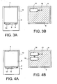
- FIG. 3A represents a view in section of the component and FIG. 3B represents a view top of the component, anode side.
- the component according to the first variant of the invention comprises a block of semiconductor material 6, for example a block of CdZnTe, covered on a first face of a cathode 7 and on a second face, opposite to the first face, anode 8.
- the anode 8 is covered with a thin substrate 9 in which is implanted an ASIC circuit 14.
- the ASIC circuit 14 is, for example, a circuit integrated system comprising a preamplifier, a amplifier and an analog / digital converter.
- a pad 12 collects the signal from the detector 6.
- the different elements that make up the component are gathered in a housing 15 with an opening leaving the cathode exposed to radiation.
- the amplifier contained in the ASIC 14 can advantageously comprise a circuit of electronic processing to improve the detection efficiency such as the described circuit in French Patent No. 2,738,919 filed in France on September 15, 1995 and entitled “Method and device for the correction of spectrometric measurements ".
- Figures 4A-4B represent a second component variant for spectrometric detection according to the invention.
- the component according to the second example of the invention comprises a second ASIC circuit 16.
- the ASIC 16 circuit is a high power circuit voltage that allows to apply an electric field in the semiconductor material.
- the ASIC circuit 16 is realized in silicon on insulator technology commonly called SOI technology (SOI for "Silicon On Insulator "), which allows you to perform a power supply with bias voltages of the order of a few hundred volts.
- SOI Silicon On Insulator
- the ASIC circuit 16 is implanted in the substrate 9, for example in silicon.
- Figures 5A-5B represent a third component variant for spectrometric detection according to the invention.
- the component according to the third variant of the invention comprises a third ASIC 17.
- the ASIC circuit 17 allows, for example, a electromagnetic transmission of detected data to circuits upstream of the chain of processing, for example receiving circuits placed in a personal computer. Any connection electrical cable between the detector and the computer personnel is then advantageously suppressed.
- Figure 6 shows a refinement of the first component variant according to the invention.
- the component according to enhancement includes a low power supply 18.
- the block 18 is made of strong batteries capacity to supply 0 / + 5 volts to the ASIC circuit 14. Block 18 is fixed, for example by gluing, to closer to the ASIC 14. It is then placed as this is represented in FIG. 6, on the wall of the housing that faces the anode of the detector.
- the component according to the invention comprises one or more elements ASIC and / or block type integration Power.
- the number of integration elements depends on the desired integration level. In any case, the integration of ASIC 14 is essential to optimize the performance of the detector.
- FIG. 7 represents a single-channel probe according to the invention.
- a source of gamma radiation 19 illuminates four detectors according to the invention D1, D2, D3, D4.
- the transmitted data are collected by a receiver unit 20 and displayed on a screen 21.
- the single channel probe is advantageously integrated in a few cm 3 without any electrical connection.
- a 2D imager 22 comprising a set of detection systems elementary 23 gathered together is represented in figure 8.
Landscapes
- Physics & Mathematics (AREA)
- Health & Medical Sciences (AREA)
- Life Sciences & Earth Sciences (AREA)
- General Physics & Mathematics (AREA)
- High Energy & Nuclear Physics (AREA)
- Molecular Biology (AREA)
- Spectroscopy & Molecular Physics (AREA)
- Measurement Of Radiation (AREA)
- Nuclear Medicine (AREA)
Abstract
Description
- une conversion directe du rayonnement en signal électrique plutôt qu'une conversion indirecte photons gamma/lumière/charges électriques obtenue par l'association d'un scintillateur et d'un photomultiplicateur,
- un fonctionnement à température ambiante qui permet de concevoir des détecteurs légers et compacts,
- des signaux électriques détectés d'amplitudes élevées permettant d'obtenir d'excellentes résolutions en énergie,
- la possibilité d'utiliser des détecteurs épais et de pouvoir disposer ces détecteurs matriciellement pour plus de sensibilité.
- un porte détecteur permettant de maintenir le détecteur à l'obscurité et d'isoler celui-ci des perturbations électromagnétiques,
- un préamplificateur de charge permettant d'intégrer le signal électrique généré par le semi-conducteur,
- une alimentation basse tension du préamplificateur,
- une alimentation haute tension afin d'appliquer un champ électrique au détecteur,
- un amplificateur permettant d'amplifier, filtrer et traiter les signaux électriques issus du préamplificateur,
- une alimentation basse tension de l'amplificateur,
- un convertisseur analogique digital (CAD) permettant de numériser les signaux électriques,
- une alimentation basse tension du convertisseur,
- un analyseur de spectre,
- un afficheur de type PC (PC pour « Personal Computer ») ou compteur.
- de réaliser facilement différentes dimensions d'imageur 2D avec différentes géométries de détecteurs et de pas associés,
- d'optimiser les performances du système en limitant au minimum la liaison électrique entre le détecteur et le préamplificateur,
- de pouvoir optimiser les performances des imageurs 2D en permettant d'associer une chaíne de spectrométrie par détecteur afin d'améliorer le taux de comptage.
- la figure 1 représente un système de détection spectrométrique selon l'art connu ;
- la figure 2 représente un exemple de réalisation du système de détection spectrométrique selon l'invention ;
- les figures 3A-3B représentent une première variante de composant pour la détection spectrométrique selon l'invention ;
- les figures 4A-4B représentent une deuxième variante de composant pour la détection spectrométrique selon l'invention ;
- les figures 5A-5B représentent une troisième variante de composant pour la détection spectrométrique selon l'invention ;
- la figure 6 représente un perfectionnement du composant selon la première variante de l'invention ;
- la figure 7 représente une sonde monovoie selon l'invention ;
- la figure 8 représente un imageur 2D selon l'invention.
Claims (11)
- Système de détection spectrométrique comprenant un bloc (6) de matériau semi-conducteur, une cathode (7) fixée sur une première face du bloc de matériau semi-conducteur et une anode (8) fixée sur une deuxième face du bloc de matériau semi-conducteur, les première et deuxième faces étant à l'opposé l'une de l'autre, caractérisé en ce qu'il comprend un substrat (9) fixé sur l'anode (8) et au moins un circuit ASIC (14) implanté dans le substrat, le circuit ASIC (14) comprenant une électronique de traitement d'un signal issu du bloc de matériau semi-conducteur.
- Système de détection spectrométrique selon la revendication 1, caractérisé en ce que le circuit ASIC (14) comprend un préamplificateur et un amplificateur pour respectivement pré-amplifier et amplifier le signal issu du bloc (6) de matériau semi-conducteur.
- Système de détection spectrométrique selon la revendication 2, caractérisé en ce que le circuit ASIC (14) comprend en outre un convertisseur analogique/digital pour convertir le signal issu de l'amplificateur en données numériques.
- Système de détection spectrométrique selon la revendication 3, caractérisé en ce qu'il comprend en outre, fixé sur le substrat (9), un circuit ASIC (17) pour la transmission électromagnétique des données numériques.
- Système de détection spectrométrique selon l'une quelconque des revendications 1 à 4, caractérisé en ce qu'il comprend en outre un circuit ASIC d'alimentation haute tension (16) implanté dans le substrat (9), pour appliquer un champ électrique dans le matériau semi-conducteur.
- Système de détection spectrométrique selon la revendication 5, caractérisé en ce que le circuit ASIC d'alimentation haute tension (16) est réalisé en technologie SOI.
- Système de détection spectrométrique selon l'une quelconque des revendications précédentes, caractérisé en ce qu'il comprend en outre un bloc d'alimentation basse tension (18).
- Système de détection spectrométrique selon l'une quelconque des revendications précédentes, caractérisé en ce qu'il est intégré dans un boítier (15).
- Système de détection spectrométrique selon la revendication 8, caractérisé en ce que le bloc d'alimentation basse tension (18) est fixé sur une face du boítier située à proximité de l'anode (8).
- Sonde monovoie, caractérisée en ce qu'elle comprend au moins un système de détection spectrométrique selon l'une quelconque des revendications 1 à 9.
- Imageur 2D, caractérisé en ce qu'il comprend une pluralité de système de détection spectrométriques selon l'une quelconque des revendications 1 à 9.
Applications Claiming Priority (2)
| Application Number | Priority Date | Filing Date | Title |
|---|---|---|---|
| FR0116550 | 2001-12-20 | ||
| FR0116550A FR2834073B1 (fr) | 2001-12-20 | 2001-12-20 | Systeme de detection spectrometrique integre a semi-conducteur |
Publications (1)
| Publication Number | Publication Date |
|---|---|
| EP1324074A1 true EP1324074A1 (fr) | 2003-07-02 |
Family
ID=8870747
Family Applications (1)
| Application Number | Title | Priority Date | Filing Date |
|---|---|---|---|
| EP02293143A Withdrawn EP1324074A1 (fr) | 2001-12-20 | 2002-12-18 | Système de détection spectrométrique intégré à semi-conducteur |
Country Status (3)
| Country | Link |
|---|---|
| US (1) | US20030150995A1 (fr) |
| EP (1) | EP1324074A1 (fr) |
| FR (1) | FR2834073B1 (fr) |
Citations (1)
| Publication number | Priority date | Publication date | Assignee | Title |
|---|---|---|---|---|
| EP1067403A1 (fr) * | 1999-07-08 | 2001-01-10 | Commissariat A L'energie Atomique | Matrice de détecteurs de photons |
Family Cites Families (10)
| Publication number | Priority date | Publication date | Assignee | Title |
|---|---|---|---|---|
| FR2757685B1 (fr) * | 1996-12-24 | 1999-05-14 | Commissariat Energie Atomique | Dispositif de detection de rayonnements ionisants a semi-conducteur de haute resistivite |
| EP1116047B1 (fr) * | 1998-09-24 | 2006-07-12 | Elgems Ltd. | Detecteur photoelectrique pixelise |
| FR2793072B1 (fr) * | 1999-04-30 | 2001-11-30 | Commissariat Energie Atomique | Dispositif de detection compact pour gamma camera |
| FR2793071B1 (fr) * | 1999-04-30 | 2001-06-08 | Commissariat Energie Atomique | Gamma camera miniature a detecteurs semiconducteurs |
| US6573762B1 (en) * | 1999-11-05 | 2003-06-03 | Sandia Corporation | Analog pulse processor |
| US6472748B1 (en) * | 2000-03-06 | 2002-10-29 | Harris Broadband Wireless Access, Inc. | System and method for providing MMIC seal |
| IL137579A (en) * | 2000-07-30 | 2006-12-31 | Orbotech Medical Solutions Ltd | Gamma-ray detector for coincidence detection |
| JP2002052015A (ja) * | 2000-08-07 | 2002-02-19 | Shimadzu Corp | 平面型放射線検出器ユニット及びx線撮像装置 |
| US6940071B2 (en) * | 2000-10-11 | 2005-09-06 | University Of Southampton | Gamma-ray spectrometry |
| US6730914B2 (en) * | 2002-02-05 | 2004-05-04 | E-Phocus, Inc. | Photoconductor-on-active-pixel (POAP) sensor utilizing equal-potential pixel electrodes |
-
2001
- 2001-12-20 FR FR0116550A patent/FR2834073B1/fr not_active Expired - Fee Related
-
2002
- 2002-12-18 EP EP02293143A patent/EP1324074A1/fr not_active Withdrawn
- 2002-12-20 US US10/327,703 patent/US20030150995A1/en not_active Abandoned
Patent Citations (1)
| Publication number | Priority date | Publication date | Assignee | Title |
|---|---|---|---|---|
| EP1067403A1 (fr) * | 1999-07-08 | 2001-01-10 | Commissariat A L'energie Atomique | Matrice de détecteurs de photons |
Also Published As
| Publication number | Publication date |
|---|---|
| US20030150995A1 (en) | 2003-08-14 |
| FR2834073A1 (fr) | 2003-06-27 |
| FR2834073B1 (fr) | 2004-02-13 |
Similar Documents
| Publication | Publication Date | Title |
|---|---|---|
| US5500534A (en) | Integrated energy-sensitive and position-sensitive x-ray detection system | |
| Mackay | Charge-coupled devices in astronomy | |
| US5440130A (en) | X-ray imaging system and solid state detector therefor | |
| US7872218B2 (en) | Radiation image pickup apparatus and its control method | |
| US7791034B2 (en) | Imaging apparatus, radiation imaging apparatus, and radiation imaging system | |
| EP1540730B1 (fr) | Dispositif d'imagerie de rayonnement de comptage par impulsion/photon de pixel de detecteur jumele | |
| Hu et al. | A large-scale multimodal CMOS biosensor array with 131,072 pixels and code-division multiplexed readout | |
| Zandian et al. | Performance of science grade HgCdTe H4RG-15 image sensors | |
| Andricek et al. | DePFET—Recent developments and future prospects | |
| US20060077269A1 (en) | Pixel binning image sensor | |
| EP1156347A1 (fr) | Dispositif porte-détecteur pour la détection de rayonnements ionisants | |
| Oonuki et al. | Development of uniform CdTe pixel detectors based on Caltech ASIC | |
| EP1049170A1 (fr) | Gamma caméra miniature a détecteurs semi-conducteurs | |
| EP1324074A1 (fr) | Système de détection spectrométrique intégré à semi-conducteur | |
| Treberspurg et al. | Performance of a kilo-pixel RNDR-DEPFET detector | |
| EP1188187A1 (fr) | Detecteur a semi-conducteur pour la detection de rayonnements ionisants | |
| CN118749075A (zh) | 辐射探测器和探测方法 | |
| Finger et al. | Performance evaluation and calibration issues of large format infrared hybrid active pixel sensors used for ground-and space-based astronomy | |
| Sanjeevi et al. | Next generation CMOS TDI detectors | |
| US6891489B2 (en) | Cross-talk linearity connection | |
| Miyasaka et al. | Development of a cadmium telluride pixel detector for astrophysical applications | |
| FR2713037A1 (fr) | Circuit d'injection, en imagerie thermique. | |
| Treis et al. | The wide field imager for the International X-ray Observatory | |
| Hartmann et al. | Results of a pnCCD detector system for high-speed optical imaging | |
| Adkins | Review of the latest developments in fast low noise detectors for wavefront sensing in the visible |
Legal Events
| Date | Code | Title | Description |
|---|---|---|---|
| PUAI | Public reference made under article 153(3) epc to a published international application that has entered the european phase |
Free format text: ORIGINAL CODE: 0009012 |
|
| AK | Designated contracting states |
Designated state(s): AT BE BG CH CY CZ DE DK EE ES FI FR GB GR IE IT LI LU MC NL PT SE SI SK TR |
|
| AX | Request for extension of the european patent |
Extension state: AL LT LV MK RO |
|
| 17P | Request for examination filed |
Effective date: 20031217 |
|
| AKX | Designation fees paid |
Designated state(s): AT BE BG CH CY CZ DE DK EE ES FI FR GB GR IE IT LI LU MC NL PT SE SI SK TR |
|
| RAP1 | Party data changed (applicant data changed or rights of an application transferred) |
Owner name: COMMISSARIAT A L'ENERGIE ATOMIQUE |
|
| 17Q | First examination report despatched |
Effective date: 20100224 |
|
| RAP1 | Party data changed (applicant data changed or rights of an application transferred) |
Owner name: COMMISSARIAT A L'ENERGIE ATOMIQUE ET AUX ENERGIES |
|
| STAA | Information on the status of an ep patent application or granted ep patent |
Free format text: STATUS: THE APPLICATION IS DEEMED TO BE WITHDRAWN |
|
| 18D | Application deemed to be withdrawn |
Effective date: 20120703 |