EP1324072A2 - Distance measuring device - Google Patents
Distance measuring device Download PDFInfo
- Publication number
- EP1324072A2 EP1324072A2 EP02027925A EP02027925A EP1324072A2 EP 1324072 A2 EP1324072 A2 EP 1324072A2 EP 02027925 A EP02027925 A EP 02027925A EP 02027925 A EP02027925 A EP 02027925A EP 1324072 A2 EP1324072 A2 EP 1324072A2
- Authority
- EP
- European Patent Office
- Prior art keywords
- signal
- measuring device
- distance measuring
- rit
- circuit
- Prior art date
- Legal status (The legal status is an assumption and is not a legal conclusion. Google has not performed a legal analysis and makes no representation as to the accuracy of the status listed.)
- Granted
Links
Images


Classifications
-
- G—PHYSICS
- G01—MEASURING; TESTING
- G01S—RADIO DIRECTION-FINDING; RADIO NAVIGATION; DETERMINING DISTANCE OR VELOCITY BY USE OF RADIO WAVES; LOCATING OR PRESENCE-DETECTING BY USE OF THE REFLECTION OR RERADIATION OF RADIO WAVES; ANALOGOUS ARRANGEMENTS USING OTHER WAVES
- G01S7/00—Details of systems according to groups G01S13/00, G01S15/00, G01S17/00
- G01S7/48—Details of systems according to groups G01S13/00, G01S15/00, G01S17/00 of systems according to group G01S17/00
- G01S7/497—Means for monitoring or calibrating
-
- G—PHYSICS
- G01—MEASURING; TESTING
- G01S—RADIO DIRECTION-FINDING; RADIO NAVIGATION; DETERMINING DISTANCE OR VELOCITY BY USE OF RADIO WAVES; LOCATING OR PRESENCE-DETECTING BY USE OF THE REFLECTION OR RERADIATION OF RADIO WAVES; ANALOGOUS ARRANGEMENTS USING OTHER WAVES
- G01S17/00—Systems using the reflection or reradiation of electromagnetic waves other than radio waves, e.g. lidar systems
- G01S17/02—Systems using the reflection of electromagnetic waves other than radio waves
- G01S17/06—Systems determining position data of a target
- G01S17/08—Systems determining position data of a target for measuring distance only
- G01S17/10—Systems determining position data of a target for measuring distance only using transmission of interrupted, pulse-modulated waves
- G01S17/14—Systems determining position data of a target for measuring distance only using transmission of interrupted, pulse-modulated waves wherein a voltage or current pulse is initiated and terminated in accordance with the pulse transmission and echo reception respectively, e.g. using counters
-
- G—PHYSICS
- G01—MEASURING; TESTING
- G01S—RADIO DIRECTION-FINDING; RADIO NAVIGATION; DETERMINING DISTANCE OR VELOCITY BY USE OF RADIO WAVES; LOCATING OR PRESENCE-DETECTING BY USE OF THE REFLECTION OR RERADIATION OF RADIO WAVES; ANALOGOUS ARRANGEMENTS USING OTHER WAVES
- G01S7/00—Details of systems according to groups G01S13/00, G01S15/00, G01S17/00
- G01S7/48—Details of systems according to groups G01S13/00, G01S15/00, G01S17/00 of systems according to group G01S17/00
- G01S7/483—Details of pulse systems
- G01S7/486—Receivers
- G01S7/4865—Time delay measurement, e.g. time-of-flight measurement, time of arrival measurement or determining the exact position of a peak
-
- G—PHYSICS
- G01—MEASURING; TESTING
- G01S—RADIO DIRECTION-FINDING; RADIO NAVIGATION; DETERMINING DISTANCE OR VELOCITY BY USE OF RADIO WAVES; LOCATING OR PRESENCE-DETECTING BY USE OF THE REFLECTION OR RERADIATION OF RADIO WAVES; ANALOGOUS ARRANGEMENTS USING OTHER WAVES
- G01S7/00—Details of systems according to groups G01S13/00, G01S15/00, G01S17/00
- G01S7/48—Details of systems according to groups G01S13/00, G01S15/00, G01S17/00 of systems according to group G01S17/00
- G01S7/483—Details of pulse systems
- G01S7/486—Receivers
- G01S7/487—Extracting wanted echo signals, e.g. pulse detection
Definitions
- the present invention relates to a distance measuring device.
- the present invention relates to an optoelectronic distance measuring device of the type comprising a light emitting unit having, for example, a LASER photoemitter for generating a light beam defined by a number of light pulses in a predetermined direction; an optical assembly for focusing and deflecting the light beam generated by the photoemitter, so as to "channel” it onto an object whose distance with respect to the distance measuring device is to be measured; and a light receiving unit for picking up and converting the light beam reflected by the object into an electric signal, the voltage or current value to time pattern of which is related to the distance between the object and the distance measuring device.
- a light emitting unit having, for example, a LASER photoemitter for generating a light beam defined by a number of light pulses in a predetermined direction
- an optical assembly for focusing and deflecting the light beam generated by the photoemitter, so as to "channel” it onto an object whose distance with respect to the distance measuring device is to be measured
- the receiving unit normally comprises a photoreceiver for converting the light pulses of the reflected beam into electric pulses, each of which has a delay (with respect to the emitted pulse) related to the distance travelled by the light pulse to and from the object; and an amplifying circuit for maintaining a substantially constant amplitude of each received electric pulse, regardless of the distance and reflectance of the object.
- the receiving unit also comprises a processing circuit for receiving and so processing the electric pulses from the amplifying circuit as to supply a signal indicating the measured distance. More specifically, the processing circuit determines the measured-distance signal as a function of the "transit time", i.e. by processing the delay, of each received electric pulse.
- the measurement supplied by known distance measuring devices of the type described is affected by errors related to the circuit propagation delays introduced into the electric pulses during processing by the electronic circuits in the receiving unit.
- Which propagation delays vary as a function of changes in the circuit parameter values of the electric components, caused, for example, by variations in the temperature to which the electronic circuits are subjected, and/or by ageing of the electronic circuits.
- the duration of the electric pulse generated during processing is related both to the "transit time” taken by the beam to travel the "net” distance between the object and the distance measuring device, and to the internal propagation delays of the circuits.
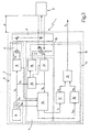
- Figure 1 shows a block diagram of a distance measuring device in accordance with the teachings of the present invention
- Figure 2 shows a time graph of a number of signals generated by electric circuits forming part of the distance measuring device in Figure 1;
- Figure 3 shows a block diagram of a variation of the distance measuring device in Figure 1;
- Figure 4 shows a time graph of a number of signals generated by electric circuits forming part of the distance measuring device in Figure 3.
- Number 1 in Figure 1 indicates as a whole an optoelectronic distance measuring device for measuring the distance D of a generic object 2 with respect to distance measuring device 1.
- Distance measuring device 1 comprises an emitting unit 3 for generating a light beam onto object 2; an optical assembly 4 for focusing and deflecting the light beam, so as to "channel” it to and from object 2; and a receiving unit 5 for receiving and converting the light beam reflected by object 2 into an electric signal S R related to the distance D of object 2 from distance measuring device 1, and for so processing electric signal S R as to supply a distance signal S D indicating the measured distance D.
- optical assembly 4 comprises a number of lenses and mirrors (and any interference and polarizing filters not shown) appropriately arranged at emitting unit 3 to orient the generated light beam onto object 2, and at receiving unit 5 to "channel" the light beam reflected by object 2 towards receiving unit 5.
- Optical assembly 4 is a known type and therefore not described in detail.
- Emitting unit 3 comprises a photoemitter 6 for emitting the light beam onto object 2; and a signal generating circuit 7 for controlling photoemitter 6, and in turn comprising a clock generator 8 for supplying a clock signal S K , and a modulating circuit 9 for controlling, as a function of clock signal S K , emission of the light beam by photoemitter 6.
- Clock generator 8 may be defined by a quartz generator for supplying clock signal S K (e.g. a rectangular wave) with a predetermined ratio between the duration T ON of its pulses and its period T (duty cycle, for example, of 50%). If distance measuring device 1 comprises a microprocessor (not shown), clock signal S K may obviously be supplied directly by the microprocessor itself.
- clock signal S K e.g. a rectangular wave
- Modulating circuit 9 may be defined by a modulator for generating, as a function of clock signal S K , a control signal S C defined by a number of equally spaced electric pulses of predetermined amplitude and duration.
- each electric pulse of control signal S C is generated by modulating circuit 9 at each leading edge of clock signal S K , and has a very short duration, i.e. in the order, for example, of a few nanoseconds.
- Modulating circuit 9 also generates, as a function of clock signal S K , a reference signal S RIF defined by a number of equally spaced electric pulses of predetermined amplitude and duration.
- each electric pulse of reference signal S RIF is generated by modulating circuit 9 at each trailing edge of clock signal S K , and has a very short duration, i.e. in the order of a few nanoseconds.
- photoemitter 6 may be defined, for example, by a laser diode operating, preferably but not necessarily, in the infrared range, and which receives control signal S C from modulating circuit 9, and generates, as a function of control signal S C , a light beam defined by a number of light pulses, each of predetermined amplitude and duration.
- each light pulse hereinafter indicated I EM , is generated by emitting unit 3 at each leading edge of the pulses in control signal S C .
- receiving unit 5 comprises a photoreceiver 10 for picking up and converting the light pulses I EM in the light beam reflected by object 2 into signal S R comprising a series of electric pulses, each of which has a leading edge spaced by a time interval T OF with respect to the leading edge of the respective light pulses I EM emitted by photoemitter 6.
- time interval T OF is commonly referred to as "transit time”, and is related to the length of the optical path between emitting unit 3, object 2, and receiving unit 5.
- the "net” optical distance D is a fraction of said optical path, which is twice "net” optical distance D plus the optical paths within distance measuring device 1.
- Receiving unit 5 also comprises a processing circuit 11 for processing the pulses of signal S R from photoreceiver 10, and in turn supplying a pulse signal S T (shown in Figure 2) defined by a sequence of pulses I T , each having a duration ⁇ T related both to transit time T OF and to the internal circuit delays ⁇ RIT introduced by processing circuit 11 during processing.
- a processing circuit 11 for processing the pulses of signal S R from photoreceiver 10, and in turn supplying a pulse signal S T (shown in Figure 2) defined by a sequence of pulses I T , each having a duration ⁇ T related both to transit time T OF and to the internal circuit delays ⁇ RIT introduced by processing circuit 11 during processing.
- Processing circuit 11 also cooperates with signal generating circuit 7, from which it receives reference signal S RIF , and generates, as a function of reference signal S RIF , a delay signal S RIT (shown in Figure 2) whose duration is related to the internal circuit delays ⁇ RIT introduced into pulses I T of pulse signal S T by processing circuit 11 when processing the electric pulses of signal S R .
- signal generating circuit 7 receives reference signal S RIF , and generates, as a function of reference signal S RIF , a delay signal S RIT (shown in Figure 2) whose duration is related to the internal circuit delays ⁇ RIT introduced into pulses I T of pulse signal S T by processing circuit 11 when processing the electric pulses of signal S R .
- Receiving unit 5 also comprises a filtering and matching circuit 12, which processes delay signal S RIT and pulse signal S T to eliminate from pulse signal S T all the internal circuit delays ⁇ RIT introduced by processing circuit 11 when processing the electric pulses of signal S R , and so supply distance signal S D indicating the measured net distance D.
- a filtering and matching circuit 12 which processes delay signal S RIT and pulse signal S T to eliminate from pulse signal S T all the internal circuit delays ⁇ RIT introduced by processing circuit 11 when processing the electric pulses of signal S R , and so supply distance signal S D indicating the measured net distance D.
- photoreceiver 10 may be defined, for example, by an avalanche photodiode (APD) connected to a predetermined load, while processing circuit 11 comprises an amplifying circuit 13, which sequentially receives the electric pulses of signal S R from photoreceiver 10, and the electric pulses of reference signal S RIF from modulating circuit 9, and supplies a signal S A defined by superimposing and appropriately amplifying the pulses of signals S R and S RIF .
- the signal S A supplied by amplifying circuit 13 therefore comprises a sequence of alternating, appropriately amplified pulses P 1 and P 2 as shown in Figure 2.
- Processing circuit 11 also comprises a supply circuit 14 for supplying photoreceiver 10 with a predetermined supply voltage; and an amplitude detecting circuit 15, which, as a function of signal S A amplified by amplifying circuit 13, controls both supply circuit 14, to appropriately regulate the voltage supply (and therefore gain) of photoreceiver 10, and amplifying circuit 13, to maintain a predetermined amplitude of the electric pulses of signal S R supplied by amplifying circuit 13, regardless of distance D and the reflectance of object 2.
- amplitude detecting circuit 15 receives clock signal S K from clock generator 8 to control, together with amplifying circuit 13 and supply circuit 14, amplification of the electric pulses of signal S R . It should be pointed out that detecting circuit 15, by acting on supply circuit 14, varies the amplitude of each electric pulse in signal S R , while leaving the amplitude of the electric pulses in reference signal S RIF unchanged.
- the amplitudes of pulses P 1 and P 2 in signal S A can be equalized by appropriately varying supply to photoreceiver 10 (i.e. by varying the reverse voltage supplied to the APD). That is, the amplification of pulses P 1 of the received optical signal can be varied, while at the same time maintaining constant amplification of pulses P 2 of reference signal S RIF .
- processing circuit 11 also comprises a pulse shaping and separating circuit 16 for receiving and processing electric pulses P 1 and P 2 of signal S A from amplifying circuit 13, and clock signal S K from clock generator 8, so as to supply, at a first output, pulse signal S T defined by pulses I T having duration ⁇ T related both to "transit time” T OF of the relative pulses picked up by photoreceiver 10, and to the circuit delays ⁇ RIT introduced by processing circuit 11.
- pulse shaping and separating circuit 16 for receiving and processing electric pulses P 1 and P 2 of signal S A from amplifying circuit 13, and clock signal S K from clock generator 8, so as to supply, at a first output, pulse signal S T defined by pulses I T having duration ⁇ T related both to "transit time" T OF of the relative pulses picked up by photoreceiver 10, and to the circuit delays ⁇ RIT introduced by processing circuit 11.
- Pulse shaping circuit 16 also supplies, at a second output, delay signal S RIT comprising electric pulses I RIT , each of a duration ⁇ RIT related to the circuit delays introduced into pulse signal S T by the electronic components (not shown) of photoreceiver 10, amplifying circuit 13, and pulse shaping circuit 16 itself.
- pulse signal S T has a leading edge corresponding with the leading edge of the emitted light pulse I EM , and a trailing edge corresponding with a predetermined (e.g. mid-amplitude) point on the leading edge of pulse P 1 of signal S A ; whereas each pulse in delay signal S RIT has a leading edge corresponding with the leading edge of a pulse in reference signal S RIF , and a trailing edge corresponding with a predetermined (e.g. mid-amplitude) point on the leading edge of pulse P 2 of signal S A .
- a predetermined e.g. mid-amplitude
- filtering circuit 12 comprises a filter 17 for receiving pulse signal S T from pulse shaping circuit 16, and producing, by means of a given transfer function, a voltage signal V T having an amplitude proportional to the duration ⁇ T of each electric pulse I T of pulse signal S T .
- Filtering circuit 12 also comprises a filter 18 for receiving delay signal S RIT from pulse shaping circuit 16, and producing, by means of a given transfer function, a voltage signal V RIT having an amplitude proportional to the duration ⁇ RIT of each electric pulse I RIT of delay signal S RIT .
- filtering circuit 12 also comprises a calculating circuit 19 for receiving and processing signals V RIT and V T from respective filters 18 and 17, to eliminate the contribution of the circuit delays in signal V T . More specifically, calculating circuit 19 implements a predetermined transfer function F 1 for calculating the difference between signal V T and signal V RIT , so as to obtain a distance signal S D from which any error caused by delays introduced by processing circuit 11 is "filtered".
- G is the gain of the calculating circuit
- V o is a reference signal of a predetermined voltage.
- transfer function F 1 i.e. by varying gain G and signal V o
- calculating circuit 19 is able to adapt distance signal S D indicating distance D to the requirements of the user.
- the operations performed by calculating circuit 19 by means of transfer function F 1 may obviously be performed by means of an appropriate analog circuit (defined by operational amplifiers), or by means of a microprocessor with predetermined software, by which to implement transfer function F 1 to obtain distance signal S D from signals V REF and V T .
- distance measuring device 1 Operation of distance measuring device 1 is easily deducible from the foregoing description with no further explanation required.
- Distance measuring device 1 as described above has the advantage of greatly improving distance measuring accuracy as compared with known devices, by eliminating any distance measuring errors caused by alteration of the distance signals by circuit delays introduced by internal electric circuits (as a result, for example, of a change in temperature).
- the distance measuring device in the Figure 3 variation differs from distance measuring device 1 described above by the reference signal S RIF generated by signal generating circuit 7 being supplied directly to pulse shaping circuit 16 of processing circuit 11, as opposed to going through amplifying circuit 13.
- distance measuring device 1 in Figure 3 is able to eliminate the internal circuit delays introduced into pulse signal S T by pulse shaping circuit 16 when processing signal S A .
- Pulse shaping circuit 16 receives clock signal S K and reference signal S RIF from clock generator 8, and signal S A from amplifying circuit 13, and processes these signals to generate delay signal S RIT and pulse signal S T at two different outputs.
- the leading edges of the pulses in delay signal S RIT and pulse signal S T are generated by pulse shaping circuit 16 at the leading edge of reference signal S RIF , while the trailing edge of each pulse I T of pulse signal S T is generated at a predetermined (e.g. mid-amplitude) point T 1 of the leading edge of signal S A .
- each pulse I RIT in delay signal S RIT is generated at the leading edge of pulse I EM .
- the duration of signal S T also comprises a predetermined lead time interval ⁇ ANT corresponding to the time interval between the leading edge of the pulse of reference signal S RIF and the leading edge of the pulse of clock signal S K .
- lead time interval ⁇ ANT is introduced to compensate for overshooting in pulse signal S T when shaping each pulse I T , and in delay signal S RIT when shaping each pules I RIT .
- said circuit delays ⁇ TA and ⁇ TB in pulse I T are also introduced equally by pulse shaping circuit 16 at the leading edge and trailing edge respectively of pulse I RIT of delay signal S RIT .
- Delay signal S RIT therefore has a duration ⁇ RIT related both to the circuit delays introduced into pulse signal S T by pulse shaping circuit 16, and to the lead time interval ⁇ ANT introduced, as stated, to compensate for switching-generated overshooting and oscillations in pulse signal S T and delay signal S RIT .
- pulse shaping circuit 16 may be provided with digital electronic circuits (not shown), e.g. a first and a second flip-flop integrated in the same chip so as to have the same performance in terms of signal response time to variations in characteristics resulting from thermal drift and ageing.
- the first flip-flop (not shown) generates pulse signal S T at the leading edge of reference signal S RIF and the predetermined point on the leading edge of signal S A
- the second flip-flop (not shown) generates delay signal S RIT as a function of the leading edges of the pulses of reference signal S RIF and the leading edges of the pulses of signal I EM respectively.
- pulse shaping circuit 16 in use, the two digital circuits (first and second flip-flop) integrated in pulse shaping circuit 16 are subjected at all times to the same operating temperature (by forming part of the same chip), and, by having the same dynamic behaviour, advantageously introduce into each pulse I T and I RIT the same variations in circuit delays ⁇ TA and ⁇ TB , regardless of the operating temperature of the circuit.
- pulse shaping circuit 16 regardless of its thermal condition, pulse shaping circuit 16 generates a delay signal S RIT containing both information relative to internal circuit delays ⁇ TA and ⁇ TB affecting pulse signal S T , and information relating to predetermined lead time interval ⁇ ANT .
- Delay signal S RIT and pulse signal S T are supplied by pulse shaping circuit 16 to filtering and matching circuit 12, which, by means of filters 17 and 18, generates voltage signals V T and V RIT having an amplitude proportional to duration ⁇ T and ⁇ RIT respectively of each electric pulse I T and I RIT .
- filtering circuit 12 is also able to determine distance signal S D as a function of signals V T and V RIT by means of a predetermined transfer function for eliminating from signal V T , associated with pulse signal S T , both the component relative to the internal circuit delays of pulse shaping circuit 16 indicated by delay signal S RIT , and the predetermined lead time interval ⁇ ANT .
- signal V T associated with pulse signal S T may, for example, be calculated by means of a function for determining the mean value of a series of pulses I T of pulse signal S T . More specifically, in calculating the mean value, the "leading" overshoot and oscillation (indicated E A in the Figure 4 example) present in the leading edge of each pulse I T and completely smoothed out by lead time interval ⁇ ANT is compensated with the "trailing" overshoot and oscillation (indicated E B in the Figure 4 example) generated at the trailing edge of each pulse I T , thus advantageously eliminating the measuring error in pulse signal S T , and consequently in distance signal S D , introduced by overshooting and oscillation in both pulse signal S T and delay signal S RIT .
- distance measuring device 1 may supply reference signal S RIF optically to processing circuit 11 along an internal optical reference path (e.g. by means of an optical fibre).
- distance measuring device 1 may comprise an internal optical reference path of predetermined length, by which a reference light pulse is sent by photoemitter 6 (controlled by signal generating circuit 7) to photoreceiver 10.
- photoreceiver 10 By converting the reference light pulse into an electric signal, photoreceiver 10 supplies reference signal S RIF to processing circuit 11, which in turn generates delay signal S RIT .
Landscapes
- Engineering & Computer Science (AREA)
- Physics & Mathematics (AREA)
- Computer Networks & Wireless Communication (AREA)
- General Physics & Mathematics (AREA)
- Radar, Positioning & Navigation (AREA)
- Remote Sensing (AREA)
- Electromagnetism (AREA)
- Optical Radar Systems And Details Thereof (AREA)
- Measurement Of Optical Distance (AREA)
- Radar Systems Or Details Thereof (AREA)
- Telephone Function (AREA)
- Credit Cards Or The Like (AREA)
Abstract
Description
- The present invention relates to a distance measuring device.
- More specifically, the present invention relates to an optoelectronic distance measuring device of the type comprising a light emitting unit having, for example, a LASER photoemitter for generating a light beam defined by a number of light pulses in a predetermined direction; an optical assembly for focusing and deflecting the light beam generated by the photoemitter, so as to "channel" it onto an object whose distance with respect to the distance measuring device is to be measured; and a light receiving unit for picking up and converting the light beam reflected by the object into an electric signal, the voltage or current value to time pattern of which is related to the distance between the object and the distance measuring device.
- In known distance measuring devices of the type described above, the receiving unit normally comprises a photoreceiver for converting the light pulses of the reflected beam into electric pulses, each of which has a delay (with respect to the emitted pulse) related to the distance travelled by the light pulse to and from the object; and an amplifying circuit for maintaining a substantially constant amplitude of each received electric pulse, regardless of the distance and reflectance of the object.
- The receiving unit also comprises a processing circuit for receiving and so processing the electric pulses from the amplifying circuit as to supply a signal indicating the measured distance. More specifically, the processing circuit determines the measured-distance signal as a function of the "transit time", i.e. by processing the delay, of each received electric pulse.
- Known distance measuring devices of the above type have the major drawback of failing to provide for accurate distance measurements.
- That is, the measurement supplied by known distance measuring devices of the type described is affected by errors related to the circuit propagation delays introduced into the electric pulses during processing by the electronic circuits in the receiving unit. Which propagation delays vary as a function of changes in the circuit parameter values of the electric components, caused, for example, by variations in the temperature to which the electronic circuits are subjected, and/or by ageing of the electronic circuits.
- More specifically, the duration of the electric pulse generated during processing is related both to the "transit time" taken by the beam to travel the "net" distance between the object and the distance measuring device, and to the internal propagation delays of the circuits.
- It is an object of the present invention to provide a distance measuring device of the type described above, designed to eliminate the aforementioned drawbacks.
- According to the present invention, there is provided a distance measuring device as claimed in Claim 1.
- A non-limiting embodiment of the present invention will be described by way of example with reference to the accompanying drawings, in which:
- Figure 1 shows a block diagram of a distance measuring device in accordance with the teachings of the present invention;
- Figure 2 shows a time graph of a number of signals generated by electric circuits forming part of the distance measuring device in Figure 1;
- Figure 3 shows a block diagram of a variation of the distance measuring device in Figure 1;
- Figure 4 shows a time graph of a number of signals generated by electric circuits forming part of the distance measuring device in Figure 3.
- Number 1 in Figure 1 indicates as a whole an optoelectronic distance measuring device for measuring the distance D of a generic object 2 with respect to distance measuring device 1.
- Distance measuring device 1 comprises an emitting unit 3 for generating a light beam onto object 2; an optical assembly 4 for focusing and deflecting the light beam, so as to "channel" it to and from object 2; and a receiving unit 5 for receiving and converting the light beam reflected by object 2 into an electric signal SR related to the distance D of object 2 from distance measuring device 1, and for so processing electric signal SR as to supply a distance signal SD indicating the measured distance D.
- In the example shown, optical assembly 4 comprises a number of lenses and mirrors (and any interference and polarizing filters not shown) appropriately arranged at emitting unit 3 to orient the generated light beam onto object 2, and at receiving unit 5 to "channel" the light beam reflected by object 2 towards receiving unit 5. Optical assembly 4 is a known type and therefore not described in detail.
- Emitting unit 3 comprises a photoemitter 6 for emitting the light beam onto object 2; and a signal generating circuit 7 for controlling photoemitter 6, and in turn comprising a clock generator 8 for supplying a clock signal SK, and a modulating circuit 9 for controlling, as a function of clock signal SK, emission of the light beam by photoemitter 6.
- Clock generator 8 may be defined by a quartz generator for supplying clock signal SK (e.g. a rectangular wave) with a predetermined ratio between the duration TON of its pulses and its period T (duty cycle, for example, of 50%). If distance measuring device 1 comprises a microprocessor (not shown), clock signal SK may obviously be supplied directly by the microprocessor itself.
- Modulating circuit 9 may be defined by a modulator for generating, as a function of clock signal SK, a control signal SC defined by a number of equally spaced electric pulses of predetermined amplitude and duration. In the Figure 2 example, each electric pulse of control signal SC is generated by modulating circuit 9 at each leading edge of clock signal SK, and has a very short duration, i.e. in the order, for example, of a few nanoseconds.
- Modulating circuit 9 also generates, as a function of clock signal SK, a reference signal SRIF defined by a number of equally spaced electric pulses of predetermined amplitude and duration. In the Figure 2 example, each electric pulse of reference signal SRIF is generated by modulating circuit 9 at each trailing edge of clock signal SK, and has a very short duration, i.e. in the order of a few nanoseconds.
- With reference to Figure 1, photoemitter 6 may be defined, for example, by a laser diode operating, preferably but not necessarily, in the infrared range, and which receives control signal SC from modulating circuit 9, and generates, as a function of control signal SC, a light beam defined by a number of light pulses, each of predetermined amplitude and duration. In the Figure 2 example, each light pulse, hereinafter indicated IEM, is generated by emitting unit 3 at each leading edge of the pulses in control signal SC.
- with reference to Figure 1, receiving unit 5 comprises a photoreceiver 10 for picking up and converting the light pulses IEM in the light beam reflected by object 2 into signal SR comprising a series of electric pulses, each of which has a leading edge spaced by a time interval TOF with respect to the leading edge of the respective light pulses IEM emitted by photoemitter 6.
- In the example shown, time interval TOF is commonly referred to as "transit time", and is related to the length of the optical path between emitting unit 3, object 2, and receiving unit 5.
- in connection with the above, it should be pointed out that the "net" optical distance D is a fraction of said optical path, which is twice "net" optical distance D plus the optical paths within distance measuring device 1.
- Receiving unit 5 also comprises a processing circuit 11 for processing the pulses of signal SR from photoreceiver 10, and in turn supplying a pulse signal ST (shown in Figure 2) defined by a sequence of pulses IT, each having a duration ΔT related both to transit time TOF and to the internal circuit delays ΔRIT introduced by processing circuit 11 during processing.
- Processing circuit 11 also cooperates with signal generating circuit 7, from which it receives reference signal SRIF, and generates, as a function of reference signal SRIF, a delay signal SRIT (shown in Figure 2) whose duration is related to the internal circuit delays ΔRIT introduced into pulses IT of pulse signal ST by processing circuit 11 when processing the electric pulses of signal SR.
- Receiving unit 5 also comprises a filtering and matching circuit 12, which processes delay signal SRIT and pulse signal ST to eliminate from pulse signal ST all the internal circuit delays ΔRIT introduced by processing circuit 11 when processing the electric pulses of signal SR, and so supply distance signal SD indicating the measured net distance D.
- With reference to Figure 1, photoreceiver 10 may be defined, for example, by an avalanche photodiode (APD) connected to a predetermined load, while processing circuit 11 comprises an amplifying circuit 13, which sequentially receives the electric pulses of signal SR from photoreceiver 10, and the electric pulses of reference signal SRIF from modulating circuit 9, and supplies a signal SA defined by superimposing and appropriately amplifying the pulses of signals SR and SRIF. The signal SA supplied by amplifying circuit 13 therefore comprises a sequence of alternating, appropriately amplified pulses P1 and P2 as shown in Figure 2.
- In connection with the above, it should be pointed out that the output of modulating circuit 9 supplying reference signal SRIF is connected electrically to the input of amplifying circuit 13 receiving signal SR.
- Processing circuit 11 also comprises a supply circuit 14 for supplying photoreceiver 10 with a predetermined supply voltage; and an amplitude detecting circuit 15, which, as a function of signal SA amplified by amplifying circuit 13, controls both supply circuit 14, to appropriately regulate the voltage supply (and therefore gain) of photoreceiver 10, and amplifying circuit 13, to maintain a predetermined amplitude of the electric pulses of signal SR supplied by amplifying circuit 13, regardless of distance D and the reflectance of object 2.
- More specifically, amplitude detecting circuit 15 receives clock signal SK from clock generator 8 to control, together with amplifying circuit 13 and supply circuit 14, amplification of the electric pulses of signal SR. It should be pointed out that detecting circuit 15, by acting on supply circuit 14, varies the amplitude of each electric pulse in signal SR, while leaving the amplitude of the electric pulses in reference signal SRIF unchanged.
- In the example shown, using an APD photoreceiver 10, the amplitudes of pulses P1 and P2 in signal SA can be equalized by appropriately varying supply to photoreceiver 10 (i.e. by varying the reverse voltage supplied to the APD). That is, the amplification of pulses P1 of the received optical signal can be varied, while at the same time maintaining constant amplification of pulses P2 of reference signal SRIF.
- With reference to Figure 1, processing circuit 11 also comprises a pulse shaping and separating circuit 16 for receiving and processing electric pulses P1 and P2 of signal SA from amplifying circuit 13, and clock signal SK from clock generator 8, so as to supply, at a first output, pulse signal ST defined by pulses IT having duration ΔT related both to "transit time" TOF of the relative pulses picked up by photoreceiver 10, and to the circuit delays ΔRIT introduced by processing circuit 11.
- Pulse shaping circuit 16 also supplies, at a second output, delay signal SRIT comprising electric pulses IRIT, each of a duration ΔRIT related to the circuit delays introduced into pulse signal ST by the electronic components (not shown) of photoreceiver 10, amplifying circuit 13, and pulse shaping circuit 16 itself.
- More specifically, with reference to Figure 2, pulse signal ST has a leading edge corresponding with the leading edge of the emitted light pulse IEM, and a trailing edge corresponding with a predetermined (e.g. mid-amplitude) point on the leading edge of pulse P1 of signal SA; whereas each pulse in delay signal SRIT has a leading edge corresponding with the leading edge of a pulse in reference signal SRIF, and a trailing edge corresponding with a predetermined (e.g. mid-amplitude) point on the leading edge of pulse P2 of signal SA.
- In connection with the above, it should be pointed out that, during processing by processing circuit 11, the electric pulses defining reference signal SRIF, and the electric pulses of signal SR from photoreceiver 10 are subject to the same internal circuit delays ΔRIT, by travelling along the same "electrical path" within the component circuits of processing circuit 11, i.e. through photoreceiver 10, amplifying circuit 13, and pulse shaping circuit 16.
- Figure 2 shows example time graphs of reference signal SRIF; delay signal SRIT, whose electric pulses IRIT have a duration ΔRIT corresponding to the internal circuit delays introduced by processing circuit 11; and pulse signal ST, whose pulses IT each have a duration ΔT equal to the sum of duration TOF (related to the total optical path) and duration ΔRIT (related to internal circuit delays) (ΔT=TOF+ΔRIT).
- With reference to Figure 1, filtering circuit 12 comprises a filter 17 for receiving pulse signal ST from pulse shaping circuit 16, and producing, by means of a given transfer function, a voltage signal VT having an amplitude proportional to the duration ΔT of each electric pulse IT of pulse signal ST.
- Filtering circuit 12 also comprises a filter 18 for receiving delay signal SRIT from pulse shaping circuit 16, and producing, by means of a given transfer function, a voltage signal VRIT having an amplitude proportional to the duration ΔRIT of each electric pulse IRIT of delay signal SRIT.
- Finally, filtering circuit 12 also comprises a calculating circuit 19 for receiving and processing signals VRIT and VT from respective filters 18 and 17, to eliminate the contribution of the circuit delays in signal VT. More specifically, calculating circuit 19 implements a predetermined transfer function F1 for calculating the difference between signal VT and signal VRIT, so as to obtain a distance signal SD from which any error caused by delays introduced by processing circuit 11 is "filtered". The transfer function F1 implemented by calculating circuit 19 may, for example, be the following:
- where G is the gain of the calculating circuit, and Vo is a reference signal of a predetermined voltage. It should be pointed out that, by means of transfer function F1, i.e. by varying gain G and signal Vo, calculating circuit 19 is able to adapt distance signal SD indicating distance D to the requirements of the user. The operations performed by calculating circuit 19 by means of transfer function F1 may obviously be performed by means of an appropriate analog circuit (defined by operational amplifiers), or by means of a microprocessor with predetermined software, by which to implement transfer function F1 to obtain distance signal SD from signals VREF and VT.
- Operation of distance measuring device 1 is easily deducible from the foregoing description with no further explanation required.
- Distance measuring device 1 as described above has the advantage of greatly improving distance measuring accuracy as compared with known devices, by eliminating any distance measuring errors caused by alteration of the distance signals by circuit delays introduced by internal electric circuits (as a result, for example, of a change in temperature).
- The distance measuring device in the Figure 3 variation differs from distance measuring device 1 described above by the reference signal SRIF generated by signal generating circuit 7 being supplied directly to pulse shaping circuit 16 of processing circuit 11, as opposed to going through amplifying circuit 13.
- More specifically, distance measuring device 1 in Figure 3 is able to eliminate the internal circuit delays introduced into pulse signal ST by pulse shaping circuit 16 when processing signal SA.
- With reference to Figures 3 and 4, clock generator 8 of distance measuring device 1 supplies clock signal SK defined, for example, by a preferably, though not necessarily, rectangular wave having a predetermined frequency F1 and a predetermined ratio between the duration TON of its pulses and its period T (duty cycle, for example, of 50%); and a reference signal SRIF also defined by a preferably, though not necessarily, rectangular wave having a frequency F2 equal to and leading in phase with respect to frequency F1 of clock signal SK by a predetermined angle α (not shown), e.g. 90° (α=90°).
- Pulse shaping circuit 16 receives clock signal SK and reference signal SRIF from clock generator 8, and signal SA from amplifying circuit 13, and processes these signals to generate delay signal SRIT and pulse signal ST at two different outputs.
- With reference to Figure 4, in the example shown, the leading edges of the pulses in delay signal SRIT and pulse signal ST are generated by pulse shaping circuit 16 at the leading edge of reference signal SRIF, while the trailing edge of each pulse IT of pulse signal ST is generated at a predetermined (e.g. mid-amplitude) point T1 of the leading edge of signal SA.
- The trailing edge of each pulse IRIT in delay signal SRIT, on the other hand, is generated at the leading edge of pulse IEM.
- In addition to comprising transit time TOF and the internal circuit delays ΔRIT introduced in this case by pulse shaping circuit 16 at the leading and trailing edges of the pulses in pulse signal ST and hereinafter indicated ΔTA and ΔTB, the duration of signal ST also comprises a predetermined lead time interval ΔANT corresponding to the time interval between the leading edge of the pulse of reference signal SRIF and the leading edge of the pulse of clock signal SK.
- In the example shown, lead time interval ΔANT is introduced to compensate for overshooting in pulse signal ST when shaping each pulse IT, and in delay signal SRIT when shaping each pules IRIT.
- With reference to Figure 4, said circuit delays ΔTA and ΔTB in pulse IT are also introduced equally by pulse shaping circuit 16 at the leading edge and trailing edge respectively of pulse IRIT of delay signal SRIT.
- Delay signal SRIT therefore has a duration ΔRIT related both to the circuit delays introduced into pulse signal ST by pulse shaping circuit 16, and to the lead time interval ΔANT introduced, as stated, to compensate for switching-generated overshooting and oscillations in pulse signal ST and delay signal SRIT.
- To ensure in delay signal SRIT the same variations in circuit delays ΔTA and ΔTB (as in pulse signal ST), pulse shaping circuit 16 may be provided with digital electronic circuits (not shown), e.g. a first and a second flip-flop integrated in the same chip so as to have the same performance in terms of signal response time to variations in characteristics resulting from thermal drift and ageing.
- In the example shown, the first flip-flop (not shown) generates pulse signal ST at the leading edge of reference signal SRIF and the predetermined point on the leading edge of signal SA, while the second flip-flop (not shown) generates delay signal SRIT as a function of the leading edges of the pulses of reference signal SRIF and the leading edges of the pulses of signal IEM respectively.
- In connection with the above, it should be pointed out that, in use, the two digital circuits (first and second flip-flop) integrated in pulse shaping circuit 16 are subjected at all times to the same operating temperature (by forming part of the same chip), and, by having the same dynamic behaviour, advantageously introduce into each pulse IT and IRIT the same variations in circuit delays ΔTA and ΔTB, regardless of the operating temperature of the circuit. As such, regardless of its thermal condition, pulse shaping circuit 16 generates a delay signal SRIT containing both information relative to internal circuit delays ΔTA and ΔTB affecting pulse signal ST, and information relating to predetermined lead time interval ΔANT.
- Delay signal SRIT and pulse signal ST are supplied by pulse shaping circuit 16 to filtering and matching circuit 12, which, by means of filters 17 and 18, generates voltage signals VT and VRIT having an amplitude proportional to duration ΔT and ΔRIT respectively of each electric pulse IT and IRIT.
- By means of calculating circuit 19, filtering circuit 12 is also able to determine distance signal SD as a function of signals VT and VRIT by means of a predetermined transfer function for eliminating from signal VT, associated with pulse signal ST, both the component relative to the internal circuit delays of pulse shaping circuit 16 indicated by delay signal SRIT, and the predetermined lead time interval ΔANT.
- In connection with the above, it should be pointed out that signal VT associated with pulse signal ST may, for example, be calculated by means of a function for determining the mean value of a series of pulses IT of pulse signal ST. More specifically, in calculating the mean value, the "leading" overshoot and oscillation (indicated EA in the Figure 4 example) present in the leading edge of each pulse IT and completely smoothed out by lead time interval ΔANT is compensated with the "trailing" overshoot and oscillation (indicated EB in the Figure 4 example) generated at the trailing edge of each pulse IT, thus advantageously eliminating the measuring error in pulse signal ST, and consequently in distance signal SD, introduced by overshooting and oscillation in both pulse signal ST and delay signal SRIT.
- Clearly, changes may be made to the distance measuring device as described herein without, however, departing from the scope of the present invention.
- In particular, distance measuring device 1 may supply reference signal SRIF optically to processing circuit 11 along an internal optical reference path (e.g. by means of an optical fibre).
- In which case, distance measuring device 1 may comprise an internal optical reference path of predetermined length, by which a reference light pulse is sent by photoemitter 6 (controlled by signal generating circuit 7) to photoreceiver 10.
- By converting the reference light pulse into an electric signal, photoreceiver 10 supplies reference signal SRIF to processing circuit 11, which in turn generates delay signal SRIT.
- In connection with the above, it should be pointed out that the above implementation advantageously provides for eliminating the electric connection modulating circuit 9 and amplifying circuit 13.
Claims (21)
- A distance measuring device (1) comprising:said distance measuring device (1) being characterized by comprising:emitting means (6) for emitting a light beam onto an object (2);receiving means (10) for receiving and converting the light beam reflected by said object (2) into a first electric signal (SR) related to the distance (D) between the object (2) and the distance measuring device (1);processing means (11) for processing said first electric signal (SR) to supply a second electric signal (ST) related to said distance (D) and to the internal circuit delays (ΔRIT) introduced by the processing means (11) during said processing of said first electric signal (SR) ;signal generating means (7) for controlling said emitting means (6) and cooperating with said processing means (11) to generate a delay signal (SRIT) related to the internal circuit delays (ΔRIT) in said second electric signal (ST);filtering means (12) for processing said delay signal (SRIT) and said second electric signal (ST) by means of a predetermined transfer function (F1), so as to eliminate the contribution of said internal circuit delays (ΔRIT) from said second electric signal (ST), and supply a distance signal (SD) indicating said distance (D) of the object (2) from the distance measuring device (1).
- A distance measuring device as claimed in Claim 1, characterized in that said signal generating means (7) generate a reference signal (SRIF); said processing means (11) generating said delay signal (SRIT) as a function of said reference signal (SRIF) supplied by said signal generating means (7).
- A distance measuring device as claimed in Claim 2, characterized in that said reference signal (SRIF) is supplied by said signal generating means (7) to said processing means (11) via an electric connection between said processing means (11) and said signal generating means (7).
- A distance measuring device as claimed in Claim 2, characterized in that said reference signal (SRIF) is transmitted by said emitting means (6), via an internal optical reference path, to said receiving means (10), which supply the reference signal (SRIF) to said processing means (11).
- A distance measuring device as claimed in Claim 4, characterized in that said internal optical reference path has a predetermined length.
- A distance measuring device as claimed in any one of Claims 2 to 5, characterized in that said signal generating means (7) comprise clock generating means (8) for generating a clock signal (SK); and modulating means (9) for receiving and processing said clock signal (SK) to supply a control signal (SC) for controlling said emitting means (6).
- A distance measuring device as claimed in any one of the foregoing Claims, characterized in that said filtering means (12) comprise a calculating circuit (19) for implementing said predetermined transfer function (F1) on the second electric signal (ST) and on said delay signal (SRIT), so as to eliminate the contribution of said internal circuit delays (ΔRIT) from the second electric signal (ST), and supply the distance signal (SD) related to the measured distance (D).
- A distance measuring device as claimed in any one of the foregoing Claims, characterized in that said predetermined transfer function (F1) is defined by an operation to determine the difference between said second electric signal (ST) and said delay signal (SRIT).
- A distance measuring device as claimed in any one of Claims 2 to 8, characterized in that said processing means (11) comprise an amplifying circuit (13) for amplifying said first electric signal (SR) in predetermined manner to supply a third signal (SA).
- A distance measuring device as claimed in any one of Claims 6 to 9, characterized in that said modulating means (9) generate said reference signal (SRIF).
- A distance measuring device as claimed in Claim 10, characterized in that said modulating means (9) supply said reference signal (SRIF) to said amplifying circuit (13).
- A distance measuring device as claimed in Claim 11, characterized in that said processing means (11) comprise a pulse shaping circuit (16) for receiving and processing said third signal (SA) supplied by said amplifying circuit (13), so as to supply said second electric signal (ST) and said delay signal (SRIT).
- A distance measuring device as claimed in any one of Claims 2 to 9, characterized in that said clock generating circuit (8) generates said reference signal (SRIF).
- A distance measuring device as claimed in Claim 13, characterized in that said processing means (11) comprise a pulse shaping circuit (16) for receiving said first electric signal (SA) from said amplifying circuit (13), and said reference signal (SRIF) and said clock signal (SK) from said clock generating circuit (8); said pulse shaping circuit (16) processing said first electric signal (SA), said reference signal (SRIF), and said clock signal (SK) to supply said second electric signal (ST) and said delay signal (SRIT).
- A distance measuring device as claimed in Claim 14, characterized in that said clock signal (SK) and said reference signal (SRIF) have the same frequency.
- A distance measuring device as claimed in Claim 15, characterized in that said clock signal (SK) and said reference signal (SRIF) are phase shifted by a predetermined angle (α).
- A distance measuring device as claimed in any one of the foregoing Claims, characterized in that said emitting means (6) comprise a photoemitter (6).
- A distance measuring device as claimed in Claim 17, characterized in that said photoemitter (6) is a LASER photoemitter.
- A distance measuring device as claimed in any one of the foregoing Claims, characterized in that said receiving means (10) comprise a photoreceiver (10).
- A distance measuring device as claimed in Claim 19, characterized in that said photoreceiver (10) comprises an avalanche photodiode.
- A distance measuring device as claimed in any one of the foregoing Claims, characterized by comprising an optical assembly (4) for channelling said light beam to and from said object (2).
Applications Claiming Priority (2)
| Application Number | Priority Date | Filing Date | Title |
|---|---|---|---|
| IT2001BO000759A ITBO20010759A1 (en) | 2001-12-14 | 2001-12-14 | DISTANCE METER DEVICE |
| ITBO20010759 | 2001-12-14 |
Publications (3)
| Publication Number | Publication Date |
|---|---|
| EP1324072A2 true EP1324072A2 (en) | 2003-07-02 |
| EP1324072A3 EP1324072A3 (en) | 2003-12-17 |
| EP1324072B1 EP1324072B1 (en) | 2009-03-18 |
Family
ID=11439742
Family Applications (1)
| Application Number | Title | Priority Date | Filing Date |
|---|---|---|---|
| EP02027925A Expired - Lifetime EP1324072B1 (en) | 2001-12-14 | 2002-12-13 | Distance measuring device |
Country Status (4)
| Country | Link |
|---|---|
| EP (1) | EP1324072B1 (en) |
| AT (1) | ATE426180T1 (en) |
| DE (1) | DE60231589D1 (en) |
| IT (1) | ITBO20010759A1 (en) |
Cited By (3)
| Publication number | Priority date | Publication date | Assignee | Title |
|---|---|---|---|---|
| JP2016211881A (en) * | 2015-04-30 | 2016-12-15 | 株式会社デンソー | Light flight time measurement device and optical range-finding device |
| EP3799424A4 (en) * | 2019-07-29 | 2021-08-04 | Shenzhen Goodix Technology Co., Ltd. | Three-dimensional image sensor, related three-dimensional image sensing module, and hand-held device |
| CN114630009A (en) * | 2022-02-28 | 2022-06-14 | 天津大学 | Noise and tailing removing method for pulse sequence type image sensor |
Citations (3)
| Publication number | Priority date | Publication date | Assignee | Title |
|---|---|---|---|---|
| DE3429062A1 (en) * | 1984-08-07 | 1986-02-20 | Erwin Sick Gmbh Optik-Elektronik, 7808 Waldkirch | DEVICE FOR MEASURING THE RUNNING TIME OF ELECTROMAGNETIC SHAFTS |
| US5515056A (en) * | 1993-08-11 | 1996-05-07 | Intelsat | Burst tone range processing system and method |
| US6226076B1 (en) * | 1997-09-04 | 2001-05-01 | Nikon Corporation | Distance measuring apparatus using pulse light |
-
2001
- 2001-12-14 IT IT2001BO000759A patent/ITBO20010759A1/en unknown
-
2002
- 2002-12-13 DE DE60231589T patent/DE60231589D1/en not_active Expired - Lifetime
- 2002-12-13 EP EP02027925A patent/EP1324072B1/en not_active Expired - Lifetime
- 2002-12-13 AT AT02027925T patent/ATE426180T1/en not_active IP Right Cessation
Patent Citations (3)
| Publication number | Priority date | Publication date | Assignee | Title |
|---|---|---|---|---|
| DE3429062A1 (en) * | 1984-08-07 | 1986-02-20 | Erwin Sick Gmbh Optik-Elektronik, 7808 Waldkirch | DEVICE FOR MEASURING THE RUNNING TIME OF ELECTROMAGNETIC SHAFTS |
| US5515056A (en) * | 1993-08-11 | 1996-05-07 | Intelsat | Burst tone range processing system and method |
| US6226076B1 (en) * | 1997-09-04 | 2001-05-01 | Nikon Corporation | Distance measuring apparatus using pulse light |
Cited By (5)
| Publication number | Priority date | Publication date | Assignee | Title |
|---|---|---|---|---|
| JP2016211881A (en) * | 2015-04-30 | 2016-12-15 | 株式会社デンソー | Light flight time measurement device and optical range-finding device |
| EP3799424A4 (en) * | 2019-07-29 | 2021-08-04 | Shenzhen Goodix Technology Co., Ltd. | Three-dimensional image sensor, related three-dimensional image sensing module, and hand-held device |
| US11828850B2 (en) | 2019-07-29 | 2023-11-28 | Shenzhen GOODIX Technology Co., Ltd. | 3D image sensor and related 3D image sensing module and hand-held device |
| CN114630009A (en) * | 2022-02-28 | 2022-06-14 | 天津大学 | Noise and tailing removing method for pulse sequence type image sensor |
| CN114630009B (en) * | 2022-02-28 | 2023-10-03 | 天津大学 | Noise and tailing removing method for pulse sequence image sensor |
Also Published As
| Publication number | Publication date |
|---|---|
| ATE426180T1 (en) | 2009-04-15 |
| DE60231589D1 (en) | 2009-04-30 |
| ITBO20010759A1 (en) | 2003-06-16 |
| EP1324072A3 (en) | 2003-12-17 |
| EP1324072B1 (en) | 2009-03-18 |
| ITBO20010759A0 (en) | 2001-12-14 |
Similar Documents
| Publication | Publication Date | Title |
|---|---|---|
| US7920248B2 (en) | Method and apparatus for optoelectronic contactless range finding using the transit time principle | |
| CN105938197B (en) | Light wave distance measuring instrument | |
| JP5688900B2 (en) | Method and apparatus for determining the distance to a reflective object | |
| KR100967530B1 (en) | Method and device for optically measuring distance | |
| EP2787368B1 (en) | Optical distance measuring apparatus | |
| US5814808A (en) | Optical displacement measuring system using a triangulation including a processing of position signals in a time sharing manner | |
| JP5584400B2 (en) | Handheld laser distance measuring device using pulse reflection mixing method | |
| JP4104991B2 (en) | Light wave distance meter | |
| JP2004077479A (en) | System and method for laser ranging | |
| US6765393B2 (en) | Method and an apparatus for determining distance | |
| JPH1123709A (en) | Distance-measuring device | |
| KR20050013184A (en) | Device and method for distance measurement | |
| EP1324072A2 (en) | Distance measuring device | |
| US11269074B2 (en) | Electro-optical distance meter and electro-optical distance measurement method | |
| JPH08105712A (en) | Optical range finder | |
| WO2016013242A1 (en) | Distance measurement device and distance measurement method | |
| EP2738571A1 (en) | Optical wave distance measurement device | |
| JP3285270B2 (en) | Position measuring device | |
| JP2006138702A (en) | Light wave range finder | |
| JP3661278B2 (en) | Optical displacement measuring device | |
| JP6609360B2 (en) | Light wave distance meter | |
| JP4844134B2 (en) | Distance measuring device | |
| JPH07306266A (en) | Distance measuring equipment | |
| CN117795375A (en) | Pulsed lidar with semiconductor optical amplifier controlled by modulated signal | |
| JPH06138231A (en) | Distance measuring equipment |
Legal Events
| Date | Code | Title | Description |
|---|---|---|---|
| PUAI | Public reference made under article 153(3) epc to a published international application that has entered the european phase |
Free format text: ORIGINAL CODE: 0009012 |
|
| AK | Designated contracting states |
Designated state(s): AT BE BG CH CY CZ DE DK EE ES FI FR GB GR IE IT LI LU MC NL PT SE SI SK TR |
|
| AX | Request for extension of the european patent |
Extension state: AL LT LV MK RO |
|
| PUAL | Search report despatched |
Free format text: ORIGINAL CODE: 0009013 |
|
| AK | Designated contracting states |
Kind code of ref document: A3 Designated state(s): AT BE BG CH CY CZ DE DK EE ES FI FR GB GR IE IT LI LU MC NL PT SE SI SK TR |
|
| AX | Request for extension of the european patent |
Extension state: AL LT LV MK RO |
|
| 17P | Request for examination filed |
Effective date: 20040608 |
|
| AKX | Designation fees paid |
Designated state(s): AT BE BG CH CY CZ DE DK EE ES FI FR GB GR IE IT LI LU MC NL PT SE SI SK TR |
|
| 17Q | First examination report despatched |
Effective date: 20041007 |
|
| GRAP | Despatch of communication of intention to grant a patent |
Free format text: ORIGINAL CODE: EPIDOSNIGR1 |
|
| RAP1 | Party data changed (applicant data changed or rights of an application transferred) |
Owner name: DATASENSOR S.P.A. |
|
| GRAS | Grant fee paid |
Free format text: ORIGINAL CODE: EPIDOSNIGR3 |
|
| GRAA | (expected) grant |
Free format text: ORIGINAL CODE: 0009210 |
|
| AK | Designated contracting states |
Kind code of ref document: B1 Designated state(s): AT BE BG CH CY CZ DE DK EE ES FI FR GB GR IE IT LI LU MC NL PT SE SI SK TR |
|
| REG | Reference to a national code |
Ref country code: GB Ref legal event code: FG4D |
|
| REG | Reference to a national code |
Ref country code: CH Ref legal event code: EP |
|
| REG | Reference to a national code |
Ref country code: IE Ref legal event code: FG4D |
|
| REF | Corresponds to: |
Ref document number: 60231589 Country of ref document: DE Date of ref document: 20090430 Kind code of ref document: P |
|
| PG25 | Lapsed in a contracting state [announced via postgrant information from national office to epo] |
Ref country code: SI Free format text: LAPSE BECAUSE OF FAILURE TO SUBMIT A TRANSLATION OF THE DESCRIPTION OR TO PAY THE FEE WITHIN THE PRESCRIBED TIME-LIMIT Effective date: 20090318 Ref country code: FI Free format text: LAPSE BECAUSE OF FAILURE TO SUBMIT A TRANSLATION OF THE DESCRIPTION OR TO PAY THE FEE WITHIN THE PRESCRIBED TIME-LIMIT Effective date: 20090318 |
|
| PG25 | Lapsed in a contracting state [announced via postgrant information from national office to epo] |
Ref country code: AT Free format text: LAPSE BECAUSE OF FAILURE TO SUBMIT A TRANSLATION OF THE DESCRIPTION OR TO PAY THE FEE WITHIN THE PRESCRIBED TIME-LIMIT Effective date: 20090318 Ref country code: SE Free format text: LAPSE BECAUSE OF FAILURE TO SUBMIT A TRANSLATION OF THE DESCRIPTION OR TO PAY THE FEE WITHIN THE PRESCRIBED TIME-LIMIT Effective date: 20090618 |
|
| PG25 | Lapsed in a contracting state [announced via postgrant information from national office to epo] |
Ref country code: BE Free format text: LAPSE BECAUSE OF FAILURE TO SUBMIT A TRANSLATION OF THE DESCRIPTION OR TO PAY THE FEE WITHIN THE PRESCRIBED TIME-LIMIT Effective date: 20090318 |
|
| PG25 | Lapsed in a contracting state [announced via postgrant information from national office to epo] |
Ref country code: PT Free format text: LAPSE BECAUSE OF FAILURE TO SUBMIT A TRANSLATION OF THE DESCRIPTION OR TO PAY THE FEE WITHIN THE PRESCRIBED TIME-LIMIT Effective date: 20090826 Ref country code: ES Free format text: LAPSE BECAUSE OF FAILURE TO SUBMIT A TRANSLATION OF THE DESCRIPTION OR TO PAY THE FEE WITHIN THE PRESCRIBED TIME-LIMIT Effective date: 20090629 Ref country code: EE Free format text: LAPSE BECAUSE OF FAILURE TO SUBMIT A TRANSLATION OF THE DESCRIPTION OR TO PAY THE FEE WITHIN THE PRESCRIBED TIME-LIMIT Effective date: 20090318 Ref country code: CZ Free format text: LAPSE BECAUSE OF FAILURE TO SUBMIT A TRANSLATION OF THE DESCRIPTION OR TO PAY THE FEE WITHIN THE PRESCRIBED TIME-LIMIT Effective date: 20090318 |
|
| PG25 | Lapsed in a contracting state [announced via postgrant information from national office to epo] |
Ref country code: SK Free format text: LAPSE BECAUSE OF FAILURE TO SUBMIT A TRANSLATION OF THE DESCRIPTION OR TO PAY THE FEE WITHIN THE PRESCRIBED TIME-LIMIT Effective date: 20090318 |
|
| PLBE | No opposition filed within time limit |
Free format text: ORIGINAL CODE: 0009261 |
|
| STAA | Information on the status of an ep patent application or granted ep patent |
Free format text: STATUS: NO OPPOSITION FILED WITHIN TIME LIMIT |
|
| PG25 | Lapsed in a contracting state [announced via postgrant information from national office to epo] |
Ref country code: BG Free format text: LAPSE BECAUSE OF FAILURE TO SUBMIT A TRANSLATION OF THE DESCRIPTION OR TO PAY THE FEE WITHIN THE PRESCRIBED TIME-LIMIT Effective date: 20090618 Ref country code: DK Free format text: LAPSE BECAUSE OF FAILURE TO SUBMIT A TRANSLATION OF THE DESCRIPTION OR TO PAY THE FEE WITHIN THE PRESCRIBED TIME-LIMIT Effective date: 20090318 |
|
| 26N | No opposition filed |
Effective date: 20091221 |
|
| PGFP | Annual fee paid to national office [announced via postgrant information from national office to epo] |
Ref country code: NL Payment date: 20091127 Year of fee payment: 8 |
|
| PGFP | Annual fee paid to national office [announced via postgrant information from national office to epo] |
Ref country code: GB Payment date: 20091125 Year of fee payment: 8 |
|
| PGFP | Annual fee paid to national office [announced via postgrant information from national office to epo] |
Ref country code: FR Payment date: 20100115 Year of fee payment: 8 |
|
| PG25 | Lapsed in a contracting state [announced via postgrant information from national office to epo] |
Ref country code: MC Free format text: LAPSE BECAUSE OF NON-PAYMENT OF DUE FEES Effective date: 20100701 |
|
| REG | Reference to a national code |
Ref country code: CH Ref legal event code: PL |
|
| REG | Reference to a national code |
Ref country code: IE Ref legal event code: MM4A |
|
| PG25 | Lapsed in a contracting state [announced via postgrant information from national office to epo] |
Ref country code: IE Free format text: LAPSE BECAUSE OF NON-PAYMENT OF DUE FEES Effective date: 20091213 Ref country code: GR Free format text: LAPSE BECAUSE OF FAILURE TO SUBMIT A TRANSLATION OF THE DESCRIPTION OR TO PAY THE FEE WITHIN THE PRESCRIBED TIME-LIMIT Effective date: 20090619 Ref country code: LI Free format text: LAPSE BECAUSE OF NON-PAYMENT OF DUE FEES Effective date: 20091231 Ref country code: CH Free format text: LAPSE BECAUSE OF NON-PAYMENT OF DUE FEES Effective date: 20091231 |
|
| PG25 | Lapsed in a contracting state [announced via postgrant information from national office to epo] |
Ref country code: IT Free format text: LAPSE BECAUSE OF NON-PAYMENT OF DUE FEES Effective date: 20091213 |
|
| PG25 | Lapsed in a contracting state [announced via postgrant information from national office to epo] |
Ref country code: LU Free format text: LAPSE BECAUSE OF NON-PAYMENT OF DUE FEES Effective date: 20091213 |
|
| REG | Reference to a national code |
Ref country code: NL Ref legal event code: V1 Effective date: 20110701 |
|
| GBPC | Gb: european patent ceased through non-payment of renewal fee |
Effective date: 20101213 |
|
| PG25 | Lapsed in a contracting state [announced via postgrant information from national office to epo] |
Ref country code: TR Free format text: LAPSE BECAUSE OF FAILURE TO SUBMIT A TRANSLATION OF THE DESCRIPTION OR TO PAY THE FEE WITHIN THE PRESCRIBED TIME-LIMIT Effective date: 20090318 |
|
| REG | Reference to a national code |
Ref country code: FR Ref legal event code: ST Effective date: 20110831 |
|
| PG25 | Lapsed in a contracting state [announced via postgrant information from national office to epo] |
Ref country code: CY Free format text: LAPSE BECAUSE OF FAILURE TO SUBMIT A TRANSLATION OF THE DESCRIPTION OR TO PAY THE FEE WITHIN THE PRESCRIBED TIME-LIMIT Effective date: 20090318 |
|
| PG25 | Lapsed in a contracting state [announced via postgrant information from national office to epo] |
Ref country code: FR Free format text: LAPSE BECAUSE OF NON-PAYMENT OF DUE FEES Effective date: 20110103 |
|
| PG25 | Lapsed in a contracting state [announced via postgrant information from national office to epo] |
Ref country code: GB Free format text: LAPSE BECAUSE OF NON-PAYMENT OF DUE FEES Effective date: 20101213 |
|
| PG25 | Lapsed in a contracting state [announced via postgrant information from national office to epo] |
Ref country code: NL Free format text: LAPSE BECAUSE OF NON-PAYMENT OF DUE FEES Effective date: 20110701 |
|
| PGFP | Annual fee paid to national office [announced via postgrant information from national office to epo] |
Ref country code: DE Payment date: 20211210 Year of fee payment: 20 |
|
| REG | Reference to a national code |
Ref country code: DE Ref legal event code: R071 Ref document number: 60231589 Country of ref document: DE |