EP1322100A2 - Semiconductor device, portable remote terminal unit and intermittent receiving method - Google Patents
Semiconductor device, portable remote terminal unit and intermittent receiving method Download PDFInfo
- Publication number
- EP1322100A2 EP1322100A2 EP02255670A EP02255670A EP1322100A2 EP 1322100 A2 EP1322100 A2 EP 1322100A2 EP 02255670 A EP02255670 A EP 02255670A EP 02255670 A EP02255670 A EP 02255670A EP 1322100 A2 EP1322100 A2 EP 1322100A2
- Authority
- EP
- European Patent Office
- Prior art keywords
- error check
- power
- circuit
- intermittent receiving
- semiconductor device
- Prior art date
- Legal status (The legal status is an assumption and is not a legal conclusion. Google has not performed a legal analysis and makes no representation as to the accuracy of the status listed.)
- Granted
Links
Images




Classifications
-
- H—ELECTRICITY
- H04—ELECTRIC COMMUNICATION TECHNIQUE
- H04W—WIRELESS COMMUNICATION NETWORKS
- H04W52/00—Power management, e.g. Transmission Power Control [TPC] or power classes
- H04W52/02—Power saving arrangements
- H04W52/0209—Power saving arrangements in terminal devices
- H04W52/0225—Power saving arrangements in terminal devices using monitoring of external events, e.g. the presence of a signal
- H04W52/0229—Power saving arrangements in terminal devices using monitoring of external events, e.g. the presence of a signal where the received signal is a wanted signal
-
- H—ELECTRICITY
- H04—ELECTRIC COMMUNICATION TECHNIQUE
- H04B—TRANSMISSION
- H04B1/00—Details of transmission systems, not covered by a single one of groups H04B3/00 - H04B13/00; Details of transmission systems not characterised by the medium used for transmission
- H04B1/38—Transceivers, i.e. devices in which transmitter and receiver form a structural unit and in which at least one part is used for functions of transmitting and receiving
- H04B1/40—Circuits
-
- Y—GENERAL TAGGING OF NEW TECHNOLOGICAL DEVELOPMENTS; GENERAL TAGGING OF CROSS-SECTIONAL TECHNOLOGIES SPANNING OVER SEVERAL SECTIONS OF THE IPC; TECHNICAL SUBJECTS COVERED BY FORMER USPC CROSS-REFERENCE ART COLLECTIONS [XRACs] AND DIGESTS
- Y02—TECHNOLOGIES OR APPLICATIONS FOR MITIGATION OR ADAPTATION AGAINST CLIMATE CHANGE
- Y02D—CLIMATE CHANGE MITIGATION TECHNOLOGIES IN INFORMATION AND COMMUNICATION TECHNOLOGIES [ICT], I.E. INFORMATION AND COMMUNICATION TECHNOLOGIES AIMING AT THE REDUCTION OF THEIR OWN ENERGY USE
- Y02D30/00—Reducing energy consumption in communication networks
- Y02D30/70—Reducing energy consumption in communication networks in wireless communication networks
Definitions
- This invention relates to a semiconductor device and, more particularly, to a semiconductor device such as a large-scale integration (LSI) device in a portable remote terminal unit used in a direct-sequence spread spectrum communication system, which realizes a reduction in consumption of power by periodically turning internal power on and off in a standby state at nonuse time.
- LSI large-scale integration
- microfabrication technologies have been adopted in the process for producing LSI and wiring width is approaching 0.10 ⁇ m. These microfabrication technologies increase the packaging density of transistors, but threshold voltages LSI needs to operate must be lowered. This causes the substantial problem of a leakage (quiescent) current between transistors increasing at standby time.
- a portable remote terminal unit such as a cellular telephone, which is driven by a battery is always in a standby state even at nonuse time. Therefore, an increase in this leakage current will shorten nonstop telephone call time and standby time. This is a very serious problem from a practical viewpoint.
- the power has been disconnected from sections which do not need to operate in a standby state to prevent consumption of power from increasing due to such a leakage current.
- the power has been disconnected from blocks which do not need to operate to prevent consumption of power from increasing due to such a leakage current.
- processors such as a digital signal processor (DSP) and central processing unit (CPU), included in LSI
- DSP digital signal processor
- CPU central processing unit
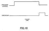
- the boot process of loading a program from an external memory is performed by a program in a processor each time the power is turned on.
- Fig. 10 is a view for describing the timing with which a boot process is performed.
- checksum is performed after a program being loaded from an external memory to judge whether the program was read normally.
- This intermittent receiving is the operation of checking whether the owner of a cellular telephone had a telephone call from a base station.
- a cellular telephone is put into a receiving state in a cycle between, for example, one and two seconds. If there is no incoming call, then the power is disconnected.
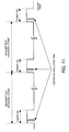
- Fig. 11 is a view for describing an intermittent receiving cycle and checksum time.
- a boot interval is the same as an intermittent receiving cycle in a standby state and is usually 1.28 or 2.56 seconds. If a cellular telephone is in a standby state, power is applied once every intermittent receiving cycle. This intermittent receiving cycle includes program load time and checksum execution time.
- a semiconductor device with an intermittent operation block where application and disconnection of the power are performed periodically and repeatedly.
- This semiconductor device comprises an error check necessity judgment circuit for judging whether an error check must be made on data for booting loaded from an external memory by a boot process performed at the time of power being applied and an error check execution circuit for making an error check on the data for booting in the case of the error check necessity judgment circuit judging that an error check must be made.
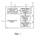
- Fig. 1 is a view showing the theoretical structure of a semiconductor device according to the present invention.
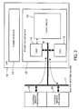
- Fig. 2 is a view showing the structure of the feature of a system necessary for intermittent receiving operation.
- Fig. 3 is a view showing the structure of checksum control.
- Fig. 4 is a flow chart showing the sequence of processes performed regarding boot programs.
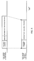
- Fig. 5 is a view showing the difference between time for which the power is in the ON state in the case of checksum being performed and time for which the power is in the ON state in the case of checksum not being performed.
- Fig. 6 is a view showing the details of a checksum control register.
- Fig. 7 is a flow chart showing the sequence of processes performed regarding a boot program which performs checksum forcedly and periodically.
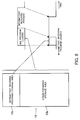
- Fig. 8 is a view showing an example of dividing a program storage area in a memory.
- Fig. 9 is a flow chart showing the sequence of processes performed regarding divided boot programs.
- Fig. 10 is a view for describing the timing with which a boot process is performed.
- Fig. 11 is a view for describing an intermittent receiving cycle and checksum time.
- Fig. 1 is a view showing the theoretical structure of a semiconductor device according to the present invention.
- a semiconductor device 1 comprises a block 2 where power is always applied and an intermittent operation block 3 where application and disconnection of the power are performed periodically and repeatedly.
- the intermittent operation block 3 includes an error check necessity judgment circuit 4 and error check execution circuit 5.
- the block 2 includes an error check necessity notification circuit 6 and error check interval setting circuit 7.
- the error check necessity judgment circuit 4 judges whether an error check must be made on data loaded from an external memory by a boot process performed at the time when power is applied.
- the error check execution circuit 5 makes an error check for confirming whether data was loaded normally in the case of the error check necessity judgment circuit 4 judging that an error check must be made.
- the error check necessity notification circuit 6 located in the block 2 where the power is not disconnected notifies the error check necessity judgment circuit 4 of instructions about whether an error check must be made. Only when the number of times a boot was performed reaches a certain number, the error check interval setting circuit 7 causes the error check necessity notification circuit 6 to notify the error check necessity judgment circuit 4 that an error check must be made.
- the error check necessity notification circuit 6 and error check interval setting circuit 7 are located in the block 2 where the power is not disconnected. Usually the error check necessity notification circuit 6 notifies the error check necessity judgment circuit 4 that an error check is unnecessary.
- the error check interval setting circuit 7 counts the number of times power is applied to the intermittent operation block 3. When the number of times power is applied to the intermittent operation block 3, that is to say, the number of times a boot process is performed as a result of it reaches a certain number, the error check interval setting circuit 7 changes the value set for the error check necessity notification circuit 6 so that an error check will be made.
- the error check interval setting circuit 7 changes the value set for the error check necessity notification circuit 6 so that an error check will be made, and the error check necessity notification circuit 6 notifies the error check necessity judgment circuit 4.
- the error check necessity judgment circuit 4 therefore judges that an error check must be made. In this case, an error check will be made on the data regarding the program for booting after the data is loaded from the external memory.
- the semiconductor device 1 can determine at the time of a boot whether to make an error check on data loaded from an external memory. As a result, there is no need to make an error check every time on data loaded each time a boot is performed. This shortens intermittent operation time by time taken to make these error checks, resulting in a reduction in consumption of power attendant on a useless leakage current.
- the block 2 where power is always applied is within the semiconductor device 1.
- the function of the block 2 may be located outside the semiconductor device 1.
- the semiconductor device 1 includes an input terminal for accepting data indicative of whether an error check must be made, and the error check necessity judgment circuit 4 will judge on data indicative of whether an error check must be made, which is accepted at this input terminal, whether an error check must be made.
- Fig. 2 is a view showing the structure of the feature of a system necessary for intermittent receiving operation.
- the LSI 10 includes a power on block 11 where the power is not turned off and a power on/off block 12 where the power is turned on and off to an intermittent receiving cycle.
- the power on/off block 12 includes a logic circuit 13 including a modem section for modulating and demodulating signals, such as voice, and a CODEC section for performing a scramble process and error correction process, a DSP 14 for controlling the logic circuit 13, a CPU 15 for controlling the entire LSI 10, and an internal bus 16 to which the DSP 14 and LSI 10 are connected.
- the internal bus 16 included in the LSI 10 is connected to an external memory for booting 18 and external memory for saving 19 via an external bus for booting/saving 17.
- the external memory for booting 18 outside the LSI 10 stores a program and the external memory for saving 19 stores data the DSP 14 and CPU 15 handle.
- Fig. 3 is a view showing the structure of checksum control.
- a checksum control register 20 is located in the power on block 11 in the LSI 10 where the power is not turned on or off. This checksum control register 20 holds information indicative of control whether or not checksum is performed as a flag bit. In this case, this flag bit is defined as follows. If the flag bit is "0,” then checksum is performed. If the flag bit is "I,” then checksum is not performed. There is a checksum control port 21 on the DSP 14 and the checksum control register 20 and checksum control port 21 connect by a signal line 22. The checksum control register 20 is controlled via a bus outside the LSI 10 or by an internal CPU. The DSP 14 and checksum control port 21 correspond to the error check necessity judgment circuit 4 shown in Fig. 1, the DSP 14 corresponds to the error check execution circuit 5, and the checksum control register 20 corresponds to the error check necessity notification circuit 6.
- Fig. 4 is a flow chart showing the sequence of processes performed regarding boot programs.
- step S1 when the power to the DSP 14 in the power on/off block 12 is turned on to perform an intermittent receiving process, the DSP 14 loads a program from the external memory for booting 18 into a memory 23 (step S1). After the program being loaded, a port value at the checksum control port 21 connected to the checksum control register 20 is referred to and whether a checksum flag is "0" is judged (step S2). If the checksum flag is "0,” then checksum is performed (step S3) and the boot process is ended. If the checksum flag is "1,” then control is exercised so that the boot process will be ended without checksum being performed.
- Fig. 5 is a view showing the difference between time for which the power is in the ON state in the case of checksum being performed and time for which the power is in the ON state in the case of checksum not being performed.
- checksum is performed at the time when a boot process is performed, then the power is in the ON state for the sum of time taken to load a program, time taken to perform checksum, and time taken to perform an intermittent receiving process of an intermittent receiving cycle.
- time taken to perform checksum can be shortened by time taken to perform checksum. If time for which the power is in the ON state is shortened, consumption of power attendant on a leakage current reduces. As a result, standby time and nonstop telephone call time can be lengthened.
- Fig. 6 is a view showing the details of a checksum control register.
- the checksum control register 20 includes flag bit FLAG and fields CT5 through CT0 for specifying checksum execution interval times. To improve the reliability of a system, control is exercised so that checksum will forcedly be performed one time for the number of times specified in the fields CT5 through CT0 for specifying checksum execution interval times.
- the power to the power on/off block 12 is turned on at the time of intermittent receiving and a boot process is performed. It is assumed that checksum execution interval times is set to, for example, 20. Then when the number of times this boot process is performed reaches 20, control is exercised so that checksum will forcedly be performed.
- the fields CT5 through CT0 in the checksum control register 20 correspond to the error check interval setting circuit 7 shown in Fig. 1.
- Fig. 7 is a flow chart showing the sequence of processes performed regarding a boot program which performs checksum forcedly and periodically.
- the DSP 14 loads a program from the external memory for booting 18 into the memory 23 (step S11). After the program being loaded, a port value at the checksum control port 21 connected to the checksum control register 20 is referred to and whether a checksum flag is "0" is judged (step S12). If the checksum flag is "0,” then checksum is performed (step S13) and the boot process is ended. If the checksum flag is "1,” then whether the number of times a boot process was performed has reached a checksum execution interval times is judged (stap S14).
- step S13 If the number of times a boot process was performed has reached the checksum execution interval times, then checksum is performed forcedly (step S13) and the boot process is ended. If the number of times a boot process was performed has not reached the checksum execution interval times, then the boot process is ended without checksum being performed.
- time needed for program load performed at the time when a boot process is performed can be shortened further. Now, a method for shortening time needed for program load will be described.
- Fig. 8 is a view showing an example of dividing a program storage area in a memory.
- the external memory for booting 18 which stores programs is divided into an intermittent receiving programs storage area 18a and other programs storage area 18b.
- the intermittent receiving programs storage area 18a stores only programs needed for an intermittent receiving process and the other programs storage area 18b stores other programs, such as one for a telephone call process.
- Programs stored in the other programs storage area 18b will additionally be loaded if there is an incoming call as a result of the intermittent receiving process.
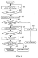
- Fig. 9 is a flow chart showing the sequence of processes performed regarding divided boot programs.
- step S21 when the power to the DSP 14 in the power on/off block 12 is turned on to perform an intermittent receiving process, the DSP 14 loads a program for intermittent receiving from the intermittent receiving programs storage area 18a in the external memory for booting 18 into the memory 23 (step S21). After the program for intermittent receiving being loaded, checksum is performed to judge whether an error occurred (step S22). If an error occurred, then step S21 is repeated to reload the program for intermittent receiving. If an error is not detected by the checksum (or if checksum is omitted) , then an intermittent receiving process is performed (step S23). By performing the intermittent receiving process, whether there is a local group incoming call is judged (step S24).
- step S25 If there is a local group incoming call, the DSP 14 loads other programs from the other programs storage area 18b in the external memory for booting 18 (step S25). After the other programs being loaded, checksum is performed to judge whether an error occurred (step S26). If an error occurred, then step S25 is repeated to reload the other programs. If an error is not detected by the checksum (or if checksum is omitted), then local group incoming call processing is performed (step S27). Whether the result of the decoding of a message is normal is judged by this local group incoming call processing (step S28). If the result of the decoding of the message is normal, then incoming call processing is performed (S29). If the result of the decoding of the message is abnormal, then error processing is performed (step S30).
- step S24 If the judgment that there is no local group incoming call is made in step S24, then data the DSP 14 and CPU 15 were processing is saved in the external memory for saving 19 (step S31) and the power is turned off.
- the semiconductor device includes an error check necessity judgment circuit for judging whether an error check must be made on data for booting loaded from an external memory at the time of a boot, and an error check will be made in accordance with a judgment made by the error check necessity judgment circuit.
- an error check which is made on data for booting each time intermittent operation is performed can be omitted. Therefore, time taken to perform error check processes can be shortened. That is to say, time for which the power is in the ON state can be shortened and consumption of power attendant on a leakage current can be reduced.
- a reduction in consumption of power attendant on a leakage current will lengthen the lives of batteries. Moreover, smaller capacity batteries with the same life can be used, resulting in more compact, lighter portable remote terminal units.
Landscapes
- Engineering & Computer Science (AREA)
- Computer Networks & Wireless Communication (AREA)
- Signal Processing (AREA)
- Mobile Radio Communication Systems (AREA)
- Telephone Function (AREA)
- Power Sources (AREA)
- Techniques For Improving Reliability Of Storages (AREA)
Abstract
Description
Claims (14)
- A semiconductor device with an intermittent operation block where application and disconnection of power are performed periodically and repeatedly, the semiconductor device comprising:an error check necessity judgment circuit for judging whether an error check must be made on data for booting loaded from an external memory by a boot process performed at the time of power being applied; andan error check execution circuit for making an error check on the data for booting in the case of the error check necessity judgment circuit judging that an error check must be made.
- The semiconductor device according to claim 1, further comprising an input terminal for accepting error check necessity data to give instructions from the outside about whether an error check must be made, wherein the error check necessity judgment circuit judges on the error check necessity data of which the error check necessity judgment circuit is notified from the outside whether an error check must be made.
- The semiconductor device according to claim 1 or 2, further comprising an error check necessity notification circuit for notifying the error check necessity judgment circuit of error check necessity data to give instructions about whether an error check must be made.
- The semiconductor device according to claim 3, wherein the error check necessity notification circuit is located in a block where power is not disconnected.
- The semiconductor device according to claim 3 or 4, wherein the error check necessity notification circuit is a control register which stores a flag bit indicative of whether an error check must be made.
- The semiconductor device according to claim 3, 4 or 5, further comprising an error check interval setting circuit for forcedly setting error check necessity data of which the error check necessity notification circuit notifies the error check necessity judgment circuit to data indicative that an error check must be made only at the time of the number of times a boot is performed reaching a certain number.
- The semiconductor device according to claim 6, wherein the error check interval setting circuit is located in a block where power is not disconnected.
- The semiconductor device according to claim 6 or 7, wherein the error check interval setting circuit can arbitrarily set the number of times the boot is performed, being a cycle in which an error check is made.
- A portable remote terminal unit in which power to blocks unnecessary for an intermittent receiving control process is disconnected for a period when the unit in a standby state does not perform intermittent receiving, the portable remote terminal unit comprising:an error check necessity judgment circuit for judging whether an error check must be made on data for booting loaded from a memory where power is not disconnected by a boot process performed at the time of power being applied to perform the intermittent receiving;an error check execution circuit for making an error check on the data for booting in the case of the error check necessity judgment circuit judging that an error check must be made;an error check necessity notification circuit for notifying the error check necessity judgment circuit whether an error check must be made; andan error check interval setting circuit for causing the error check necessity notification circuit to notify the error check necessity judgment circuit that an error check must be made at the time of the number of times a boot is performed reaching a certain number.
- The portable remote terminal unit according to claim 9, wherein the error check necessity notification circuit and the error check interval setting circuit are located in a block where power is not disconnected.
- The portable remote terminal unit according to claim 9 or 10, wherein the error check interval setting circuit can arbitrarily set the number of times the boot is performed, being a cycle in which an error check is made.
- An intermittent receiving method in which power to blocks in a portable remote terminal unit unnecessary for an intermittent receiving control process is disconnected for a period when the unit in a standby state does not perform intermittent receiving, the intermittent receiving method comprising the steps of:applying power to blocks in the portable remote terminal unit necessary for an intermittent receiving control process at the time of intermittent receiving;loading only a program necessary for the intermittent receiving control process from an external memory;judging whether the number of times a boot is performed has reached a certain number; andmaking an error check on the program loaded at the time of the number of times the boot is performed reaching a certain number.
- The intermittent receiving method according to claim 12, further comprising the step of loading remaining programs from the memory in the case of there being a local group incoming call at the time of the intermittent receiving control process.
- A portable remote terminal unit in which power to blocks unnecessary for an intermittent receiving control process is disconnected for a period when the unit in a standby state does not perform intermittent receiving, the portable remote terminal unit comprising:an error check necessity judgment circuit for judging whether an error check must be made on data for booting loaded from a memory where power is not disconnected by a boot process performed at the time of power being applied to perform the intermittent receiving; andan error check execution circuit for making an error check on the data for booting in the case of the error check necessity judgment circuit judging that an error check must be made.
Applications Claiming Priority (2)
| Application Number | Priority Date | Filing Date | Title |
|---|---|---|---|
| JP2001384256 | 2001-12-18 | ||
| JP2001384256A JP4162401B2 (en) | 2001-12-18 | 2001-12-18 | Portable terminal device and intermittent reception method |
Publications (3)
| Publication Number | Publication Date |
|---|---|
| EP1322100A2 true EP1322100A2 (en) | 2003-06-25 |
| EP1322100A3 EP1322100A3 (en) | 2004-05-06 |
| EP1322100B1 EP1322100B1 (en) | 2006-10-18 |
Family
ID=19187707
Family Applications (1)
| Application Number | Title | Priority Date | Filing Date |
|---|---|---|---|
| EP02255670A Expired - Lifetime EP1322100B1 (en) | 2001-12-18 | 2002-08-14 | Semiconductor device, portable remote terminal unit and intermittent receiving method |
Country Status (7)
| Country | Link |
|---|---|
| US (1) | US7007202B2 (en) |
| EP (1) | EP1322100B1 (en) |
| JP (1) | JP4162401B2 (en) |
| KR (1) | KR100838008B1 (en) |
| CN (1) | CN1194379C (en) |
| DE (1) | DE60215445T2 (en) |
| TW (1) | TW556419B (en) |
Cited By (1)
| Publication number | Priority date | Publication date | Assignee | Title |
|---|---|---|---|---|
| US8135991B2 (en) | 2004-01-28 | 2012-03-13 | Sony Corporation | Semiconductor device and processing method for starting the same |
Families Citing this family (10)
| Publication number | Priority date | Publication date | Assignee | Title |
|---|---|---|---|---|
| JP2003209616A (en) * | 2002-01-15 | 2003-07-25 | Fujitsu Ltd | Semiconductor device and portable terminal device |
| US20050066206A1 (en) * | 2003-09-24 | 2005-03-24 | John Beers | Storage device configuration |
| JP4601968B2 (en) * | 2004-01-19 | 2010-12-22 | 大日本印刷株式会社 | IC card and IC card program that eliminates data integrity check |
| US7266727B2 (en) * | 2004-03-18 | 2007-09-04 | International Business Machines Corporation | Computer boot operation utilizing targeted boot diagnostics |
| US7590918B2 (en) * | 2004-09-10 | 2009-09-15 | Ovonyx, Inc. | Using a phase change memory as a high volume memory |
| JP4556581B2 (en) * | 2004-09-14 | 2010-10-06 | 日本電気株式会社 | Portable terminal device, portable terminal control method, and program |
| CN101375530B (en) * | 2006-02-08 | 2014-03-19 | 日本电气株式会社 | Portable mobile terminal and communicating method |
| JP2009177774A (en) * | 2007-12-27 | 2009-08-06 | Kyocera Corp | Signal processing apparatus, portable communication terminal apparatus, and wireless communication system |
| US8495601B2 (en) | 2010-06-09 | 2013-07-23 | Lear Corporation | Shared memory architecture |
| US8539472B2 (en) | 2010-06-09 | 2013-09-17 | Lear Corporation | Method and system of updating shared memory |
Family Cites Families (9)
| Publication number | Priority date | Publication date | Assignee | Title |
|---|---|---|---|---|
| US5390324A (en) * | 1992-10-02 | 1995-02-14 | Compaq Computer Corporation | Computer failure recovery and alert system |
| EP0613094A3 (en) * | 1993-02-25 | 1994-11-09 | Fluke Corp | Signal processing system with digital signal processor based CPU. |
| US6381694B1 (en) * | 1994-02-18 | 2002-04-30 | Apple Computer, Inc. | System for automatic recovery from software problems that cause computer failure |
| US5910944A (en) * | 1997-02-28 | 1999-06-08 | Motorola, Inc. | Radio telephone and method for operating a radiotelephone in slotted paging mode |
| US5978913A (en) * | 1998-03-05 | 1999-11-02 | Compaq Computer Corporation | Computer with periodic full power-on self test |
| US6807643B2 (en) * | 1998-12-29 | 2004-10-19 | Intel Corporation | Method and apparatus for providing diagnosis of a processor without an operating system boot |
| US6640316B1 (en) * | 2000-05-23 | 2003-10-28 | Dell Products L.P. | Boot recovery of simple boot BIOS |
| JP4434539B2 (en) * | 2001-12-26 | 2010-03-17 | 富士通マイクロエレクトロニクス株式会社 | Processor and boot method thereof |
| US7010723B2 (en) * | 2002-02-11 | 2006-03-07 | Intel Corporation | Method to couple integrated circuit packages to bonding pads having vias |
-
2001
- 2001-12-18 JP JP2001384256A patent/JP4162401B2/en not_active Expired - Fee Related
-
2002
- 2002-08-14 EP EP02255670A patent/EP1322100B1/en not_active Expired - Lifetime
- 2002-08-14 DE DE60215445T patent/DE60215445T2/en not_active Expired - Lifetime
- 2002-08-15 TW TW091118454A patent/TW556419B/en not_active IP Right Cessation
- 2002-08-20 US US10/223,468 patent/US7007202B2/en not_active Expired - Lifetime
- 2002-09-06 CN CNB021318409A patent/CN1194379C/en not_active Expired - Fee Related
- 2002-09-07 KR KR1020020054006A patent/KR100838008B1/en not_active Expired - Fee Related
Cited By (1)
| Publication number | Priority date | Publication date | Assignee | Title |
|---|---|---|---|---|
| US8135991B2 (en) | 2004-01-28 | 2012-03-13 | Sony Corporation | Semiconductor device and processing method for starting the same |
Also Published As
| Publication number | Publication date |
|---|---|
| KR20030051179A (en) | 2003-06-25 |
| US7007202B2 (en) | 2006-02-28 |
| KR100838008B1 (en) | 2008-06-12 |
| CN1194379C (en) | 2005-03-23 |
| US20030115507A1 (en) | 2003-06-19 |
| CN1427448A (en) | 2003-07-02 |
| JP2003188798A (en) | 2003-07-04 |
| EP1322100B1 (en) | 2006-10-18 |
| DE60215445T2 (en) | 2007-02-01 |
| TW556419B (en) | 2003-10-01 |
| JP4162401B2 (en) | 2008-10-08 |
| EP1322100A3 (en) | 2004-05-06 |
| DE60215445D1 (en) | 2006-11-30 |
Similar Documents
| Publication | Publication Date | Title |
|---|---|---|
| EP1322100B1 (en) | Semiconductor device, portable remote terminal unit and intermittent receiving method | |
| US20040082362A1 (en) | Method for power management of a smart phone | |
| CN102792647A (en) | Explicit congestion notification based rate adaptation using binary marking in communication systems | |
| US20100081485A1 (en) | Apparatus, system and method capable of integrating a cellular phone stack in an extended firmware interface (efi) layer | |
| CN1283375A (en) | Method of increasing bettery life in mobile communications devices which use paging channel displaement | |
| US8130698B2 (en) | Changing an operation state and recovering a network of a WLAN device | |
| US7764969B2 (en) | Reduced paging cycles in a wireless communication system | |
| JP2007536667A (en) | Mobile device with integrated circuit and method for powering down such a circuit | |
| US8526398B2 (en) | Communication terminal and communication method | |
| KR101026831B1 (en) | Semiconductor device and electronic device | |
| US20090016313A1 (en) | Method and apparatus for switching a communication channel | |
| JP4693870B2 (en) | Semiconductor device | |
| CN112533268B (en) | Terminal and processing method thereof | |
| KR20050085395A (en) | System and method for software download to wireless communication device | |
| JPH1078835A (en) | Portable terminal equipment | |
| JP2002291172A (en) | Power supply method and communication device | |
| US7724894B2 (en) | Maintaining line voltage during reset | |
| JP2991165B2 (en) | Terminal equipment for ISDN | |
| JPH04355524A (en) | Portable radio terminal equipment | |
| KR100369634B1 (en) | Apparatus and Method for GPS clock monitoring and operational controlling in a mobile communication BTS | |
| KR100382474B1 (en) | Selector/Vocoder in mobile communication system and data processing metod using the same | |
| CN112165389A (en) | A system and method for server data protection based on power over Ethernet | |
| KR20230073674A (en) | apparatus and method for detecting cause of re-booting for hardware equipment | |
| JP5391260B2 (en) | Information processing apparatus and data output method | |
| CN111039120A (en) | Elevator state alarm method and device |
Legal Events
| Date | Code | Title | Description |
|---|---|---|---|
| PUAI | Public reference made under article 153(3) epc to a published international application that has entered the european phase |
Free format text: ORIGINAL CODE: 0009012 |
|
| AK | Designated contracting states |
Designated state(s): AT BE BG CH CY CZ DE DK EE ES FI FR GB GR IE IT LI LU MC NL PT SE SK TR |
|
| AX | Request for extension of the european patent |
Extension state: AL LT LV MK RO SI |
|
| PUAL | Search report despatched |
Free format text: ORIGINAL CODE: 0009013 |
|
| AK | Designated contracting states |
Kind code of ref document: A3 Designated state(s): AT BE BG CH CY CZ DE DK EE ES FI FR GB GR IE IT LI LU MC NL PT SE SK TR |
|
| AX | Request for extension of the european patent |
Extension state: AL LT LV MK RO SI |
|
| RIC1 | Information provided on ipc code assigned before grant |
Ipc: 7H 04M 1/73 A Ipc: 7H 04B 1/16 B Ipc: 7G 06F 9/445 B Ipc: 7H 04Q 7/32 B |
|
| 17P | Request for examination filed |
Effective date: 20040609 |
|
| 17Q | First examination report despatched |
Effective date: 20040806 |
|
| AKX | Designation fees paid |
Designated state(s): DE FR GB |
|
| GRAP | Despatch of communication of intention to grant a patent |
Free format text: ORIGINAL CODE: EPIDOSNIGR1 |
|
| GRAS | Grant fee paid |
Free format text: ORIGINAL CODE: EPIDOSNIGR3 |
|
| GRAA | (expected) grant |
Free format text: ORIGINAL CODE: 0009210 |
|
| AK | Designated contracting states |
Kind code of ref document: B1 Designated state(s): DE FR GB |
|
| REG | Reference to a national code |
Ref country code: GB Ref legal event code: FG4D |
|
| REF | Corresponds to: |
Ref document number: 60215445 Country of ref document: DE Date of ref document: 20061130 Kind code of ref document: P |
|
| ET | Fr: translation filed | ||
| PLBE | No opposition filed within time limit |
Free format text: ORIGINAL CODE: 0009261 |
|
| STAA | Information on the status of an ep patent application or granted ep patent |
Free format text: STATUS: NO OPPOSITION FILED WITHIN TIME LIMIT |
|
| 26N | No opposition filed |
Effective date: 20070719 |
|
| REG | Reference to a national code |
Ref country code: GB Ref legal event code: 732E |
|
| REG | Reference to a national code |
Ref country code: FR Ref legal event code: TP |
|
| PGFP | Annual fee paid to national office [announced via postgrant information from national office to epo] |
Ref country code: FR Payment date: 20090814 Year of fee payment: 8 |
|
| PGFP | Annual fee paid to national office [announced via postgrant information from national office to epo] |
Ref country code: GB Payment date: 20090812 Year of fee payment: 8 |
|
| GBPC | Gb: european patent ceased through non-payment of renewal fee |
Effective date: 20100814 |
|
| REG | Reference to a national code |
Ref country code: FR Ref legal event code: ST Effective date: 20110502 |
|
| PG25 | Lapsed in a contracting state [announced via postgrant information from national office to epo] |
Ref country code: FR Free format text: LAPSE BECAUSE OF NON-PAYMENT OF DUE FEES Effective date: 20100831 |
|
| PG25 | Lapsed in a contracting state [announced via postgrant information from national office to epo] |
Ref country code: GB Free format text: LAPSE BECAUSE OF NON-PAYMENT OF DUE FEES Effective date: 20100814 |
|
| REG | Reference to a national code |
Ref country code: DE Ref legal event code: R082 Ref document number: 60215445 Country of ref document: DE Representative=s name: REICHERT & LINDNER PARTNERSCHAFT PATENTANWAELT, DE |
|
| REG | Reference to a national code |
Ref country code: DE Ref legal event code: R081 Ref document number: 60215445 Country of ref document: DE Owner name: SOCIONEXT INC., YOKOHAMA-SHI, JP Free format text: FORMER OWNER: FUJITSU SEMICONDUCTOR LTD., YOKOHAMA, KANAGAWA, JP Effective date: 20150512 Ref country code: DE Ref legal event code: R082 Ref document number: 60215445 Country of ref document: DE Representative=s name: REICHERT & LINDNER PARTNERSCHAFT PATENTANWAELT, DE Effective date: 20150512 |
|
| PGFP | Annual fee paid to national office [announced via postgrant information from national office to epo] |
Ref country code: DE Payment date: 20180731 Year of fee payment: 17 |
|
| REG | Reference to a national code |
Ref country code: DE Ref legal event code: R119 Ref document number: 60215445 Country of ref document: DE |
|
| PG25 | Lapsed in a contracting state [announced via postgrant information from national office to epo] |
Ref country code: DE Free format text: LAPSE BECAUSE OF NON-PAYMENT OF DUE FEES Effective date: 20200303 |