EP1321977A1 - Method for reducing residual electric charge created by a previous process step on a conductive structure - Google Patents
Method for reducing residual electric charge created by a previous process step on a conductive structure Download PDFInfo
- Publication number
- EP1321977A1 EP1321977A1 EP01403276A EP01403276A EP1321977A1 EP 1321977 A1 EP1321977 A1 EP 1321977A1 EP 01403276 A EP01403276 A EP 01403276A EP 01403276 A EP01403276 A EP 01403276A EP 1321977 A1 EP1321977 A1 EP 1321977A1
- Authority
- EP
- European Patent Office
- Prior art keywords
- plasma
- plasma treatment
- treatment
- gas
- conductive structure
- Prior art date
- Legal status (The legal status is an assumption and is not a legal conclusion. Google has not performed a legal analysis and makes no representation as to the accuracy of the status listed.)
- Ceased
Links
Images


Classifications
-
- H—ELECTRICITY
- H10—SEMICONDUCTOR DEVICES; ELECTRIC SOLID-STATE DEVICES NOT OTHERWISE PROVIDED FOR
- H10P—GENERIC PROCESSES OR APPARATUS FOR THE MANUFACTURE OR TREATMENT OF DEVICES COVERED BY CLASS H10
- H10P70/00—Cleaning of wafers, substrates or parts of devices
- H10P70/20—Cleaning during device manufacture
- H10P70/27—Cleaning during device manufacture during, before or after processing of conductive materials, e.g. polysilicon or amorphous silicon layers
- H10P70/273—Cleaning during device manufacture during, before or after processing of conductive materials, e.g. polysilicon or amorphous silicon layers the processing being a delineation of conductive layers, e.g. by RIE
-
- H—ELECTRICITY
- H10—SEMICONDUCTOR DEVICES; ELECTRIC SOLID-STATE DEVICES NOT OTHERWISE PROVIDED FOR
- H10P—GENERIC PROCESSES OR APPARATUS FOR THE MANUFACTURE OR TREATMENT OF DEVICES COVERED BY CLASS H10
- H10P50/00—Etching of wafers, substrates or parts of devices
- H10P50/20—Dry etching; Plasma etching; Reactive-ion etching
- H10P50/26—Dry etching; Plasma etching; Reactive-ion etching of conductive or resistive materials
- H10P50/264—Dry etching; Plasma etching; Reactive-ion etching of conductive or resistive materials by chemical means
- H10P50/266—Dry etching; Plasma etching; Reactive-ion etching of conductive or resistive materials by chemical means by vapour etching only
- H10P50/267—Dry etching; Plasma etching; Reactive-ion etching of conductive or resistive materials by chemical means by vapour etching only using plasmas
-
- H—ELECTRICITY
- H10—SEMICONDUCTOR DEVICES; ELECTRIC SOLID-STATE DEVICES NOT OTHERWISE PROVIDED FOR
- H10P—GENERIC PROCESSES OR APPARATUS FOR THE MANUFACTURE OR TREATMENT OF DEVICES COVERED BY CLASS H10
- H10P50/00—Etching of wafers, substrates or parts of devices
- H10P50/20—Dry etching; Plasma etching; Reactive-ion etching
- H10P50/28—Dry etching; Plasma etching; Reactive-ion etching of insulating materials
- H10P50/286—Dry etching; Plasma etching; Reactive-ion etching of insulating materials of organic materials
- H10P50/287—Dry etching; Plasma etching; Reactive-ion etching of insulating materials of organic materials by chemical means
Definitions
- the invention relates to a method for reducing a residual electric charge created by a previous process step, particularly a plasma treatment, on a conductive structure, particularly in a semiconductor integrated circuit.
- the manufacturing of a semiconductor integrated circuit comprises plasma treatments, for instance the plasma etching of conductive layers such as interconnects, or the plasma removal of an organic mask used for patterning a conductive layer.
- the wafer is subjected to an additional step to remove or neutralise the residual charges on the conductive structures.
- US patent No. 6.093.658 discloses a method for manufacturing a semiconductor IC, wherein the wafer is exposed to an electron dose of 5.000 ⁇ C/cm 2 to 25.000 ⁇ C/cm 2 which is configured to neutralise the electric charge that is built up in a metallisation layer patterned by plasma etching. This method, however, requires an electron beam system which is no typical system to use in the manufacturing of semiconductor IC's and which is relatively expensive.
- the invention seeks to provide a simple and economic method for reducing a residual electric charge created by a previous process step on a conductive structure.
- this object is accomplished by submitting the wafer with the conductive structures to a plasma treatment having a discharging effect.
- the plasma treatment may be performed as a stand alone step with selected gas composition of the plasma and/or other parameters like applied power and process pressure
- the discharging treatment may be done at the end of this former plasma treatment by altering the gas composition of the plasma and/or other parameters of the plasma treatment, such as the applied power or process pressure.
- a suitable gas composition for the discharging plasma treatment may contain Hydrogen, Helium, Argon or Fluorine or a mixture of two or more of these gases.
- Hydrogen containing gas may be Forming-gas or water vapour.
- the recommended source of Fluorine in the plasma is CF 4 , NF 3 , SF 6 , CHF 3 , or C 2 F 6 gas.
- the discharging plasma treatment may, at least partly, constitute a step of the complete process, for example the removal of an organic mask by a plasma treatment.
- the subject invention has as purpose to neutralize charges that are built up during previous plasma treatment of layers during the manufacturing of an integrated circuit.
- a first example will be described with reference to figure 1, wherein the plasma treatment deals with the top metal layer 5.
- Figure 1 further shows a patterned conductive layer 3 created on an insulating layer 2, for instance of silicon dioxide.
- This conductive layer 3 is a layer of metal interconnects or interconnects of amorphous or polycrystalline silicon.
- the insulating layer 2 is for example created on a substrate 1 of silicon whereon Integrated Circuit devices (not shown) are created.
- the conductive layer 3, e.g. a Al/Cu metallisation layer, is formed over the layer 2.
- a following insulating dielectric layer 4 is deposited on the conductive layer 3 and the dielectric layer 2.
- This following dielectric layer 4 may be planarised using for instance a conventional Chemical Mechanical Polishing technique.
- a second interconnect layer is created above the dielectric layer 4, but to interconnect both layers 3 and 5, holes 6 are formed in the dielectric layer 4 and filled with tungsten to form tungsten plugs 7 before the metallisation layer 5 is deposited.
- the via holes 6 are made by standard photolitography and etching.
- the patterned metallisation layer 5 is formed as shown in the block diagram of figure 2.
- a continuous metallisation layer for instance from W, Al/Cu or Al/Si/Cu is deposited, for instance sputtered, on the complete wafer surface
- the continuous metallisation layer is then patterned using conventional photolithography and plasma etching techniques.
- a photoresist organic mask is formed on top of the metallisation layer by forming a photoresist layer on this metallisation layer, selectively exposing the photoresist to light of short wavelenght through a patterned reticle and developing the photoresist.
- the obtained wafer is introduced in a plasma etcher wherein successively are performed a plasma etching operation 11 on the metal wherein the exposed parts of the metallisation layer are etched away, and a stripping operation 12 wherein the mask is removed in situ.
- a plasma etching operation 11 on the metal wherein the exposed parts of the metallisation layer are etched away
- a stripping operation 12 wherein the mask is removed in situ.
- the patterned metallisation layer 5 as well as the first mentioned conductive layer 3 are not always electrically connected to the substrate 1. Consequently, these layers and the tungsten plugs will be electrically charged by the plasma etching operations 11 and 12.
- the wafer is transferred to an ex-situ plasma module wherein the wafer is subjected to an operation 13, i.e. a treatment with a plasma containing Fluorine, Hydrogen, Argon, Helium or a mixture of two or more of these gases.
- an operation 13 i.e. a treatment with a plasma containing Fluorine, Hydrogen, Argon, Helium or a mixture of two or more of these gases.
- Forming-gas a mixture of H 2 and N 2
- water vapour H 2 O
- Oxygen or Oxygen containing gas may be added to the plasma.
- Oxygen and Oxygen containing additives may facilitate the removal of the organic mask.
- a cleaning operation 14 is accomplished which consists of immersing the obtained wafer in a solvent to remove any polymer residues produced during the plasma etching.
- an Al/Cu metallisation layer is sputtered (operation 8), and an i-line photoresist mask is formed using conventional photolithography (operation 9).
- This metallisation layer is plasma etched (operation 11) and the photoresist mask is plasma stripped in-situ using cluster P-5000 tool including a MxP etch chamber and a downstream strip chamber of Applied Materials (operation 12).
- the substrate is treated in a GaSonics L3300 plasma etch system (operation 13).
- the parameters of the plasma treatment 13 are as follows: Pressure 700 m Torr (0,0933 kPa) RF Power 600 W Forming-gas flow rate 950 sccm (standard cm 3 ) N 2 O flow rate 10 sccm Platen temperature 250°C Process time 20 sec
- the metallisation layer 5 has received an electric charge, for instance during the plasma steps (operations 11 and 12), the last mentioned plasma treatment (operation 13) removes this charge.
- the substrate is moved to a Semitool spray cleaning station for removal of residual polymers in EKC265 solvent (operation 14).
- Example 1 is repeated but the plasma treatment (operation 13) is performed in a Lam 4520XL plasma etch system and with the following parameters: Pressure 450 m Torr (0,0600 kPa) RF Power top 200 W RF Power bottom 200 W CF 4 flow rate 10 sccm O 2 flow rate 400 sccm Electrode temperature 40°C/20°C (Top/Bottom) He pressure 15 Torr (2,0000 kPa) Process time 20 sec
- Example 2 is repeated but the plasma treatment in a Lam 4520XL plasma etch system (operation 13) is performed with the following parameters: Pressure 200 m Torr (0,02667 kPa) RF Power top 200 W RF Power bottom 200 W Ar flow rate 250 sccm Electrode temperature 40°C/20°C (Top/Bottom) He pressure 15 Torr (2,0000 kPa) Process time 20 sec
- Example 3 is repeated but the plasma treatment (operation 13) is performed in an isotropic etch module of Lam 4500i plasma etch system and with the following parameters: Pressure 1000 m Torr (0,1333 kPa) RF Power 600 W He flow rate 200 sccm Paddle temperature 100°C Process time 20 sec
- the patterned metallisation layer 5 is obtained as shown in the diagram of figure 3.
- the method differs from the above embodiment as shown in figure 2 in that the treatment with plasma containing F, H or a mixture of F and H (operation 13) is not performed ex-situ, but in-situ, this is in the same equipment used for etching the metal and for stripping the resist.
- an Al/Cu metallisation layer is sputtered (operation 8), and an i-line photoresist mask is formed using conventional photolithography (operation 9).
- This metallisation layer is plasma etched (operation 11) using a MxP etch chamber mounted on a P-5000 cluster tool of Applied Materials.
- the photoresist mask is then stripped in a plasma using a downstream strip chamber mounted on the same P-5000 cluster unit. This stripping process is performed in three phases each with different parameters.
- the first phase is used for removing the Chlorine-containing residues of the mask to prevent further corrosion of the Al/Cu layer 5.
- the second phase is the main resist strip step.
- the third phase which is relatively short compared to said previous phases, has the function of the plasma treatment 13 of the embodiment of figure 2, this is mainly to remove or reduce the electric charge built up during the second phase.
- the substrate is moved to a Semitool spray cleaning station for removal of residual polymers in EKC265 solvent (operation 14).
- Figure 4 shows another example of an integrated circuit which is manufactured as follows (with reference to figures 3 and 4):
- Integrated Circuit(IC) MOS transistor devices are created on a Silicon substrate 1. This includes at least a formation of field oxide insulation areas 15 and free of field oxide active areas 16, a formation of thin gate oxide 17 on top of field oxide active areas 16, a deposition and patterning of polysilicon-gates 18 of the MOS transistors and a formation of source/drain areas of the transistors.
- a silicon oxide dielectric layer 2 is deposited over the devices that are formed on the substrate 1, and via holes 6 are formed through the dielectric layer 2 to the gates 18 and active areas 16 below.
- a tungsten interconnect layer 19 is deposited then (operation 8), and an i-line photoresist mask is formed using conventional photolithography (operation 9).
- the tungsten layer 19 is plasma etched using MxP etch chamber mounted on a P-5000 cluster tool of Applied Materials (operation 11), and the photoresist mask is stripped in plasma using a downstream strip chamber mounted on the same P-5000 cluster unit.
- the parameters of the resist strip process (operation 12) are : Phase 1 Phase 2 Pressure, Torr (kPa) 2(0,2666) 2(0,2666) RF Power, W 1000 1000 O 2 flow rate, sccm 3000 N 2 flow rate, sccm 200 H 2 O flow rate, sccm 500 Temperature, °C 250 250 Process time, sec 90 10
- phase 2 The last phase of the resist strip process (phase 2) is designed to remove the electrical charge built up on the conductive structures of polysilicon gates 18 and the tungsten interconnects 19 connected to them, during the main resist removal step and/or during the plasma etch of these tungsten interconnects. If the charge is not removed until the next operation, it keeps an electrical stress on the gate oxide dielectric and increases the chance of a breaking it down. That, in turn, reduces the reliability of the IC.
Landscapes
- Drying Of Semiconductors (AREA)
- Internal Circuitry In Semiconductor Integrated Circuit Devices (AREA)
Abstract
Description
- The invention relates to a method for reducing a residual electric charge created by a previous process step, particularly a plasma treatment, on a conductive structure, particularly in a semiconductor integrated circuit.
- The manufacturing of a semiconductor integrated circuit comprises plasma treatments, for instance the plasma etching of conductive layers such as interconnects, or the plasma removal of an organic mask used for patterning a conductive layer.
- As is well known, such plasma treatments might cause conductive layers to be electrically charged. Charges of the conductive layers should be avoided as they can negatively influence the lifetime of the integrated circuit.
- Therefore, after plasma treatment, the wafer is subjected to an additional step to remove or neutralise the residual charges on the conductive structures.
- According to US patent No. 6.077.762 the electric charge of the metallisation layer built-up during plasma etching is neutralised by contacting this layer with a conductive liquid, particularly a liquid metal such as mercury, which is electrically grounded. However, the use of a liquid conductive metal is rather unconventional in semiconductor processing, and is complicated and expensive.
- US patent No. 6.093.658 discloses a method for manufacturing a semiconductor IC, wherein the wafer is exposed to an electron dose of 5.000 µC/cm2 to 25.000 µC/cm2 which is configured to neutralise the electric charge that is built up in a metallisation layer patterned by plasma etching. This method, however, requires an electron beam system which is no typical system to use in the manufacturing of semiconductor IC's and which is relatively expensive.
- The invention seeks to provide a simple and economic method for reducing a residual electric charge created by a previous process step on a conductive structure.
- In accordance with the invention, this object is accomplished by submitting the wafer with the conductive structures to a plasma treatment having a discharging effect.
- The plasma treatment may be performed as a stand alone step with selected gas composition of the plasma and/or other parameters like applied power and process pressure
- If the charge has been created by a plasma treatment, the discharging treatment may be done at the end of this former plasma treatment by altering the gas composition of the plasma and/or other parameters of the plasma treatment, such as the applied power or process pressure.
- A suitable gas composition for the discharging plasma treatment may contain Hydrogen, Helium, Argon or Fluorine or a mixture of two or more of these gases. Hydrogen containing gas may be Forming-gas or water vapour. When the plasma contains fluorine, the recommended source of Fluorine in the plasma is CF4, NF3, SF6, CHF3, or C2F6 gas.
- In some cases, the discharging plasma treatment may, at least partly, constitute a step of the complete process, for example the removal of an organic mask by a plasma treatment.
- Details and characteristics of the invention will appear from the following description in which reference is made to the attached drawings wherein:
- Figure 1 shows schematically a portion of a section of an integrated circuit;
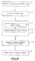
- Figure 2 is a block diagram of the last steps of the method for manufacturing the semiconductor device of figure 1, comprising the reduction of residual electric charges according to the invention;
- Figure 3 is a block diagram similar to the one of Figure 2, but pertaining to another form of embodiment of the invention;
- Figure 4 shows a portion of a section of an integrated circuit similar to the one of figure 1, but pertaining to another form of embodiment, manufactured with application of the method of the invention.
-
- The subject invention has as purpose to neutralize charges that are built up during previous plasma treatment of layers during the manufacturing of an integrated circuit. A first example will be described with reference to figure 1, wherein the plasma treatment deals with the top metal layer 5.
- Figure 1 further shows a patterned conductive layer 3 created on an
insulating layer 2, for instance of silicon dioxide. - This conductive layer 3 is a layer of metal interconnects or interconnects of amorphous or polycrystalline silicon.
- The
insulating layer 2 is for example created on asubstrate 1 of silicon whereon Integrated Circuit devices (not shown) are created. The conductive layer 3, e.g. a Al/Cu metallisation layer, is formed over thelayer 2. - A following insulating dielectric layer 4 is deposited on the conductive layer 3 and the
dielectric layer 2. This following dielectric layer 4 may be planarised using for instance a conventional Chemical Mechanical Polishing technique. - A second interconnect layer, this is the metallisation layer 5, is created above the dielectric layer 4, but to interconnect both layers 3 and 5, holes 6 are formed in the dielectric layer 4 and filled with tungsten to form
tungsten plugs 7 before the metallisation layer 5 is deposited. - The via holes 6 are made by standard photolitography and etching.
- The patterned metallisation layer 5 is formed as shown in the block diagram of figure 2.
- In a
first operation 8, a continuous metallisation layer, for instance from W, Al/Cu or Al/Si/Cu is deposited, for instance sputtered, on the complete wafer surface
The continuous metallisation layer is then patterned using conventional photolithography and plasma etching techniques. In theoperation 9 of photolithography, a photoresist organic mask is formed on top of the metallisation layer by forming a photoresist layer on this metallisation layer, selectively exposing the photoresist to light of short wavelenght through a patterned reticle and developing the photoresist. - Once the mask is formed, the obtained wafer is introduced in a plasma etcher wherein successively are performed a
plasma etching operation 11 on the metal wherein the exposed parts of the metallisation layer are etched away, and astripping operation 12 wherein the mask is removed in situ. The fact that bothoperations block 10 around bothoperations - The patterned metallisation layer 5 as well as the first mentioned conductive layer 3 are not always electrically connected to the
substrate 1. Consequently, these layers and the tungsten plugs will be electrically charged by theplasma etching operations - In order to reduce these residual electrical charges in these conductive structures due to the plasma etching of the metallisation layer, the wafer is transferred to an ex-situ plasma module wherein the wafer is subjected to an
operation 13, i.e. a treatment with a plasma containing Fluorine, Hydrogen, Argon, Helium or a mixture of two or more of these gases. - As source of Fluorine in the plasma gases as CF4, NF3, SF6, CHF3, or C2F6 are recommended.
- As source of Hydrogen in the plasma, Forming-gas (a mixture of H2 and N2) or water vapour (H2O) is recommended.
- Oxygen or Oxygen containing gas may be added to the plasma. Oxygen and Oxygen containing additives may facilitate the removal of the organic mask.
- After the supplemental plasma treatment, a
cleaning operation 14 is accomplished which consists of immersing the obtained wafer in a solvent to remove any polymer residues produced during the plasma etching. - The formation of the patterned metallisation layer 5 according to the invention will be further illustrated by the following practical examples referring to figures 1 and 2:
- On the dielectric layer 4 and on the
tungsten plugs 7 formed as described with reference to figure 1, an Al/Cu metallisation layer is sputtered (operation 8), and an i-line photoresist mask is formed using conventional photolithography (operation 9). This metallisation layer is plasma etched (operation 11) and the photoresist mask is plasma stripped in-situ using cluster P-5000 tool including a MxP etch chamber and a downstream strip chamber of Applied Materials (operation 12). - Then the substrate is treated in a GaSonics L3300 plasma etch system (operation 13). The parameters of the
plasma treatment 13 are as follows:Pressure 700 m Torr (0,0933 kPa) RF Power 600 W Forming-gas flow rate 950 sccm (standard cm3) N2 O flow rate 10 sccm Platen temperature 250°C Process time 20 sec - If the metallisation layer 5 has received an electric charge, for instance during the plasma steps (
operations 11 and 12), the last mentioned plasma treatment (operation 13) removes this charge. - Once the plasma treatment is complete, the substrate is moved to a Semitool spray cleaning station for removal of residual polymers in EKC265 solvent (operation 14).
- Example 1 is repeated but the plasma treatment (operation 13) is performed in a Lam 4520XL plasma etch system and with the following parameters:
Pressure 450 m Torr (0,0600 kPa) RF Power top 200 W RF Power bottom 200 W CF4 flow rate 10 sccm O2 flow rate 400 sccm Electrode temperature 40°C/20°C (Top/Bottom) He pressure 15 Torr (2,0000 kPa) Process time 20 sec - Example 2 is repeated but the plasma treatment in a Lam 4520XL plasma etch system (operation 13) is performed with the following parameters:
Pressure 200 m Torr (0,02667 kPa) RF Power top 200 W RF Power bottom 200 W Ar flow rate 250 sccm Electrode temperature 40°C/20°C (Top/Bottom) He pressure 15 Torr (2,0000 kPa) Process time 20 sec - Example 3 is repeated but the plasma treatment (operation 13) is performed in an isotropic etch module of Lam 4500i plasma etch system and with the following parameters:
Pressure 1000 m Torr (0,1333 kPa) RF Power 600 W He flow rate 200 sccm Paddle temperature 100°C Process time 20 sec - In another variant of the invention, the patterned metallisation layer 5 is obtained as shown in the diagram of figure 3.
- The method differs from the above embodiment as shown in figure 2 in that the treatment with plasma containing F, H or a mixture of F and H (operation 13) is not performed ex-situ, but in-situ, this is in the same equipment used for etching the metal and for stripping the resist.
- Consequently, the removal of the mask and the removal of the electrical charge from layer 5 are further combined to a single
plasma treatment operation 12.
The fact that alloperations box 10 around the two boxes which respectively depictoperation 11, the etching of the metal, andoperation 12, the single plasma treatment to combine the stripping of the resist and the treatment for neutralising the charge. - The following practical example will illustrate this embodiment, with reference to figures 1 and 3:
- On the dielectric layer 4 and tungsten plugs 7 formed as described with reference to figure 1, an Al/Cu metallisation layer is sputtered (operation 8), and an i-line photoresist mask is formed using conventional photolithography (operation 9). This metallisation layer is plasma etched (operation 11) using a MxP etch chamber mounted on a P-5000 cluster tool of Applied Materials.
- The photoresist mask is then stripped in a plasma using a downstream strip chamber mounted on the same P-5000 cluster unit. This stripping process is performed in three phases each with different parameters.
- The first phase is used for removing the Chlorine-containing residues of the mask to prevent further corrosion of the Al/Cu layer 5. The second phase is the main resist strip step. The third phase, which is relatively short compared to said previous phases, has the function of the
plasma treatment 13 of the embodiment of figure 2, this is mainly to remove or reduce the electric charge built up during the second phase. - The parameters of this stripping are:
Phase 1Phase 2Phase 3 Pressure in Torr (kPa) 2(0,2666) 2(0,2666) 2(0,2666) RF Power in W 1000 1000 1000 O2 flow rate in sccm 0 3000 0 N2 flow rate in sccm 0 200 0 H2O flow rate in sccm 500 0 500 Platen temperature °C 250 250 250 Process time in sec. 60 90 10 - Once the plasma treatment is complete, the substrate is moved to a Semitool spray cleaning station for removal of residual polymers in EKC265 solvent (operation 14).
- Figure 4 shows another example of an integrated circuit which is manufactured as follows (with reference to figures 3 and 4):
- Integrated Circuit(IC) MOS transistor devices are created on a
Silicon substrate 1. This includes at least a formation of fieldoxide insulation areas 15 and free of field oxideactive areas 16, a formation ofthin gate oxide 17 on top of field oxideactive areas 16, a deposition and patterning of polysilicon-gates 18 of the MOS transistors and a formation of source/drain areas of the transistors. - A silicon
oxide dielectric layer 2 is deposited over the devices that are formed on thesubstrate 1, and via holes 6 are formed through thedielectric layer 2 to the gates 18 andactive areas 16 below. - A
tungsten interconnect layer 19 is deposited then (operation 8), and an i-line photoresist mask is formed using conventional photolithography (operation 9). Thetungsten layer 19 is plasma etched using MxP etch chamber mounted on a P-5000 cluster tool of Applied Materials (operation 11), and the photoresist mask is stripped in plasma using a downstream strip chamber mounted on the same P-5000 cluster unit. The parameters of the resist strip process (operation 12) are :Phase 1Phase 2Pressure, Torr (kPa) 2(0,2666) 2(0,2666) RF Power, W 1000 1000 O2 flow rate, sccm 3000 N2 flow rate, sccm 200 H2O flow rate, sccm 500 Temperature, °C 250 250 Process time, sec 90 10 - The last phase of the resist strip process (phase 2) is designed to remove the electrical charge built up on the conductive structures of polysilicon gates 18 and the tungsten interconnects 19 connected to them, during the main resist removal step and/or during the plasma etch of these tungsten interconnects. If the charge is not removed until the next operation, it keeps an electrical stress on the gate oxide dielectric and increases the chance of a breaking it down. That, in turn, reduces the reliability of the IC.
Claims (8)
- Method for reducing a residual electric charge created by a previous process step, particularly a plasma treatment, on a conductive structure, particularly in a semiconductor integrated circuit, characterised in that the conductive structure is submitted to a plasma treatment having a discharging effect.
- Method according to claim 1, characterised in that the plasma treatment is performed as a stand alone step with selected gas composition of the plasma and/or other parameters like applied power and process pressure.
- Method according to claim 1, characterised in that when the charge has been created by a plasma treatment, the discharging treatment is done at the end of this plasma treatment by altering the gas composition of the plasma and/or other parameters of the plasma treatment such as the applied power and process pressure.
- Method according to any one of the preceding claims, characterised in that the discharging plasma treatment is performed by selecting a gas for the plasma containing Hydrogen, Helium, Argon, or Fluorine or a mixture of two or more of these gases.
- Method according to claim 4, characterised in that the Hydrogen containing gas may be Forming gas or water vapour.
- Method according to claim 4, characterised in that the fluorine containing gas in the plasma is CF4, NF3, SF6, CHF3, or C2F6 gas.
- Method according to any one of the preceding claims, characterised in that Oxygen or Oxygen containing gas is added to the plasma.
- Method according to any one of the preceding claims, characterised in that the discharging plasma treatment at least partly constitutes a step of the complete process, for example the removal of an organic mask.
Priority Applications (1)
| Application Number | Priority Date | Filing Date | Title |
|---|---|---|---|
| EP01403276A EP1321977A1 (en) | 2001-12-17 | 2001-12-17 | Method for reducing residual electric charge created by a previous process step on a conductive structure |
Applications Claiming Priority (1)
| Application Number | Priority Date | Filing Date | Title |
|---|---|---|---|
| EP01403276A EP1321977A1 (en) | 2001-12-17 | 2001-12-17 | Method for reducing residual electric charge created by a previous process step on a conductive structure |
Publications (1)
| Publication Number | Publication Date |
|---|---|
| EP1321977A1 true EP1321977A1 (en) | 2003-06-25 |
Family
ID=8183029
Family Applications (1)
| Application Number | Title | Priority Date | Filing Date |
|---|---|---|---|
| EP01403276A Ceased EP1321977A1 (en) | 2001-12-17 | 2001-12-17 | Method for reducing residual electric charge created by a previous process step on a conductive structure |
Country Status (1)
| Country | Link |
|---|---|
| EP (1) | EP1321977A1 (en) |
Cited By (2)
| Publication number | Priority date | Publication date | Assignee | Title |
|---|---|---|---|---|
| US9390923B2 (en) | 2014-07-03 | 2016-07-12 | Applied Materials, Inc. | Methods of removing residual polymers formed during a boron-doped amorphous carbon layer etch process |
| US20230055179A1 (en) * | 2020-09-03 | 2023-02-23 | Changxin Memory Technologies, Inc. | Preparation method of metal connecting line |
Citations (5)
| Publication number | Priority date | Publication date | Assignee | Title |
|---|---|---|---|---|
| US5298112A (en) * | 1987-08-28 | 1994-03-29 | Kabushiki Kaisha Toshiba | Method for removing composite attached to material by dry etching |
| US5378311A (en) * | 1992-12-04 | 1995-01-03 | Sony Corporation | Method of producing semiconductor device |
| EP0709877A1 (en) * | 1993-05-20 | 1996-05-01 | Hitachi, Ltd. | Plasma processing method |
| EP0725430A2 (en) * | 1995-02-03 | 1996-08-07 | Matsushita Electronics Corporation | Method of manufacturing semiconductor device having capacitor |
| US5858879A (en) * | 1997-06-06 | 1999-01-12 | Taiwan Semiconductor Manufacturing Co., Ltd. | Method for etching metal lines with enhanced profile control |
-
2001
- 2001-12-17 EP EP01403276A patent/EP1321977A1/en not_active Ceased
Patent Citations (6)
| Publication number | Priority date | Publication date | Assignee | Title |
|---|---|---|---|---|
| US5298112A (en) * | 1987-08-28 | 1994-03-29 | Kabushiki Kaisha Toshiba | Method for removing composite attached to material by dry etching |
| US5378311A (en) * | 1992-12-04 | 1995-01-03 | Sony Corporation | Method of producing semiconductor device |
| EP0709877A1 (en) * | 1993-05-20 | 1996-05-01 | Hitachi, Ltd. | Plasma processing method |
| EP0938134A2 (en) * | 1993-05-20 | 1999-08-25 | Hitachi, Ltd. | Plasma processing method |
| EP0725430A2 (en) * | 1995-02-03 | 1996-08-07 | Matsushita Electronics Corporation | Method of manufacturing semiconductor device having capacitor |
| US5858879A (en) * | 1997-06-06 | 1999-01-12 | Taiwan Semiconductor Manufacturing Co., Ltd. | Method for etching metal lines with enhanced profile control |
Cited By (3)
| Publication number | Priority date | Publication date | Assignee | Title |
|---|---|---|---|---|
| US9390923B2 (en) | 2014-07-03 | 2016-07-12 | Applied Materials, Inc. | Methods of removing residual polymers formed during a boron-doped amorphous carbon layer etch process |
| US20230055179A1 (en) * | 2020-09-03 | 2023-02-23 | Changxin Memory Technologies, Inc. | Preparation method of metal connecting line |
| EP4068340A4 (en) * | 2020-09-03 | 2023-08-09 | Changxin Memory Technologies, Inc. | METHOD FOR PREPARING A METAL CONNECTING LINE |
Similar Documents
| Publication | Publication Date | Title |
|---|---|---|
| US5904154A (en) | Method for removing fluorinated photoresist layers from semiconductor substrates | |
| US6444557B1 (en) | Method of forming a damascene structure using a sacrificial conductive layer | |
| US5872061A (en) | Plasma etch method for forming residue free fluorine containing plasma etched layers | |
| EP0987745B1 (en) | Metallization etching method using a hard mask layer | |
| US7125793B2 (en) | Method for forming an opening for an interconnect structure in a dielectric layer having a photosensitive material | |
| US6913994B2 (en) | Method to form Cu/OSG dual damascene structure for high performance and reliable interconnects | |
| US6844266B2 (en) | Anisotropic etching of organic-containing insulating layers | |
| US11605539B2 (en) | Defect correction on metal resists | |
| US5792672A (en) | Photoresist strip method | |
| US20030224595A1 (en) | Methods for polymer removal following etch-stop layer etch | |
| US5702869A (en) | Soft ashing method for removing fluorinated photoresists layers from semiconductor substrates | |
| US20100091424A1 (en) | Method for reducing sidewall etch residue | |
| US6074946A (en) | Integrated processing for an etch module using a hard mask technique | |
| US7153766B2 (en) | Metal barrier cap fabrication by polymer lift-off | |
| US6271115B1 (en) | Post metal etch photoresist strip method | |
| JP4108228B2 (en) | Manufacturing method of semiconductor device | |
| US7279382B2 (en) | Methods of manufacturing semiconductor devices having capacitors | |
| US6645864B1 (en) | Physical vapor deposition of an amorphous silicon liner to eliminate resist poisoning | |
| US6835644B2 (en) | Method for making interconnect structures | |
| US20060063308A1 (en) | Method for cleaning semiconductor device having dual damascene structure | |
| US6847085B2 (en) | High aspect ratio contact surfaces having reduced contaminants | |
| KR100262506B1 (en) | Manufacturing method for semiconductor device | |
| US6699766B1 (en) | Method of fabricating an integral capacitor and gate transistor having nitride and oxide polish stop layers using chemical mechanical polishing elimination | |
| US20030196989A1 (en) | Selective & damage free Cu cleaning process for pre-dep, post etch/CMP | |
| KR100436288B1 (en) | Method of manufacturing a capacitor in a semiconductor device |
Legal Events
| Date | Code | Title | Description |
|---|---|---|---|
| PUAI | Public reference made under article 153(3) epc to a published international application that has entered the european phase |
Free format text: ORIGINAL CODE: 0009012 |
|
| AK | Designated contracting states |
Designated state(s): AT BE CH CY DE DK ES FI FR GB GR IE IT LI LU MC NL PT SE TR |
|
| AX | Request for extension of the european patent |
Extension state: AL LT LV MK RO SI |
|
| 17P | Request for examination filed |
Effective date: 20031016 |
|
| 17Q | First examination report despatched |
Effective date: 20031125 |
|
| AKX | Designation fees paid |
Designated state(s): DE FR |
|
| 17Q | First examination report despatched |
Effective date: 20031125 |
|
| RAP1 | Party data changed (applicant data changed or rights of an application transferred) |
Owner name: SEMICONDUCTOR COMPONENTS INDUSTRIES, LLC |
|
| STAA | Information on the status of an ep patent application or granted ep patent |
Free format text: STATUS: THE APPLICATION HAS BEEN REFUSED |
|
| 18R | Application refused |
Effective date: 20110223 |