EP1321845A2 - Multi-function IC card - Google Patents
Multi-function IC card Download PDFInfo
- Publication number
- EP1321845A2 EP1321845A2 EP02028737A EP02028737A EP1321845A2 EP 1321845 A2 EP1321845 A2 EP 1321845A2 EP 02028737 A EP02028737 A EP 02028737A EP 02028737 A EP02028737 A EP 02028737A EP 1321845 A2 EP1321845 A2 EP 1321845A2
- Authority
- EP
- European Patent Office
- Prior art keywords
- card
- flip
- function
- instantaneous blackout
- information
- Prior art date
- Legal status (The legal status is an assumption and is not a legal conclusion. Google has not performed a legal analysis and makes no representation as to the accuracy of the status listed.)
- Withdrawn
Links
Images



Classifications
-
- G—PHYSICS
- G06—COMPUTING OR CALCULATING; COUNTING
- G06K—GRAPHICAL DATA READING; PRESENTATION OF DATA; RECORD CARRIERS; HANDLING RECORD CARRIERS
- G06K19/00—Record carriers for use with machines and with at least a part designed to carry digital markings
- G06K19/06—Record carriers for use with machines and with at least a part designed to carry digital markings characterised by the kind of the digital marking, e.g. shape, nature, code
- G06K19/067—Record carriers with conductive marks, printed circuits or semiconductor circuit elements, e.g. credit or identity cards also with resonating or responding marks without active components
- G06K19/07—Record carriers with conductive marks, printed circuits or semiconductor circuit elements, e.g. credit or identity cards also with resonating or responding marks without active components with integrated circuit chips
- G06K19/073—Special arrangements for circuits, e.g. for protecting identification code in memory
-
- G—PHYSICS
- G06—COMPUTING OR CALCULATING; COUNTING
- G06K—GRAPHICAL DATA READING; PRESENTATION OF DATA; RECORD CARRIERS; HANDLING RECORD CARRIERS
- G06K19/00—Record carriers for use with machines and with at least a part designed to carry digital markings
- G06K19/06—Record carriers for use with machines and with at least a part designed to carry digital markings characterised by the kind of the digital marking, e.g. shape, nature, code
- G06K19/067—Record carriers with conductive marks, printed circuits or semiconductor circuit elements, e.g. credit or identity cards also with resonating or responding marks without active components
- G06K19/07—Record carriers with conductive marks, printed circuits or semiconductor circuit elements, e.g. credit or identity cards also with resonating or responding marks without active components with integrated circuit chips
- G06K19/077—Constructional details, e.g. mounting of circuits in the carrier
- G06K19/07701—Constructional details, e.g. mounting of circuits in the carrier the record carrier comprising an interface suitable for human interaction
- G06K19/07703—Constructional details, e.g. mounting of circuits in the carrier the record carrier comprising an interface suitable for human interaction the interface being visual
-
- G—PHYSICS
- G06—COMPUTING OR CALCULATING; COUNTING
- G06F—ELECTRIC DIGITAL DATA PROCESSING
- G06F1/00—Details not covered by groups G06F3/00 - G06F13/00 and G06F21/00
- G06F1/26—Power supply means, e.g. regulation thereof
- G06F1/30—Means for acting in the event of power-supply failure or interruption, e.g. power-supply fluctuations
-
- G—PHYSICS
- G06—COMPUTING OR CALCULATING; COUNTING
- G06F—ELECTRIC DIGITAL DATA PROCESSING
- G06F21/00—Security arrangements for protecting computers, components thereof, programs or data against unauthorised activity
- G06F21/70—Protecting specific internal or peripheral components, in which the protection of a component leads to protection of the entire computer
- G06F21/71—Protecting specific internal or peripheral components, in which the protection of a component leads to protection of the entire computer to assure secure computing or processing of information
-
- G—PHYSICS
- G06—COMPUTING OR CALCULATING; COUNTING
- G06K—GRAPHICAL DATA READING; PRESENTATION OF DATA; RECORD CARRIERS; HANDLING RECORD CARRIERS
- G06K19/00—Record carriers for use with machines and with at least a part designed to carry digital markings
- G06K19/06—Record carriers for use with machines and with at least a part designed to carry digital markings characterised by the kind of the digital marking, e.g. shape, nature, code
- G06K19/067—Record carriers with conductive marks, printed circuits or semiconductor circuit elements, e.g. credit or identity cards also with resonating or responding marks without active components
- G06K19/07—Record carriers with conductive marks, printed circuits or semiconductor circuit elements, e.g. credit or identity cards also with resonating or responding marks without active components with integrated circuit chips
- G06K19/0701—Record carriers with conductive marks, printed circuits or semiconductor circuit elements, e.g. credit or identity cards also with resonating or responding marks without active components with integrated circuit chips at least one of the integrated circuit chips comprising an arrangement for power management
-
- G—PHYSICS
- G06—COMPUTING OR CALCULATING; COUNTING
- G06K—GRAPHICAL DATA READING; PRESENTATION OF DATA; RECORD CARRIERS; HANDLING RECORD CARRIERS
- G06K19/00—Record carriers for use with machines and with at least a part designed to carry digital markings
- G06K19/06—Record carriers for use with machines and with at least a part designed to carry digital markings characterised by the kind of the digital marking, e.g. shape, nature, code
- G06K19/067—Record carriers with conductive marks, printed circuits or semiconductor circuit elements, e.g. credit or identity cards also with resonating or responding marks without active components
- G06K19/07—Record carriers with conductive marks, printed circuits or semiconductor circuit elements, e.g. credit or identity cards also with resonating or responding marks without active components with integrated circuit chips
- G06K19/0719—Record carriers with conductive marks, printed circuits or semiconductor circuit elements, e.g. credit or identity cards also with resonating or responding marks without active components with integrated circuit chips at least one of the integrated circuit chips comprising an arrangement for application selection, e.g. an acceleration sensor or a set of radio buttons
-
- G—PHYSICS
- G06—COMPUTING OR CALCULATING; COUNTING
- G06K—GRAPHICAL DATA READING; PRESENTATION OF DATA; RECORD CARRIERS; HANDLING RECORD CARRIERS
- G06K19/00—Record carriers for use with machines and with at least a part designed to carry digital markings
- G06K19/06—Record carriers for use with machines and with at least a part designed to carry digital markings characterised by the kind of the digital marking, e.g. shape, nature, code
- G06K19/067—Record carriers with conductive marks, printed circuits or semiconductor circuit elements, e.g. credit or identity cards also with resonating or responding marks without active components
- G06K19/07—Record carriers with conductive marks, printed circuits or semiconductor circuit elements, e.g. credit or identity cards also with resonating or responding marks without active components with integrated circuit chips
- G06K19/0723—Record carriers with conductive marks, printed circuits or semiconductor circuit elements, e.g. credit or identity cards also with resonating or responding marks without active components with integrated circuit chips the record carrier comprising an arrangement for non-contact communication, e.g. wireless communication circuits on transponder cards, non-contact smart cards or RFIDs
-
- G—PHYSICS
- G06—COMPUTING OR CALCULATING; COUNTING
- G06K—GRAPHICAL DATA READING; PRESENTATION OF DATA; RECORD CARRIERS; HANDLING RECORD CARRIERS
- G06K7/00—Methods or arrangements for sensing record carriers, e.g. for reading patterns
- G06K7/0008—General problems related to the reading of electronic memory record carriers, independent of its reading method, e.g. power transfer
Definitions
- the present invention relates to a multi-function IC card having a built-in IC chip, such as wireless cards and combination cards.
- the mobile information device is provided with a function of loading an IC card, and it is most effective to collectively control the security information by the IC card.
- an IC card called SIM card
- SIM card a mobile information device having a built-in SIM card
- the SIM card is a general term for IC cards having a size smaller than a credit card.
- the IC card includes a function capable of registering advanced information relevant to security.
- the IC card is configured to have various functions; for example, there has been proposed to collectively control all informations including security information by one IC card.
- the functions are an instantaneous blackout detecting function, a display function relevant to data transmission/reception, and an advanced security function.
- an IC chip using for an IC card comprising: a CPU; and an instantaneous blackout detecting circuit detecting a temporary step-down of a power supply potential supplied to circuits including the CPU, and giving information relevant to the step-down of the power supply potential to the CPU.
- the CPU executes predetermined interrupt handling or processing for stopping the self-operation when the power supply potential steps down.
- an instantaneous blackout detecting circuit comprising: a plurality of flip-flop circuits connected like a ring; and logic circuits making an exclusive-OR operation of output signals of mutually adjacent two flip-flop circuits of the plurality of flip-flop circuits.
- the initial condition is set so that data of mutually adjacent two flip-flop circuits of the plurality of flip-flop circuits becomes mutually different value.
- a multi-function IC card comprising: an IC chip performing data processing; and a display section displaying information relevant to the data transmission/reception.
- the display section is one of a luminous display section, a speech (voice) display section and a vibration display section, for example. Further, the display section is one of LED and organic EL, for example.
- a multi-function IC card using for a mobile information device comprising: an information recording area recording pattern information used as security information; and a CPU performing the pattern information processing.
- the above multi-function IC card according to an aspect of the present invention relates to the following IC cards. That is, the IC cards include an IC with an instantaneous blackout detecting function, an IC card having a display function and an IC card having a security information registering function.
- FIG. 3 shows the operation waveform of the instantaneous blackout detecting circuit in a normal operation.
- the reset signal/RESET becomes "L"; therefore, the instantaneous blackout detecting circuit is initialized.
- each output terminal Q (node A) of the flip-flop circuit FF1 becomes "H"; on the other hand, each output terminal Q (node B) of the flip-flop circuits FF2 and FFC become "L”.
- the flip-flop circuits FF1 and FF2 transfer the data of the input terminal D to the output terminal Q in synchronous with a rise edge of the clock signal CLOCK.
- the flip-flop circuits FFC transfers the data of the input terminal D to the output terminal Q in synchronous with a rise edge of the output signal of the inverter INV2.
- the flip-flop circuit FFC holds the data of the input terminal D in synchronous with a rise edge of the output signal of the inverter INV2.
- the node Z is always "H”; therefore, the data of the input terminal D of the flip-flop circuit FFC is always “L”. In other words, even if the clock signal CLOCK changes from “H” to “L”, the output terminal Q of the flip-flop circuit FFC is intactly kept to “L”, and the instantaneous blackout detection signal INT does not become "H".
- the internal power-supply voltage of the IC gradually steps down according to time constant depending on the IC internal capacitance after the instantaneous blackout occurs. Further, the internal power-supply voltage of the IC gradually returns to the initial value according to time constant depending on the IC internal capacitance after the instantaneous blackout is completed.
- the internal power-supply voltage changes due to the occurrence of instantaneous blackout, and thereby, the IC crashes or malfunctions.
- the flip-flop circuits FF1 and FF2 of the instantaneous blackout detecting circuit 18 malfunction because the power supply voltage temporarily steps down after the instantaneous blackout occurs.
- the instantaneous blackout is detected by making use of the malfunction of the above flip-flop circuits FF1 and FF2.
- the instantaneous blackout detecting circuit 18 can detect the instantaneous blackout at high probability, as seen from the following description relevant to the operation waveform diagram.
- FIG. 4 shows an operation waveform 1 of the instantaneous blackout detecting circuit when an instantaneous blackout occurs.
- the operation waveform 1 shows the case where the output signals of the flip-flop circuits FF1 and FF2 both change to "0" due to the instantaneous blackout.
- the flip-flop FFC holds the data of the input terminal D in synchronous with a rise edge of the output signal of the inverter INV2.
- the instantaneous blackout is detected at high probability.
- the AND gate circuit AND1 takes AND (logical product) of the output signal of the flip-flop circuit FFC and the clock signal CLOCK.
- the instantaneous blackout detection signal INT in detecting the instantaneous blackout is composed of a plurality of pulse signals.
- the instantaneous blackout detecting circuit 18 supplies a plurality of pulse signals (interrupt signal) to the CPU 19, and thereby, the CPU 19 is easy to recognize the instantaneous blackout. For instance, it is possible to effectively prevent the crash or malfunction of IC.
- FIG. 5 shows an operation waveform 2 of the when instantaneous blackout detecting circuit when an instantaneous blackout occurs.
- the operation waveform 2 shows the case where the output signals of the flip-flop circuits FF1 and FF2 both change to "1" due to the instantaneous blackout.
- the data of the flip-flop circuits FF1 and FF2 both become "1".
- the flip-flop FFC holds the data of the input terminal D in synchronous with a rise edge of the output signal of the inverter INV2.
- the instantaneous blackout is detected at high probability.
- the flip-flop circuits FF1 and FF2 of the instantaneous blackout detecting circuit 18 malfunction and the instantaneous blackout detection signal INT is outputted after the instantaneous blackout occur.
- the position (distance from power supply terminal) and configuration of each circuit are preset so that the above time becomes sufficiently shorter than the time below. Namely, it is time until a possibility appears such that circuits in the IC chip 11 other than the instantaneous blackout detecting circuit 18 malfunction after the instantaneous blackout occur.
- the CPU 19 executes processing for preventing the malfunction before a possibility appears such that circuits such as the CPU 19 and the work RAM 21 malfunction.
- the CPU 19 stores a current program counter value, that is, address of the program executing when the instantaneous blackout occurs to a work RAM 21A. Thereafter, the CPU 19 executes interrupt handling, that is, jump from the current address to interrupt address, and carries out INT processing routine.
- the instantaneous blackout ends, and the internal power-supply voltage returns to the initial value, thereafter, the CPU 19 again starts normal processing from the program executing when the instantaneous blackout occurs.
- the normal program may be executed from first.
- the CPU 19 gives information that the instantaneous blackout occurs in the IC card to the IC card reader/writer. After the instantaneous blackout ends, when receiving information that the internal power-supply voltage restores from the CPU 19, the IC card reader/writer again gives the reset signal to the IC card.
- the instantaneous blackout detecting circuit included in the IC chip 11 is initialized because the reset signal /RESET again becomes "L", and makes preparations for the next instantaneous blackout.
- the instantaneous blackout detecting circuit it is possible to detect the instantaneous blackout at least 1/2 or more probability, and thus, to execute processing for preventing the crash or malfunction of IC by the instantaneous blackout.
- the instantaneous blackout detecting flip-flop circuit included in the instantaneous blackout detecting circuit 18, that is, the number of flip-flop circuits connected like ring may be increased.
- the embodiment 1 it is possible to detect the instantaneous blackout by two flip-flop circuits FF1 and FF2 at least 1/2 or more probability.
- the optimal number of the flip-flop circuits of the instantaneous blackout detecting section of the instantaneous blackout detecting circuit 18 is about two to four.
- the number of the flip-flop circuits of the instantaneous blackout detecting section of the instantaneous blackout detecting circuit 18 is set to three, it is possible to detect the instantaneous blackout at least 3/4 or more probability. Further, if the number of the flip-flop circuits of the same as above is set to four, it is possible to detect the instantaneous blackout at least 7/8 or more probability.
- FIG. 7 shows the embodiment 2 of the instantaneous blackout detecting circuit.
- the embodiment 2 differs from the above embodiment 1 in that three flip-flop circuits constituting the instantaneous blackout detecting section are provided.
- the instantaneous blackout detecting circuit has three flip-flop circuits FF1 to FF3 constituting the instantaneous blackout detecting section, and a flip-flop circuit FFC.
- An output terminal Q of the flip flop circuit FF1 is connected to one of two input terminals of an exclusive-OR gate circuit Ex-OR1 while being connected to an input terminal D of the flip-flop circuit FF2 via a buffer BF2.
- An output terminal Q of the flip-flop circuit FF2 is connected to the other of two input terminals of the exclusive-OR gate circuit Ex-OR1 and to one of two input terminals of an exclusive-OR gate circuit Ex-OR2 while being connected to an input terminal D of the flip-flop circuit FF3 via a buffer BF3.
- An output terminal Q of the flip flop circuit FF3 is connected to the other of two input terminals of an exclusive-OR gate circuit Ex-OR2 while being connected to an input terminal D of the flip-flop circuit FF1 via a buffer BF1.
- An output terminal of the exclusive-OR gate circuit Ex-OR1 is connected to one of two input terminals of an AND gate circuit AND2.
- An output terminal of the exclusive-OR gate circuit Ex-OR2 is connected to the other of two input terminals of an AND gate circuit AND2.
- the output terminal of the AND gate circuit AND2 is connected to an input terminal D of the flip-flop circuit FFC via an inverter INV1.
- An output terminal Q of the flip-flop circuit FFC is connected to one of two input terminals of the AND gate circuit AND1.
- the AND gate circuit AND1 outputs the instantaneous blackout detection signal INT.
- the flip-flop circuits FF1 to FF3 individually have a function of transferring the data of the input terminal D to the output terminal Q in synchronous with a rise edge of the clock signal CLOCK when the reset signal /RESET is "H".
- the clock signal CLOCK is inputted to the above flip-flop circuits FF1 to FF3.
- a signal inverting a level of the clock signal CLOCK by an inverter INV2 is inputted to the flip-flop circuit FFC.
- the flip-flop circuit FFC has a function of transferring the data of the input terminal D to the output terminal Q in synchronous with a fall edge of the clock signal CLOCK, that is, a rise edge of the output signal of the inverter INV2 when the reset signal /RESET is "H".
- shift occurs by a half period of the clock signal CLOCK between timing when the flip-flop circuits FF1 to FF3 transfer data and timing when the flip-flop circuit FFC transfers data.
- the reset signal /RESET is a signal for initializing the above flip-flop circuits FF1 to FF3 and FFC.
- the flip-flop circuits FF1 and FF3 are initialized to a set state (i.e., output is "H” state)(initial state).
- the flip-flop circuits FF2 and FFC are initialized to a reset state (i.e., output is "L” state)(initial state).
- the operation of the embodiment 2 is the same as that of the above embodiment 1; therefore, the details are omitted.
- the instantaneous blackout occurs, if the output signals of the flip-flop circuits FF1 to FF3 included in the instantaneous blackout detecting circuit become all "L", the operation waveform diagram shown in FIG. 4 is intactly applicable.
- the instantaneous blackout occurs, if the output signals of the flip-flop circuits FF1 to FF3 included in the same as above become all "H", the operation waveform diagram shown in FIG. 5 is intactly applicable.
- the number of the flip-flop circuits constituting the instantaneous blackout detecting circuit 18 is set to three, and thereby, it is possible to detect the instantaneous blackout at least 3/4 or more probability.
- FIG. 8 shows the embodiment 3 of the instantaneous blackout detecting circuit.
- the embodiment 3 differs from the above embodiment 1 in that four flip-flop circuits constituting the instantaneous blackout detecting section are provided.
- the instantaneous blackout detecting circuit has four flip-flop circuits FF1 to FF4 constituting the instantaneous blackout detecting section, and a flip-flop circuit FFC.
- An output terminal Q of the flip flop circuit FF1 is connected to one of two input terminals of an exclusive-OR gate circuit Ex-OR1 while being connected to an input terminal D of the flip-flop circuit FF2 via a buffer BF2.
- An output terminal Q of the flip-flop circuit FF2 is connected to the other of two input terminals of the exclusive-OR gate circuit Ex-OR1 and to one of two input terminals of an exclusive-OR gate circuit Ex-OR2 while being connected to an input terminal D of the flip-flop circuit FF3 via a buffer BF3.
- An output terminal Q of the flip flop circuit FF3 is connected to the other of two input terminals of an exclusive-OR gate circuit Ex-OR2 and to one of two input terminals of an exclusive-OR gate circuit Ex-OR3 while being connected to an input terminal D of the flip-flop circuit FF4 via a buffer BF4.
- An output terminal Q of the flip flop circuit FF4 is connected to the other of two input terminals of the exclusive-OR gate circuit Ex-OR3 while being connected to an input terminal D of the flip-flop circuit FF1 via a buffer BF1.
- An output terminal of the exclusive-OR gate circuit Ex-OR1 is connected to one of two input terminals of an AND gate circuit AND2.
- An output terminal of the exclusive-OR gate circuit Ex-OR2 is connected to one of three input terminals of an AND gate circuit AND2.
- An output terminal of the exclusive-OR gate circuit Ex-OR3 is connected to one of three input terminals of an AND gate circuit AND2.
- the output terminal of the AND gate circuit AND2 is connected to an input terminal D of the flip-flop circuit FFC via an inverter INV1.
- An output terminal Q of the flip-flop circuit FFC is connected to one of two input terminals of the AND gate circuit AND1.
- the AND gate circuit AND1 outputs the instantaneous blackout detection signal INT.
- the flip-flop circuits FF1 to FF4 individually have a function of transferring the data of the input terminal D to the output terminal Q in synchronous with a rise edge of the clock signal CLOCK when the reset signal /RESET is "H".
- the clock signal CLOCK is inputted to the above flip-flop circuits FF1 to FF4.
- a signal inverting a level of the clock signal CLOCK by an inverter INV2 is inputted to the flip-flop circuit FFC.
- the flip-flop circuit FFC has a function of transferring the data of the input terminal D to the output terminal Q in synchronous with a fall edge of the clock signal CLOCK, that is, a rise edge of the output signal of the inverter INV2 when the reset signal /RESET is "H".
- shift occurs by a half period of the clock signal CLOCK between timing when the flip-flop circuits FF1 to FF4 transfer data and timing when the flip-flop circuit FFC transfers data.
- the reset signal /RESET is a signal for initializing the above flip-flop circuits FF1 to FF4 and FFC.
- the flip-flop circuits FF1 and FF3 are initialized to a set state (i.e., output is "H” state) (initial state).
- the flip-flop circuits FF2, FF4 and FFC are initialized to a reset state (i.e., output is "L” state) (initial state).
- the operation of the embodiment 3 is the same as that of the above embodiment 1; therefore, the details are omitted.
- the instantaneous blackout occurs, if the output signals of the flip-flop circuits FF1 to FF4 included in the instantaneous blackout detecting circuit become all "L", the operation waveform diagram shown in FIG. 4 is intactly applicable.
- the instantaneous blackout occurs, if the output signals of the flip-flop circuits FF1 to FF4 included in the same as above become all "H", the operation waveform diagram shown in FIG. 5 is intactly applicable.
- the flip-flop circuits FF1 to FF4 malfunction. Further, when the internal power-supply voltage returns to the initial value after the instantaneous blackout ends, the data value held in these circuits become an arbitrary value.
- the number of the flip-flop circuits constituting the instantaneous blackout detecting circuit 18 is set to three, and thereby, it is possible to detect the instantaneous blackout at least 7/8 or more probability.
- FIG. 8 shows a general example of the instantaneous blackout detecting circuit.
- the general example has features that the above embodiments 1 to 3 are generalized, that is, the number of the flip-flop circuits constituting the instantaneous blackout detecting section is set to n (n is plural).
- the instantaneous blackout detecting circuit has n flip-flop circuits FF1, ... FFn-1, FFn constituting the instantaneous blackout detecting section, and a flip-flop circuit FFC.
- An output terminal Q of the flip-flop circuit FF1 is connected to one of two input terminals of an exclusive-OR gate circuit Ex-OR1.
- An output terminal Q of the flip-flop circuit FFn-1 is connected to one of two input terminals of an exclusive-OR gate circuit Ex-ORn-2 and to one of two input terminals of an exclusive-OR gate circuit Ex-ORn-1 while being connected to an input terminal D of the flip-flop circuit FFn via a buffer BFn.
- An output terminal Q of the flip flop circuit FFn is connected to the other of two input terminals of an exclusive-OR gate circuit Ex-ORn-1 while being connected to an input terminal D of the flip-flop circuit FF1 via a buffer BF1.
- An output terminal of the exclusive-OR gate circuit Ex-OR1 is connected to one of n-1 input terminals of an AND gate circuit AND2.
- An output terminal of the exclusive-OR gate circuit Ex-ORn-2 is connected to the other of n-1 input terminals of the AND gate circuit AND2.
- An output terminal of the exclusive-OR gate circuit Ex-ORn-1 is connected to one of n-1 input terminals of the AND gate circuit AND2.
- the output terminal of the AND gate circuit AND2 is connected to an input terminal D of the flip-flop circuit FFC via an inverter INV1.
- An output terminal Q of the flip-flop circuit FFC is connected to one of two input terminals of the AND gate circuit AND1.
- the AND gate circuit AND1 outputs the instantaneous blackout detection signal INT.
- the flip-flop circuits FF1, ... FFn-1 and FFn individually have a function of transferring the data of the input terminal D to the output terminal Q in synchronous with a rise edge of the clock signal CLOCK when the reset signal /RESET is "H".
- the clock signal CLOCK is inputted to the above flip-flop circuits FF1, ... FFn-1 and FFn.
- a signal inverting a level of the clock signal CLOCK by an inverter INV2 is inputted to the flip-flop circuit FFC.
- the flip-flop circuit FFC has a function of transferring the data of the input terminal D to the output terminal Q in synchronous with a fall edge of the clock signal CLOCK, that is, a rise edge of the output signal of the inverter INV2 when the reset signal /RESET is "H".
- shift occurs by a half period of the clock signal CLOCK between timing when the flip-flop circuits FF1, ... FFn-1 and FFn transfer data and timing when the flip-flop circuit FFC transfers data.
- the reset signal /RESET is a signal for initializing the above flip-flop circuits FF1, ... FFn-1, FFn and FFC.
- n is an even number
- the flip-flop circuits FF1, ... FFn-1 are initialized to a set state (i.e., output is "H” state)(initial state).
- the flip-flop circuits FF2, ... FFn are initialized to a reset state (i.e., output is "L" state)(initial state).
- n is an odd number
- the flip-flop circuits FF1, ... FFn are initialized to a set state (i.e., output is "H” state) (initial state).
- the flip-flop circuits FF2, ... FFn-1 are initialized to a reset state (i.e., output is "L” state)(initial state).
- the instantaneous blackout detecting probability in the general example is determined referring to the Instantaneous blackout detecting probability of the above embodiments 1 to 3.
- the flip-flop circuits FF1, ... FFn-1 and FFn constituting the instantaneous blackout detecting section of the instantaneous blackout detecting circuit 18 are connected like ring.
- the IC card with the instantaneous blackout detecting function can detect it at high probability, and can perform suitable processings so as to prevent the crash or malfunction of the IC.
- At least one of the flip-flop circuit FFC and the AND gate circuit AND1 may be omitted.
- the instantaneous blackout detecting circuit is sufficiently configured so long as the following circuits exist at least.
- the circuits include several flip-flop circuits connected like ring and a logic circuit for logically processing the output signal of the several flip-flop circuits.
- the IC card has the following features.
- the IC card is additionally provided with a display function so that the user can confirm the results below with the use of the display function.
- One is the result whether or not data transmission/reception is accurately carried out with respect to a wireless communication reader/writer.
- Another is the result whether or not proper processing is performed by the data transmission/reception.
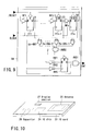
- FIG. 10 schematically shows an IC card according to an aspect of the present invention.
- An IC card 23 is, for example, one of IC cards such as wireless card and combination card, which perform data transmission/reception with respect to the wireless communication reader/writer by wireless.
- the IC card 23 For example, one is a laminate structure of laminating a plurality of plastic layers, and another is a box-type structure of covering a concave portion of a plastic substrate having the concave portion with a plastic layer.
- the IC card 23 is not limited to the above structures, in particular.
- an IC chip wireless card LSI
- an antenna 25 and a capacitor 26 are built in, and further, the IC card 23 is provided with a display section 27.
- the position of the above IC chip 24, antenna 25 and capacitor 26 in the IC card 23 is specially limited.
- the antenna 25 is arranged at part of the IC card 23; for example, it may be arranged along the edge portion of the IC card.
- the display section 27 is a novel function of the IC card 23 provided according to the present invention.
- the display section 27 displays various results relevant to data transmission/reception to the owner of the IC card. Therefore, the display section 27 has elements appealing to the owner's five senses such as eyes and ears.
- the display section 27 includes a luminous display section, a speech (voice) display section and a vibration display section.
- the luminous display section emits light (including brightness/dark, color, light emitting pattern (time, shape), etc.) so as to appeal to the owner's sense of seeing.
- the voice display section gives speech so as to appeal the owner's sense of hearing.
- the vibration display section appeals to the owner's sense of touch by vibration.
- the display section 27 is the luminous display section, the display section 27 comprises one or several LED (Light Emitting Device). For convenience of building the LED in the IC card 23, it is desirable to use a thin-type LED.
- LED Light Emitting Device
- the LED emits light.
- the owner of the IC card 23 confirms the presence of light emitting by the display section of the IC card 23. In this manner, the owner of the IC card 23 can confirm whether or not data transmission/reception is accurately carried out with respect to the wireless communication reader/writer or proper processing is performed by the data transmission/reception.
- the owner of the IC card 23 can confirm the result relevant to data transmission/reception based on the presence of light emitting by the LEDs and the light-emitting pattern (shape such as characters).
- the result relevant to data transmission/reception can be displayed on the display section by display means such as characters and graphics.
- each LED include a function of emitting light having several kinds of colors, and the display section 27 comprises several kinds of LED emitting light having different color.
- the owner of the IC card 23 can confirm the result relevant to data transmission/reception by the light color in addition to the presence of light emitting of the several LEDs and the light emitting pattern.
- the display section 27 comprises a plurality of LEDs emitting light having several kinds of colors or several kinds of LED emitting light having different color.
- the light-emitting pattern and the light color can be changed based on data registered in the non-volatile memory built in the IC card 23.
- grade information of the IC card 23 is previously registered in the non-volatile memory. Based on the grade information, the light-emitting pattern and the light color can be changed.
- pattern information character and graphic information
- color information displayed on the display section may be determined based on information registered in the non-volatile memory.
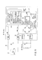
- FIG. 11 shows a display system built in the IC card of the present invention.
- the display system is configured in a manner that LED emits light when power is supplied to the IC chip from the wireless communication reader/writer via the antenna.
- the IC chip (wireless card LSI) 24 has a power supply terminal 29, a ground terminal 30 and antenna terminals 31 and 32.
- An LED 27A is connected as the display section 27 between the power-supply terminal 29 and the ground terminal 30.
- a smoothing capacitor 26 and a resistor 28 are provided for stabilizing the power.
- An antenna coil 25 and a capacitor 26 are connected in parallel between the antenna terminals 31 and 32.
- the tuning capacitor 26 is provided for tuning to a wireless communication frequency.
- the IC chip 24 is formed with a control circuit/memory section 33, rectifier circuit 34, a transmission/reception control circuit 35, a shunt regulator 36 and power stabilizing capacitor 37.
- the control circuit/memory section 33 includes memory (i.e., ROM, RAM, etc.), a non-volatile memory, a logic circuit and a transmission/reception interface circuit.
- the rectifier circuit 34 is connected between the antenna terminals 31 and 32, and rectifies an electromotive force generated in the antenna 25 so that a current can be give to transmission/reception control circuit 35.
- the transmission/reception control circuit 35 supplies a control signal to the control circuit/memory section 33 while outputting a power supply potential VDD.
- the shunt regulator 36 is provided in order to discharge electrical charges when power is too supplied from the antenna 25, to stabilize the power supply potential VDD, and to prevent heating.
- the capacitor 37 has a function of stabilizing the power-supply potential VDD.
- An output signal (power supply potential VDD) of the transmission/reception control circuit 35 is supplied to the control circuit/memory section 33 while being given to the power supply terminal 29.
- the power supply potential VDD is generated so that the LED 27a of the display section 27 can emit light.
- the IC card is additionally provided with the display function. Therefore, the owner can confirm the results below with the use of the IC card 23 when carrying out data transmission/reception with respect to the wireless communication reader/writer.
- One of the above results is determination whether or not data transmission/reception is accurately carried out with respect to the wireless communication reader/writer. Another is determination whether or not proper processing is performed by the data transmission/reception.
- the display section 27 may comprise liquid crystal and organic EL display devices in addition to LED.
- the IC card according to an aspect of the present invention is built in personal mobile information devices (PDA: Personal Digital Assistants).
- PDA Personal Digital Assistants
- the feature is that the above has a recording area for recording security information of the personal mobile information device.
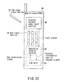
- FIG. 12 schematically shows a personal mobile information device.
- a mobile information device 38 has a key input section 39, a display screen/data input section 40, a pen type input device 41, and an operation control section 42.
- the key input section 39 can input numerical information, and inputs telephone numbers if the mobile information device has a personal identification number and a mobile phone function.
- the display screen/data input section 40 has a function of displaying character and graphic information, and a function of inputting the character and graphic information into the mobile information device 38 by using the pen type input device 41.
- the above mobile information device 38 has a function of building (loading) an IC card (e.g., SIM card) 43 therein.
- an IC card e.g., SIM card
- FIG. 13 schematically shows an IC card.
- the IC card 43 has a ROM (program stored area) 44, a non-volatile memory, a CPU 47 and a communication circuit/signal input-output section 48.
- the above non-volatile memory includes a various data area 45 and an information recording area 46 for recording character and graphic information.
- the ROM 44 stores programs for making data exchange between mobile informations devices and the IC card.
- Personal data such as User's ID number, name, age and address are registered in the various data area 45 of the non-volatile memory.
- the information recording area 46 of the non-volatile memory is an area for registering security information relevant to the present invention, and is newly provided element.
- the user in disusing the mobile information device 38, the user previously takes the IC card 43 out of the mobile information device 38. By doing so, even if the user loses the mobile information device 38 only, illegal use by another person is prevented; as a result, the user does not receive great damage.
- security effect is further improved in the IC card system shown in FIG. 12 and FIG. 13 in the following manner. That is, even in a state that the IC card 43 is inserted into the mobile information device 38, it is impossible to use the mobile information device 38 so long as predetermined conditions are not satisfied.
- the security information may be any other pattern information such as character and graphic information so long as the user can input it by the pen type input device.
- An input signal (pattern information) used as security information is registered in the information recording area 46 of the non-volatile memory via the operation control section 42.
- the user When using the mobile information device 38, the user inserts the IC card 43 into the mobile information device 38.
- the mobile information device 38 requires pattern information input to the user.
- the user inputs the pattern information from the display screen/data input section 40 using the pen type input device 41.
- the use of the mobile information device 38 is permitted when the following condition is satisfied. That is, the inputted pattern information coincides with the above pattern information (security information) registered in the information recording area 46 of the non-volatile memory of the IC card 43 with predetermined precision or more. On the contrary, the use of the mobile information device 38 is not permitted under the condition below. That is, the inputted pattern information does not coincide with the pattern information registered in the information recording area 46 with predetermined precision or more.
- the security information (pattern information) is registered in the information recording area 46 of the non-volatile memory of the IC card 43, the user can intactly use the mobile information device 38. In this case, the input of security information is not required from the mobile information device 38.
- the user can change the security information (pattern information) registered in the information recording area 46 of the non-volatile memory of the IC card 43.
- the registration area of the pattern information (security information is set to the whole or part of the display screen/data input section 40.
- n ⁇ m pixels of the registration area become all logic "1" state, and part touched by the pen type input device 41, the pixel changes from the logic "1" state to logic "0" state.
- the security information When registering the security information, "1"/"0" information (matrix data) of each pixel of the registration area, that is, pattern information is registered in the information recording area 46 of the non-volatile memory of the IC card 43 (e.g., SIM card).
- the pattern information may include other patterns such as characters and graphics.
- the CPU 47 detects the above operation. Thereafter, the CPU 47 requires the pattern information (matrix data) input to the user (input information waiting state).
- the request of pattern information input is made if all data of the information recording area 46 of the non-volatile memory of the IC card 43 are not "1" (at least one pixel is "0", that is, if security information is registered.
- the IC card 43 If the data of the information recording area 46 of the non-volatile memory of the IC card 43 are all "1", that is, if security information is not registered, the IC card immediately outputs a use permission signal to the operation control section 42.
- the user inputs the pattern information from the display screen/data input section 40 using the pen type input device 41.
- the pattern information is transferred to the IC card 43 via the operation control section 42. Unless a rewrite request is made (if a rewrite request signal is not activated), the IC card 43 compares the inputted pattern information with the pattern information (security information) already registered in the information recording area 46.
- a degree of correspondence of the inputted pattern information and the pattern information registered in the information recording area 46 is more than a predetermined value (e.g., 95%), the IC card 43 outputs a use permission signal to the operation control section 42. If the degree of correspondence of the same as above is less than the predetermined value, the IC card 43 does not output the use permission signal to the operation control section 42.
- the above inputted pattern information is given to the IC card 43 while an activated rewrite request signal being given thereto.
- the IC card 43 reregisters newly inputted pattern information in the information recording area 46 in place of the pattern information already registered.
- the use of the mobile information device 38 is not permitted so long as the following condition is not satisfied.
- the condition is the correspondence of pattern information comprising character and graphic information.
- numerical information such as personal identification number may be registered in the information recording area 46 of the non-volatile memory in place of the above pattern information such as character and graphic information.
- the numerical information is inputted from the key input section 39.
- the personal identification number is set so that it has no change from default or is hard to be anticipated.
- the IC card is provided with the following various functions.
- the functions are instantaneous blackout detecting function, display function relevant to data transmission/reception, and further, high security function.
Landscapes
- Engineering & Computer Science (AREA)
- Theoretical Computer Science (AREA)
- Computer Hardware Design (AREA)
- Physics & Mathematics (AREA)
- General Physics & Mathematics (AREA)
- Microelectronics & Electronic Packaging (AREA)
- General Engineering & Computer Science (AREA)
- Computer Security & Cryptography (AREA)
- Software Systems (AREA)
- Mathematical Physics (AREA)
- Computer Networks & Wireless Communication (AREA)
- Artificial Intelligence (AREA)
- Computer Vision & Pattern Recognition (AREA)
- Credit Cards Or The Like (AREA)
- Logic Circuits (AREA)
- Lighting Device Outwards From Vehicle And Optical Signal (AREA)
- Measurement Of Current Or Voltage (AREA)
- Power Sources (AREA)
Abstract
Description
A
Further, data held by the fillip-flop circuit FF2 is shifted to the flip-flop circuit FF1 while being held by the flip-flop circuit FF2.

Claims (30)
- An IC chip using for an IC card characterized by comprising:a CPU (19); andan instantaneous blackout detecting circuit (18) detecting a temporary step-down of a power supply potential supplied to circuits including the CPU (19), and giving information relevant to the step-down of the power supply potential to the CPU (19).
- An IC chip according to claim 1, characterized in that the CPU (19) executes predetermined interrupt handling or processing for stopping the self-operation when the power supply potential steps down.
- A multi-function IC card comprising an IC chip according to claim 1 or 2.
- An instantaneous blackout detecting circuit characterized by comprising:wherein the initial condition is set so that data of mutually adjacent two flip-flop circuits of the several flip-flop circuits (FF1, FF2, FF3, FF4, ... FFn) becomes mutually different value.a plurality of flip-flop circuits (FF1, FF2, FF3, FF4 ... FFn) connected like a ring; andlogic circuits (Ex-OR1, Ex-OR2, ... Ex-ORn-1) making an exclusive-OR operation of output signals of mutually adjacent two flip-flop circuits of said plurality of flip-flop circuits (FF1, FF2, FF3, FF4, ... FFn),
- An instantaneous blackout detecting circuit according to claim 4, characterized in that if the number of the flip-flop circuits (FF1, FF2, FF3, FF4 ... FFn) is three or more, the logic circuit includes a plurality of exclusive-OR gate circuits (Ex-OR1, Ex-OR2, ... Ex-ORn-1) and an AND gate circuit (AND2) making an AND operation of output signals of said plurality of exclusive-OR gate circuits.
- An instantaneous blackout detecting circuit according to claim 5, further comprising:an output flip-flop circuit (FFC) holding an output signal of the logic circuit.
- An instantaneous blackout detecting circuit according to claim 6, characterized in that said plurality of flip-flop circuits (FF1, FF2, FF3, FF4, ... FFn) and the output flip-flop circuit (FFC) both operate in synchronous with a clock signal, and shift occurs by a half period of the clock signal CLOCK between timing when said plurality of flip-flop circuits (FF1, FF2, FF3, FF4, ... FFn) operate and timing when the output flip-flop circuit (FFC) operates.
- An instantaneous blackout detecting circuit according to claim 7, further comprising:an AND gate circuit (AND1) making an AND operation of the clock signal and the output signal of the output flip-flop circuit (FFC).
- An IC chip comprising an instantaneous blackout detecting circuit according to claim 4, 5, 6, 7 or 8.
- A multi-function IC card comprising an IC chip according to claim 9.
- A multi-function IC card characterized by comprising:an IC chip (24) performing data processing; anda display section (27) displaying information relevant to the data transmission/reception.
- A multi-function IC card further comprising:an antenna (25) for performing the data transmission/reception by wireless.
- A multi-function IC card according to claim 11, characterized in that information relevant to the data transmission/reception includes information whether or not the data transmission/reception is accurately carried out, or whether or not proper processing is performed by the data transmission/reception.
- A multi-function IC card according to claim 11, characterized in that the display section (27) comprises a light-emitting device (27A).
- A multi-function IC card according to claim 14, characterized in that the light-emitting device (27A) emits light when power is supplied thereto via the antenna (25).
- A multi-function IC card according to claim 11, characterized in that the display section (27) comprises a plurality of light-emitting devices arranged like an array.
- A multi-function IC card according to claim 14 or 16, further comprising:a memory (33) storing information for determining a luminous pattern or color in the display section (27).
- A multi-function IC card according to claim 11, characterized in that the display section (27) is one of a luminous display section, a speech (voice) display section and a vibration display section.
- A multi-function IC card according to claim 11, characterized in that the display section (27) is one of LED and organic EL.
- A multi-function IC card according to claim 11, characterized in that the multi-function IC card (23) is a wireless card or combination card.
- A multi-function IC card using for a mobile information device characterized by comprising:an information recording area (46) recording pattern information used as security information; anda CPU (47) performing the pattern information processing.
- A multi-function IC card according to claim 21, characterized in that the information recording area (46) is provided in a non-volatile memory.
- A mobile information device characterized by comprising:a multi-function IC card (43) according to claim 21;a data input section (40) for inputting the pattern information; andan operation control section (42) controlling the operation of a device main body.
- A mobile information device according to claim 23, characterized in that the pattern information is registered in the information recording area (46) of the multi-function IC card (43) when security information is registered or changed.
- A mobile information device according to claim 23, characterized in that the multi-function IC card (43) outputs an input request of the pattern information when the device main body is used, and compares pattern information inputted from the data input section (40) with pattern information registered in the information recording area (46).
- A mobile information device according to claim 23, characterized in that the multi-function IC card (43) outputs a signal for permitting the use of the device main boy (38) if the pattern information inputted from the data input section (40) coincides with pattern information registered in the information recording area (46) with predetermined precision or more.
- A mobile information device according to claim 23, characterized in that the multi-function IC card (43) immediately outputs a signal for permitting the use of the device main boy (38) without outputting an input request of the pattern information unless the pattern information is registered in the information recording area (46).
- A mobile information device according to claim 23, characterized in that the operation control section (42) stops the operation of the device main body (38) unless the multi-function IC card (43) is inserted into the device main body (38).
- A mobile information device according to claim 23, characterized in that the pattern information includes character and graphic information.
- A mobile information device according to claim 23, characterized in that the multi-function IC card (43) is a SIM card.
Applications Claiming Priority (2)
| Application Number | Priority Date | Filing Date | Title |
|---|---|---|---|
| JP2001388277A JP3848152B2 (en) | 2001-12-20 | 2001-12-20 | Multifunctional IC card |
| JP2001388277 | 2001-12-20 |
Publications (2)
| Publication Number | Publication Date |
|---|---|
| EP1321845A2 true EP1321845A2 (en) | 2003-06-25 |
| EP1321845A3 EP1321845A3 (en) | 2010-02-24 |
Family
ID=19188129
Family Applications (1)
| Application Number | Title | Priority Date | Filing Date |
|---|---|---|---|
| EP02028737A Withdrawn EP1321845A3 (en) | 2001-12-20 | 2002-12-20 | Multi-function IC card |
Country Status (6)
| Country | Link |
|---|---|
| US (1) | US7126371B2 (en) |
| EP (1) | EP1321845A3 (en) |
| JP (1) | JP3848152B2 (en) |
| KR (1) | KR100560028B1 (en) |
| CN (1) | CN1241092C (en) |
| TW (1) | TW200305106A (en) |
Cited By (2)
| Publication number | Priority date | Publication date | Assignee | Title |
|---|---|---|---|---|
| DE102005052070A1 (en) * | 2005-10-28 | 2007-05-03 | Bundesdruckerei Gmbh | display device |
| WO2014005995A1 (en) * | 2012-07-04 | 2014-01-09 | Fujitsu Technology Solutions Intellectual Property Gmbh | Computer system and method for operating a computer system |
Families Citing this family (9)
| Publication number | Priority date | Publication date | Assignee | Title |
|---|---|---|---|---|
| FR2875311A1 (en) * | 2004-09-14 | 2006-03-17 | St Microelectronics Sa | METHOD FOR DETECTING THE RELATIVE POSITIONING OF TWO SIGNALS AND CORRESPONDING DEVICE |
| JP4810108B2 (en) * | 2005-03-04 | 2011-11-09 | 株式会社東芝 | IC card and control method thereof |
| US7622961B2 (en) * | 2005-09-23 | 2009-11-24 | Intel Corporation | Method and apparatus for late timing transition detection |
| JP4420932B2 (en) * | 2007-03-09 | 2010-02-24 | 株式会社沖データ | Flexible display body and article with flexible display body |
| JP2009147221A (en) * | 2007-12-17 | 2009-07-02 | Renesas Technology Corp | Semiconductor device |
| US10502784B2 (en) * | 2017-09-22 | 2019-12-10 | Stmicroelectronics International N.V. | Voltage level monitoring of an integrated circuit for production test and debug |
| CN112910491B (en) * | 2021-01-28 | 2022-08-02 | 维沃移动通信有限公司 | Terminal double-card communication method, device, equipment and storage medium |
| TWI781844B (en) * | 2021-12-07 | 2022-10-21 | 莊連豪 | Trading card with illuminated display |
| US12413233B1 (en) | 2025-06-03 | 2025-09-09 | Kuwait University | 4-bit synchronous counter IC with ripple carry-out, loading capability, and integrated MOD-10 reset functionality |
Family Cites Families (11)
| Publication number | Priority date | Publication date | Assignee | Title |
|---|---|---|---|---|
| IT1241429B (en) * | 1990-03-01 | 1994-01-17 | Sip | ELECTRONIC CIRCUIT FOR THE GENERATION OF CODES FOR DETECTION OF ERRORS IN NUMERICAL SIGNALS |
| JPH06282600A (en) * | 1993-03-29 | 1994-10-07 | Mitsubishi Electric Corp | Logic simulation device |
| WO1995004402A1 (en) * | 1993-08-03 | 1995-02-09 | Xilinx, Inc. | Microprocessor-based fpga |
| US5761446A (en) * | 1995-06-14 | 1998-06-02 | Unisys Corp | Livelock avoidance |
| JP3720878B2 (en) | 1995-08-10 | 2005-11-30 | 大日本印刷株式会社 | IC card |
| JP3493096B2 (en) | 1996-06-07 | 2004-02-03 | 株式会社東芝 | Semiconductor integrated circuit, IC card, and IC card system |
| TW420788B (en) | 1998-03-06 | 2001-02-01 | Mass Rich Internat Dev Ltd | Display type IC card |
| EP0964360B1 (en) * | 1998-06-08 | 2003-08-27 | International Business Machines Corporation | Automatic data recovery of integrated circuit cards |
| US6072849A (en) * | 1998-08-04 | 2000-06-06 | Vlsi Technology, Inc. | Shift counter device |
| US6469549B2 (en) * | 2000-11-30 | 2002-10-22 | Infineon Technologies Ag | Apparatus and method for odd integer signal division |
| JP2002251227A (en) * | 2001-02-23 | 2002-09-06 | Nec Microsystems Ltd | Clock monitoring circuit, data processor and data processing system |
-
2001
- 2001-12-20 JP JP2001388277A patent/JP3848152B2/en not_active Expired - Fee Related
-
2002
- 2002-12-13 TW TW091136092A patent/TW200305106A/en not_active IP Right Cessation
- 2002-12-18 KR KR1020020081188A patent/KR100560028B1/en not_active Expired - Fee Related
- 2002-12-20 CN CNB021611211A patent/CN1241092C/en not_active Expired - Fee Related
- 2002-12-20 EP EP02028737A patent/EP1321845A3/en not_active Withdrawn
- 2002-12-20 US US10/327,513 patent/US7126371B2/en not_active Expired - Fee Related
Cited By (3)
| Publication number | Priority date | Publication date | Assignee | Title |
|---|---|---|---|---|
| DE102005052070A1 (en) * | 2005-10-28 | 2007-05-03 | Bundesdruckerei Gmbh | display device |
| WO2014005995A1 (en) * | 2012-07-04 | 2014-01-09 | Fujitsu Technology Solutions Intellectual Property Gmbh | Computer system and method for operating a computer system |
| US9933839B2 (en) | 2012-07-04 | 2018-04-03 | Fujitsu Technology Solutions Intellectual Property Gmbh | Computer system and method of operating a computer system |
Also Published As
| Publication number | Publication date |
|---|---|
| KR20030053019A (en) | 2003-06-27 |
| JP2003187202A (en) | 2003-07-04 |
| US20040078661A1 (en) | 2004-04-22 |
| CN1474354A (en) | 2004-02-11 |
| KR100560028B1 (en) | 2006-03-15 |
| TW200305106A (en) | 2003-10-16 |
| US7126371B2 (en) | 2006-10-24 |
| TWI292128B (en) | 2008-01-01 |
| EP1321845A3 (en) | 2010-02-24 |
| JP3848152B2 (en) | 2006-11-22 |
| CN1241092C (en) | 2006-02-08 |
Similar Documents
| Publication | Publication Date | Title |
|---|---|---|
| US7126371B2 (en) | Multi-function IC card | |
| EP0595305B1 (en) | IC card reader | |
| EP0964360B1 (en) | Automatic data recovery of integrated circuit cards | |
| US7270276B2 (en) | Multi-application smartcard | |
| US7779192B2 (en) | Electronic device with card interface | |
| US20080185444A1 (en) | Multi-Mode Integrated Circuit Devices Including Mode Detection and Methods of Operating the Same | |
| US20020103944A1 (en) | Arrangement with a microprocessor | |
| KR100619213B1 (en) | Dual Interface IC Card | |
| US11983587B2 (en) | Biometric interface | |
| CN112445371A (en) | Sensing panel and display device | |
| WO2013120826A1 (en) | Battery management scheme for nfc | |
| CN1763772A (en) | IC cards for reduced power consumption | |
| KR100798682B1 (en) | Smart card | |
| US20070293154A1 (en) | Data exchange systems and methods employing RF data transmission | |
| WO2001028782A1 (en) | Electronic name card | |
| KR101075177B1 (en) | Smartcard with Keypad | |
| CN223796944U (en) | Electronic equipment | |
| US20100164682A1 (en) | Ic card, data control method and program | |
| KR20080064406A (en) | Smart card showing balance | |
| JP3263867B2 (en) | IC card detection method | |
| KR20250055471A (en) | Biometric system on card and method for controlling the same | |
| JP2002251593A (en) | Non-contact type ic card and usage of it | |
| US8521935B2 (en) | Portable electronic apparatus, control method for portable electronic apparatus, and IC card | |
| JP2023082497A (en) | ELECTRONIC INFORMATION STORAGE MEDIUM, IC CHIP, LIGHT-EMITTING METHOD, AND PROGRAM | |
| WO2006085300A2 (en) | A security card apparatus |
Legal Events
| Date | Code | Title | Description |
|---|---|---|---|
| PUAI | Public reference made under article 153(3) epc to a published international application that has entered the european phase |
Free format text: ORIGINAL CODE: 0009012 |
|
| 17P | Request for examination filed |
Effective date: 20021220 |
|
| AK | Designated contracting states |
Designated state(s): AT BE BG CH CY CZ DE DK EE ES FI FR GB GR IE IT LI LU MC NL PT SE SI SK TR |
|
| AX | Request for extension of the european patent |
Extension state: AL LT LV MK RO |
|
| PUAL | Search report despatched |
Free format text: ORIGINAL CODE: 0009013 |
|
| AK | Designated contracting states |
Kind code of ref document: A3 Designated state(s): AT BE BG CH CY CZ DE DK EE ES FI FR GB GR IE IT LI LU MC NL PT SE SI SK TR |
|
| AX | Request for extension of the european patent |
Extension state: AL LT LV MK RO |
|
| 17Q | First examination report despatched |
Effective date: 20100419 |
|
| AKX | Designation fees paid |
Designated state(s): DE FR GB |
|
| STAA | Information on the status of an ep patent application or granted ep patent |
Free format text: STATUS: THE APPLICATION IS DEEMED TO BE WITHDRAWN |
|
| 18D | Application deemed to be withdrawn |
Effective date: 20100831 |