TECHNICAL FIELD
The present invention relates to an electronic
timepiece having a function for generating function
information and warning information besides watch
information and a control method for the electronic
timepiece.
BACKGROUND ART
Among modern electronic timepieces, electronic
timepieces that have therein systems for displaying a
plurality of kinds of functions, including a
chronographic display function, alarm display function,
atmospheric pressure display function, sounding display
function, temperature display function, etc. have
started to be put to practical use, and are configured
so that one or a plurality of kinds of function
information is displayed simultaneously with or
alternatively to time information on specific display
means.
Conventionally, on the other hand, some known
electronic timepieces additionally have a power-saving
mode function that serves to lower the power
consumption of the electronic timepiece unless it
constitutes any special hindrance to the use of the
electronic timepiece, in order to maximize the
durability of power source means that is composed of a
battery or an accumulator used in combination with
power generating means.
As is described in Japanese Patent Application
Laid-Open No. 61-77788, for example, an electronic
timepiece is known that has a solar cell as its main
power source and is constructed so that a power-saving
mode is established to lower its power consumption if
the sunlight is not incident upon a solar cell of the
electronic timepiece for a predetermined fixed
continuous time, and that the power-saving mode is
canceled when the sunlight is incident again upon the
solar cell.
The power-saving mode function of this
conventional electronic timepiece is designed so that
the power-saving mode is established to stop the
display of time information if the power source is in
an unfavorable situation or if the solar cell as the
power source is used in the dark, for example.
Although both the power-saving mode function and
the function information operation state mode serve to
improve the commercial value of the electronic
timepiece, they may possibly interfere with each other,
so that the drive of the respective operations of the
two functions requires adjustment.
If the display function for function information
is activated when the environment of power generation
or the level of charge is lowered, for example, the
battery is consumed by power that is required by the
display of the function information, so that the
original time display function of the electronic
timepiece may possibly be stopped.
Further, some known rechargeable electronic
timepieces are designed so that information on the
state of the power source of the watch and the past
history of stoppage can be given to a user of the watch
and that trouble caused as the watch run-down due to
undercharge can be avoided to the utmost. Described in
Japanese Patent Application Laid-Open No. 62-194484,
for example, is an electronic timepiece, in which
normal operation (one-second-step movement) is
performed if the charge level (supply voltage) of the
power source is adequate, first modulated hand movement
operation (two-second-step movement) as a charge
warning is performed if the charge level is about to
fail, and second modulated hand movement operation as a
run-down state warning, modulated differently from the
first modulated hand movement operation, is performed
to warn the user of the past history of a run-down
state (and therefore, wrongness of indicated time)
despite later recovery of the charge level and restart
of the hand movement if the charge level is so low that
the watch is stopped, whereby two types of warning
display are performed. Also known is an electronic
timepiece that performs residue warning information
display such that the residual capacity (residue) of a
battery is indicated by the movement of a pointer.
Described in Japanese Patent Application Laid-Open No.
55-22153, for example, is an electronic timepiece that
displays residue warning information in accordance with
the movement of a pointer in a residue warning display
monitor mode based on switch operation.
If the hand movement operation is stopped so that
the display is stopped in a power-saving state, warning
information also ceases to be displayed, so that the
electronic timepiece inevitably cannot fulfill its
function, as in the case of the aforementioned
invention described in Japanese Patent Application
Laid-Open No. 61-77788. The warning information, in
particular, is information that is related to the state
of the power source, and is generated when the supply
voltage is lowered if accumulator means is undercharged
by power generating means. The same applies to the
aforementioned residue warning display of Japanese
Patent Application Laid-Open No. 55-22153. Further, the
power-saving function, especially in a rechargeable
electronic timepiece, is a function that is required
when the accumulator means is undercharged. The warning
display is needed with high possibility in a state that
requires power-saving operation.
Accordingly, a first object of the present
invention is to provide an electronic timepiece having
both of functions for function display operation and
power-saving operation and a driving method for the
electronic timepiece, and to provide an electronic
timepiece with high commercial value, which is
configured to be able to use separately a power-saving
mode function that entails lower power consumption and
a function information operation state mode that
provides many kinds of additional function information,
and a driving method for the electronic timepiece.
Further, a second object of the present invention
is to provide an electronic timepiece, in which display
of a power-saving state and warning information is
optimally controlled so that the electronic timepiece
can fulfill its function, and a control method therefor.
DISCLOSURE OF THE INVENTION
A first form of an electronic timepiece according
to the present invention comprises time information
generating means for generating time information,
information generating means for generating information
(e.g., function information, warning information, etc.)
other than the time information, display means capable
of alternatively displaying the time information and/or
the other information, power-saving operation means for
operating the electronic timepiece in a power-saving
operation state entailing lower power consumption than
in a normal operation state, and preferential operation
selecting means for preferentially operating the
information generating means or the power-saving
operation means according to circumstances. The
individual means are driven by a power source unit.
Accumulator means such as a primary battery or a
secondary battery or power generating means and
accumulator means to be charged by the power generating
means can be used as the power source unit.
Further, a second form of the electronic
timepiece according to the present invention comprises
time information generating means for generating time
information, function information generating means for
generating function information, warning information
generating means for generating warning information for
prompting a predetermined warning, display means.
capable of alternatively displaying the time
information and/or the function information and/or the
warning information, power-saving operation means for
operating the electronic timepiece in a power-saving
operation state entailing lower power consumption than
in a normal operation state, and preferential operation
selecting means for preferentially operating the
function information generating means and/or the
warning information generating means or the power-saving
operation means according to circumstances. The
individual means are driven by a power source unit.
The electronic timepiece according to the present
invention can have the following form.
In a situation where the preferential operation
selecting means causes the function information
generating means or the warning information generating
means to operate with priority over the power-saving
operation means, the warning information generating
means is further operated with priority over the
function information generating means.
The electronic timepiece further comprises
residual capacity detecting means for detecting the
residual capacity of the accumulator means, and the
preferential operation selecting means, based on
residual capacity detection information from the
residual capacity detecting means, causes the
information generating means to operate with priority
over the power-saving operation means if the detected
residual capacity is not lower than a predetermined
value and, on the other hand, causes the power-saving
operation means to operate with priority over the
information generating means if the detected residual
capacity is lower than the predetermined value.
The electronic timepiece further comprises power
generation detecting means for detecting the power
generating state of the power generating means, and the
preferential operation selecting means, based on power
generation detection information from the power
generation detecting means, causes the information
generating means to operate with priority over the
power-saving operation means if the detected power
generating state is not lower than a predetermined
power generation level and, on the other hand, causes
the power-saving operation means to operate with
priority over the information generating means if the
detected power generating state is lower than the
predetermined power generation level.
The electronic timepiece further comprises
residual capacity detecting means for detecting the
residual capacity of the accumulator means and power
generation detecting means for detecting the power
generating state of the power generating means, and the
preferential operation selecting means, based on
residual capacity detection information from the
residual capacity detecting means and power generation
detection information from the power generation
detecting means, causes the information generating
means to operate with priority over the power-saving
operation means if the detected residual capacity is
not lower than a predetermined value and also if the
detected power generating state is not lower than a
predetermined power generation level and, on the other
hand, causes the power-saving operation means to
operate with priority over the information generating
means if the detected residual capacity is lower than
the predetermined value or if the detected power
generating state is lower than the predetermined power
generation level.
The electronic timepiece further comprises
residual capacity detecting means for detecting the
residual capacity of the accumulator means and power
generation detecting means for detecting the power
generating state of the power generating means, and the
preferential operation selecting means, based on
residual capacity detection information from the
residual capacity detecting means and power generation
detection information from the power generation
detecting means, causes the information generating
means to operate with priority over the power-saving
operation means if the detected residual capacity is
not lower than a predetermined value or if the detected
power generating state is not lower than a
predetermined power generation level and, on the other
hand, causes the power-saving operation means to
operate with priority over the information generating
means if the detected residual capacity is lower than
the predetermined value and also if the detected power
generating state is lower than the predetermined power
generation level.
The residual capacity detecting means detects the
output voltage or output current of the accumulator
means.
The power generation detecting means detects the
quantity of generated electricity, power generation
voltage, or power generation current of the power
generating means.
The display of warning information by the warning
information generating means is given priority over the
operation of the function information generating means
and the operation of the power-saving means.
The display of warning information by the warning
information generating means is given priority over the
operation of the function information generating means
and the operation of the power-saving means.
The function information generating means or the
power-saving means is not operated even if conditions
for the operation of the function information
generating means or the power-saving means are met
during the display of the warning information.
The operation of the function information
generating means or the operation of the power-saving
means is stopped and the warning information generating
means is operated to display the warning information if
conditions for the operation of the warning information
generating means are met during the operation of the
function information generating means or the operation
of the power-saving means.
Display means for displaying the function of the
function information generating means when the same is
operated or display means for stopping the display when
the power-saving means is operated and display means
for displaying the warning information when the warning
information generating means is operated are configured
to be duplicate at least partially.
The warning information is time adjustment
warning information for warning of wrong time
indication when the electronic timepiece temporarily
undercharged and stopped is restarted by recharge,
charge warning information as a warning for prompting
charge, or residue warning information as a residue
warning for the accumulator means.
At least a part of the display means is composed
of a digital display system or an analog display system.
A power source for driving each means of the
electronic timepiece is selected from power generating
means including a solar cell, windup generator, self-winding
generator, and temperature-difference generator,
or a combination of the power generating means and
accumulator means such as a secondary battery or a
high-capacity condenser.
The electronic timepiece further comprises
selecting means for causing the preferential operation
selecting means to select the preferential operation,
the selecting means being adapted to cause the
preferential operation selecting means to select the
preferential operation at the request of a user.
A first form of a control method for an
electronic timepiece according to the present invention
is a control method for an electronic timepiece
comprising time information generating means for
generating time information, warning information
generating means for generating warning information for
prompting a predetermined warning, function information
generating means for generating function information,
display means capable of alternatively displaying the
time information and/or the function information and/or
the warning information, power-saving operation means
for operating the electronic timepiece in a power-saving
operation state entailing lower power
consumption than in a normal operation state, and a
power source unit for driving the individual means. The
method is characterized in that the function
information generating means and/or the warning
information generating means or the power-saving means
is caused to perform the preferential operation
according to circumstances.
The warning information generating means may be
configured further to be operated with priority over
the function information generating means in a
situation where the preferential operation selecting
means causes the function information generating means
or the warning information generating means to operate
with priority over the power-saving operation means.
The preferential operation may be selected in
accordance with the output voltage and/or output
current of the power source unit.
The preferential operation may be selected at the
request of a user.
A second form of the control method for an
electronic timepiece according to the present invention
is a control method for an electronic timepiece
comprising reference signal generating means, general
information generating means for generating general
information such as time information or function
information in response to a reference signal from the
reference signal generating means, warning information
generating means for generating warning information for
prompting a predetermined warning, display drive means
for outputting a drive signal for displaying the
warning information and the general information, and
display means for displaying the general information
and the warning information in response to the drive
signal from the display drive means, and can assume a
power-saving state entailing lower power consumption
than in a normal operation state. The method is
characterized in that the display of the warning
information based on the operation of the warning
information generating means is given priority over the
operation of the power-saving operation means.
A third form of the control method for an
electronic timepiece according to the present invention
is a control method for an electronic timepiece
comprising reference signal generating means, general
information generating means for generating general
information such as time information or function
information in response to a reference signal from the
reference signal generating means, warning information
generating means for generating warning information for
prompting a predetermined warning, display drive means
for outputting a drive signal for displaying the
warning information and the general information, and
display means for displaying the general information
and the warning information in response to the drive
signal from the display drive means, and can assume a
power-saving state entailing lower power consumption
than in a normal operation state. The method is
characterized in that the power-saving state is not
established even if conditions for the establishment of
the power-saving state are met during the display of
the warning information by the warning information
generating means.
A fourth form of the control method for an
electronic timepiece according to the present invention
is a control method for an electronic timepiece
comprising reference signal generating means, general
information generating means for generating general
information such as time information or function
information in response to a reference signal from the
reference signal generating means, warning information
generating means for generating warning information for
prompting a predetermined warning, display drive means
for outputting a drive signal for displaying the
warning information and the general information, and
display means for displaying the general information
and the warning information in response to the drive
signal from the display drive means, and can assume a
power-saving state entailing lower power consumption
than in a normal operation state. The power-saving
state is canceled to establish a display state for the
warning information if conditions for the operation of
the warning information generating means are met during
the power-saving state.
BRIEF DESCRIPTION OF THE DRAWINGS
FIG. 1 is a diagram for illustrating a first
operation example of a first embodiment of an
electronic timepiece according to the present
invention;
FIG. 2 is a diagram for illustrating a second
operation example of the first embodiment of the
electronic timepiece according to the present
invention;
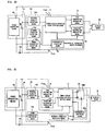
FIG. 3 is a schematic block diagram showing a
configuration example of the electronic timepiece
corresponding to the operation example of FIG. 1;
FIG. 4 is a schematic block diagram showing a
configuration example of the electronic timepiece
corresponding to the operation example of FIG. 2;
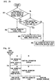
FIG. 5 is a flowchart for illustrating general
operation for preferential selection of the electronic
timepiece;
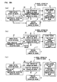
FIG. 6 is a diagram for illustrating power-saving-first
operation and function-first operation;
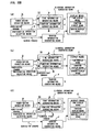
FIG. 7 is a diagram for illustrating the power-saving-first
operation and the function-first
operation;
FIG. 8 is a diagram illustrating a first
configuration example for realizing a first selection
mode of the electronic timepiece;
FIG. 9 is a diagram illustrating a second
configuration example for realizing the first selection
mode of the electronic timepiece;
FIG. 10 is a flowchart illustrating the operation
of the electronic timepiece;
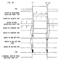
FIG. 11 is a voltage diagram illustrating
operation in the first selection mode of the electronic
timepiece;
FIG. 12 is a diagram illustrating a first
configuration example for realizing a second selection
mode of the electronic timepiece;
FIG. 13 is a diagram illustrating a second
configuration example for realizing the second
selection mode of the electronic timepiece;
FIG. 14 is a flowchart illustrating operation in
the second selection mode of the electronic timepiece;
FIG. 15 is a voltage diagram illustrating the
operation in the second selection mode of the
electronic timepiece;
FIG. 16 is a diagram illustrating a first
configuration example for realizing a third selection
mode of the electronic timepiece;
FIG. 17 is a diagram illustrating a second
configuration example for realizing the third selection
mode of the electronic timepiece;
FIG. 18 is a flowchart illustrating operation in
the third selection mode of the electronic timepiece;
FIG. 19 is a voltage diagram illustrating the
operation in the third selection mode of the electronic
timepiece;
FIG. 20 is a diagram illustrating a first
configuration example for realizing a fourth selection
mode of the electronic timepiece;
FIG. 21 is a diagram illustrating a second
configuration example for realizing the fourth
selection mode of the electronic timepiece;
FIG. 22 is a flowchart illustrating operation in
the fourth selection mode of the electronic timepiece;
FIG. 23 is a voltage diagram illustrating the
operation in the fourth selection mode of the
electronic timepiece;
FIG. 24 is a diagram illustrating a first
configuration example for realizing a fifth selection
mode of the electronic timepiece;
FIG. 25 is a diagram illustrating a second
configuration example for realizing the fifth selection
mode of the electronic timepiece;
FIG. 26 is a flowchart illustrating operation in
the fifth selection mode of the electronic timepiece;
FIG. 27 is an external operation selection and
voltage diagram illustrating the operation in the fifth
selection mode of the electronic timepiece;
FIG. 28 is a diagram showing a block
configuration example of the electronic timepiece to be
realized by software;
FIG. 29 is an external front view of the
electronic timepiece according to the present
embodiment;
FIGS. 30A and 30B are diagrams for illustrating
examples of operation of a second embodiment of the
electronic timepiece according to the present
invention;
FIG. 31 is a block diagram showing the principal
part of a first example of the second embodiment of the
electronic timepiece according to the present
invention;
FIG. 32 is a detailed block diagram of power-saving
state control means of the electronic timepiece
of FIG. 31;
FIG. 33 is a timing chart showing the operation
timing of the power-saving state control means;
FIG. 34 is a block diagram showing the principal
part of a second example of the second embodiment of
the electronic timepiece according to the present
invention;
FIG. 35 is a flowchart showing a display
switching process that a processor of an analog
electronic timepiece control device of the second
example having a CPU executes;
FIG. 36 is a block diagram showing the principal
part of a third example of the second embodiment of the
electronic timepiece according to the present
invention;
FIG. 37 is a diagram showing examples of display
by a digital display device of third and fourth
examples;
FIG. 38 is a block diagram showing the principal
part of a fourth example of the second embodiment of
the electronic timepiece according to the present
invention;
FIG. 39 is a flowchart showing a display
switching process that a processor of a digital
electronic timepiece control device of the fourth
example having a CPU executes;
FIG. 40 is a block diagram illustrating an analog
configuration and operation for giving priority to time
adjustment warning function information, charge warning
function information, etc. over a power-saving
function;
FIG. 41 is a timing chart showing warning
function display drive signals for the time adjustment
warning function information, charge warning function
information, etc.;
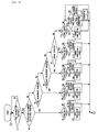
FIG. 42 is a flowchart illustrating the operation
of an analog configuration for giving priority to
various warning function states such as residual
capacity warning function information, as well as the
time adjustment warning function information and the
charge warning function information, over the power-saving
function;
FIG. 43 is a flowchart for illustrating an
operation example of a subroutine 1 of the flowchart of
FIG. 42;
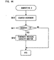
FIG. 44 is a flowchart for illustrating an
operation example of a subroutine 2 of the flowchart of
FIG. 42; and
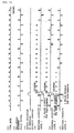
FIG. 45 is a timing chart showing warning
function display drive signals for the residual
capacity warning function information, in addition to
those for time adjustment warning function information
and the charge warning function information, and'
residual capacity monitor control.
BEST MODE FOR CARRYING OUT THE INVENTION
A first embodiment of the present invention will
be described with reference to FIGS. 1 to 29.
In this embodiment, an electronic timepiece
comprises power-saving means, function information
generating means, and preferential operation selecting
means for selecting one of these means and urging it to
perform preferential operation. When the preferential
operation selecting means selects the power-saving
operation means, it causes the power-saving operation
means to perform preferential operation to establish a
power-saving operation state without operating the
function information generating means if conditions for
power-saving operation are met. When the preferential
operation selecting means selects the function
information generating means, on the other hand, it
causes the function information generating means to
operate, and displays function information on display
means, taking preference over the power-saving
operation state, even if the conditions for the
operation of the power-saving operation means are met.
FIGS. 1 and 2 are diagrams for illustrating the
operation of the present embodiment, in which FIG. 1
shows a first example, and FIG. 2 shows a second
example.
In the first example, the power-saving operation
state or a functional operation state is given priority
by selecting and actuating any one of the power-saving
operation means and the function information generating
means by the preferential operation selecting means. In
the second example, the power-saving operation state or
the functional operation state is given priority by
controlling the drive of the power-saving operation
means by the preferential operation selecting means to
activate the power-saving operation state or inactivate
the power-saving operation, thereby enabling the
functional operation.
The first example will be described first.
In FIG. 1(a), an electronic timepiece 10
comprises time information generating means A for
generating time information, function information
generating means B for generating function information,
display means C capable of alternatively displaying the
time information and the function information, power-saving
operation means D for operation in the power-saving
operation state that entails lower power
consumption than a normal operation state, and
preferential operation selecting means E for giving
priority to any one of the function information
generating means B and the power-saving operation means
D.
In the normal operation state, as shown in FIG.
1(b), the preferential operation selecting means E does
not give priority to any of the means B and D, and the
display means C continually displays the time
information and selectively displays the function
information.
If the power-saving operation state is
established in the normal operation state or in a state
where the power-saving operation means D is given
priority by the preferential operation selecting means
E, as shown in FIG. 1(c), on the other hand, the power-saving
operation means D gives priority to the power-saving
operation over function information display
operation, and stops the display of the time
information and the function information. Depending on
the conditions for the power-saving operation, the
display of the function information can be stopped with
a part of the time information displayed, as shown in
FIG. 1(d). In display stop operation for the time
information and/or the function information, moreover,
counting the time information and the function
information can be continued.
If the function information generating means B is
given priority by the preferential operation selecting
means E, as shown in FIG. 1(e), furthermore, the
function information is displayed without regard to the
performance of the power-saving operation.
Next, the second example will be described.
In FIG. 2(a), an electronic timepiece 10
comprises time information generating means A for
generating time information, function information
generating means B for generating function information,
display means C capable of alternatively displaying the
time information and the function information, power-saving
operation means D for operation in the power-saving
operation state that entails lower power
consumption than a normal operation state, and
preferential operation selecting means E for
controlling the power-saving operation means D to give
priority to the power-saving operation or the
functional operation.
In the normal operation state, the preferential
operation selecting means E does not give priority any
of the power-saving and functional operations, the
power-saving operation means D does not function, and
the display means C continually displays the time
information and selectively displays the function
information, as shown in FIG. 2(b). If the power-saving
operation state is established in the normal operation
state or in a state where the power-saving operation
means D is given priority by the preferential operation
selecting means E, as shown in FIG. 2(c), on the other
hand, the power-saving operation means D gives priority
to the power-saving operation over function information
display operation, and stops the display of the time
information and the function information. Depending on
the conditions for the power-saving operation, the
display of the function information can be stopped with
the time information displayed, as shown in FIG. 2(d).
In display stop operation for the time information
and/or the function information, moreover, counting the
time information and the function information can be
continued.
If the functional operation is given priority by
the preferential operation selecting means E, as shown
in FIG. 2(e), furthermore, the function information is
displayed without regard to the performance of the
power-saving operation.
Thus, in the present embodiment, the electronic
timepiece is provided with both a function to make the
consumption period of a battery as long as possible by
driving as many power-savable parts as possible in a
power-saving mode and an additional function for
improving the commercial value of the electronic
timepiece, and is designed so that the power-saving
operation state and the functional operation state can
be alternatively selected according to the power supply
condition of the electronic timepiece or a user's
request. If the power-saving operation is esteemed, the
power-saving operation state is given priority over the
function display operation state. If the functional
operation is esteemed, the function display operation
state is given priority over the power-saving operation
state.
Objective parts to be brought to the power-saving
operation state are parts that require the
establishment of the power-saving operation state or
the function display operation state, depending on
various environments such as the working conditions and
the purpose of use of the electronic timepiece. These
objective parts include display means, such as hour,
minute, and second hands or a liquid crystal notation
device, and all or some of associated circuit elements
for controlling them. Those circuit elements include,
for example, drive circuit elements of various display
means.
The display means of the electronic timepiece of
the present embodiment may include all or some of
display means that belong to the electronic timepiece
and can include display means associated with function
display. Those display means which are not associated
with function display can be constructed in a manner
such that the power-saving mode is started when the
quantity of electricity generated by power generating
means is lowered, without regard to the performance of
the function display operation.
An example of configuration of the electronic
timepiece of the present embodiment and a driving
method for the electronic timepiece will now be
described in detail with reference to the drawings.
In the description of the configuration example
to follow, the display means (hour, minute, and second
hands, functional hand, or liquid crystal display) is
used as an object for which the power-saving operation
state or the functional operation state is realized. It
is to be understood, however, that this display means
is nothing but an example according to the present
embodiment, and is included in the present embodiment
only if it is a circuit element that can realize the
power-saving operation state or the functional
operation state.
FIGS. 3 and 4 are schematic block diagrams for
illustrating configuration examples of the electronic
timepiece 10 according to the present embodiment. The
configuration example of FIG. 3 corresponds to the
example of operation shown in FIG. 1, and the
configuration example of FIG. 4 to the example of
operation shown in FIG. 2.
In FIGS. 3 and 4, the electronic timepiece 10
comprises reference signal generating means 1, time
information generating means 2 for generating time
information TJ in response to a reference signal SR
from the reference signal generating means 1, function
information generating means 3 for generating function
information FJ, display drive means 4 for outputting
drive signals DRF and DRT for displaying the function
information FJ and the time information TJ on a display
means, display means 5 for displaying the function
information FJ and the time information TJ in response
to the drive signals DRF and DRT, a power source 6,
power-saving operation state detecting means 7, and
control means 8.
Further, the electronic timepiece 10 comprises
preferential operation selecting means 9 for giving
priority to the power-saving operation or the
functional operation, whereby the power-saving
operation state that entails lower power consumption
than the normal operation state can be realized.
Furthermore, the electronic timepiece 10 shown in
FIGS. 3 and 4 comprises power-saving operation state
setting means 11 for carrying out the power-saving
operation, functional operation state setting means 12
for carrying out the functional operation, and the
preferential operation selecting means 9 for
preferentially operating the power-saving operation
state setting means 11 or the functional operation
state setting means 12.
In the configuration example of FIG. 3, the
power-saving operation state setting means 11 is means
for setting the time information generating means 2
and/or the function information generating means 3 in
the power-saving operation state in response to a
detection signal SAD from the power-saving operation
state detecting means 7. The functional operation state
setting means 12 is means for setting the function
information generating means 3 in the functional
operation state, and is set in accordance with a
control signal (broken line in the drawing) from the
control means 8. Further, any one of the power-saving
operation state setting means 11 and the functional
operation state setting means 12 is preferentially set
in response to a selection signal from the preferential
operation selecting means 9, and the time information
generating means 2 or the function information
generating means 3 to which only the preferentially set
setting means corresponds is allowed to operate.
In the configuration example of FIG. 3, therefore,
any one of the power-saving operation and the
functional operation is preferentially performed by
controlling the permission of the operation of the time
information generating means 2 or the function
information generating means 3 by the preferential
operation selecting means 9.
In the configuration example of FIG. 4, on the
other hand, the power-saving operation state setting
means 11 is means for setting at least a part of the
display means, e.g., at least a part of time
information display means 5a and/or at least a part of
function information display means 5b, in the power-saving
operation state in response to the detection
signal SAD from the power-saving operation state
detecting means 7. Further, the functional operation
state setting means 12 is means for setting at least a
part of function information display means 5b in the
functional operation state in response to a detection
signal FUD from functional operation state detecting
means 13. The preferential selection of the respective
operations of the aforesaid individual means is set in
accordance with the control signal (broken line in the
drawing) from the control means 8.
Further, the power-saving operation state setting
means 11 or the functional operation state setting
means 12 is preferentially set in response to the
selection signal from the preferential operation
selecting means 9, and the time information generating
means 2 or the function information generating means 3
to which only the preferentially set setting means
corresponds is allowed to operate. In the drawing, 11a
denotes power-saving operation state setting means for
time display means, and 11b denotes power-saving
operation state setting means for function information
display means.
In the configuration example of FIG. 4, therefore,
any one of the power-saving operation and the
functional operation is preferentially performed by
controlling the permission of operation for causing
display means to display information generated in the
time information generating means 2 and/or the function
information generating means 3, by the preferential
operation selecting means 9.
In the configuration example described above, the
time information display means 5a and the function
information display means 5b are composed of separate
circuits, in some cases. In other cases, they are
partially or wholly overlapped. During chronographic
display by the function information display means 5b, a
second hand 23 (FIG. 29) of the time information
display means 5a in the normal operation state, for
example, may be used overlapped as means for displaying
chronographic seconds, in some cases.
The flowchart of FIG. 5 shows an outline of the
operation for preferential selection of the electronic
timepiece of the present embodiment. The functional
operation or the power-saving operation is selected by
the preferential operation selecting means 9 (Step S1).
If the functional operation is requested (Step
S2) when the functional operation is selected (Step S1),
function information is displayed on the display means
(Step S3). Even if power-saving conditions are met
(Step S4) owing to a drop of the supply voltage or the
like when the functional operation is preferentially
selected (Step S4), the power-saving operation is
cancelled (Step S5) since the functional operation is
given priority.
If the power-saving conditions are met owing to a
drop of the supply voltage or the like when the power-saving
operation is selected (Step S6), on the other
hand, power-saving operation, such as stopping
displaying the time information on the display means 5,
is performed (Step S7). If the generation of function
information is requested when the power-saving
operation is preferentially selected (Step S8), this
request for functions is canceled (Step S9) since the
power-saving operation is given priority.
Referring to FIGS. 6 and 7, moreover, there will
be described power-saving-first operation and function-first
operation for each of cases where only the time
information is displayed and where the time information
and the function information are displayed, in the
configuration example shown in FIGS. 3 and 4. FIG. 6
shows the case where only the time information is
displayed, and FIG. 7 shows the case where the time
information and the function information are displayed.
If the power-saving-first operation is selected
(FIG. 6(a)) in the case of FIG. 6 where only the time
information is displayed, the function information is
displayed on the function information display means 5b
(Step T3) when the FUD (functional operation detection
signal) is detected (Step T2) with normal displaying
performed on the time information display means 5a
(Step T1). When the SAD (power-saving operation
detection signal) is detected thereafter (Step T4), the
display of the function information display means 5b is
stopped (Step T5). Further, the display on the time
information display means 5a is stopped (Step T6).
If the SAD (power-saving operation detection
signal) is detected (Step T2), on the other hand, the
display on the time information display means 5a is
stopped (Step T7). If the FUD (functional operation
detection signal) is detected thereafter (Step T8), the
FUD is canceled (Step T9).
If the function-first operation is selected (FIG.
6(b)) in the case of FIG. 6 where only the time
information is displayed, the function information is
displayed on the function information display means 5b
(Step T13) when the FUD (functional operation detection
signal) is detected (Step T12) with normal displaying
performed on the time information display means 5a
(Step T11). Even if the SAD (power-saving operation
detection signal) is detected thereafter (Step T14),
the SAD is canceled and the functional operation is
given priority (Step T15).
If the SAD (power-saving operation detection
signal) is detected (Step T12), on the other hand, the
display on the time information display means 5a is
stopped (Step T16). If the FUD (functional operation
detection signal) is detected thereafter (Step T17),
the function information is displayed on the function
information display means 5b in response to the FUD
even when the SAD is detected (Step T18).
If the SAD (power-saving operation detection
signal) is detected (Step U2) with normal displaying
performed on the time information display means 5a and
the function information display means 5b (Step U1) in
the case where the power-saving-first operation is
selected (FIG. 7(a)), moreover, the display of the
function information display means 5b is stopped (Step
U3) or the display on the time information display
means 5a and the function information display means 5b
is executed (Step U4), depending on the power-saving
conditions such as the supply voltage.
If the SAD (power-saving operation detection
signal) is detected (Step U12) with normal displaying
performed on the time information display means 5a and
the function information display means 5b (Step U11) in
the case where the function-first operation is selected
(FIG. 7(b)), on the other hand, the display on the time
information display means 5a is stopped (Step U13) or
the SAD is canceled (Step U14), and the display on the
time information display means 5a and the function
information display means 5b is stopped (Step U15),
depending on the power-saving conditions such as the
supply voltage.
The following is a description of a mode example
for selecting the display means to be set in the power-saving
operation state when the functional operation
state and the power-saving operation state compete with
each other.
In the present embodiment, the time information
display means 5a and the function information display
means 5b can be configured to overlap each other. In a
configuration, for example, the second hand serves as a
display member that is common to the two display means,
the time information display means 5a and the function
information display means 5b.
In the power-saving operation state, according to
this configuration, a mode can be effected such that
only the display on the function information display
means 5b is stopped while the display on the time
information display means 5a is performed, besides the
mode in which the display on the time information
display means 5a and the display on the function
information display means 5b are stopped. According to
this mode, the operation of the display member (e.g.,
second hand 23) that is common to the two display means
may or may not be stopped.
Further, the time information display means 5a
and the function information display means 5b may be
designed to enjoy a plurality of display modes. In the
electronic timepiece 10 of the present embodiment, the
time information display means 5a and/or the function
information display means 5b may be composed of a
digital display system or an analog display system.
Furthermore, the display means 5 of the
electronic timepiece 10 of the present embodiment, like
the time information display means 5a and the function
information display means 5b, may be configured to be
formed separately, or these means may be configured to
be partially or wholly duplicate. In the case where the
electronic timepiece 10 uses the analog display system,
for example, the second hand 23 may be configured to
display information for both means.
Power source means used in the electronic
timepiece 10 of the present embodiment need not have
any specific configuration, in particular, and may be
formed using a primary battery such as an ordinary
silver battery, or accumulator means such as a
rechargeable secondary battery or high-capacity
condenser (trade name: Gold Capacitor), or power
generating means including a solar cell, self-winding
generator, temperature-difference generator, etc.
Further, there is a preferred example of power
source means that combines power generating means and
accumulator means.
In FIGS. 3 and 4, the power-saving operation
state detecting means 7 of the electronic timepiece 10
of the present embodiment judges the current state of
the power source means 6 that is composed of a battery
of power generating means, and outputs the power-saving
operation detection signal SAD which provides the
ground in determining as to whether or not the power
consumption of the display drive means 4 and the
display means 5 of the electronic timepiece 10 should
be adjusted to the power-saving operation state in
which it is much lower than the power consumption in
the normal operation state.
In the determination of the state of the power
source means, the power-saving operation detection
signal SAD may be outputted when automatically
detecting various cases, such as where the residual
capacity of the battery of the power source means 6
becomes lower than a given threshold value, where the
output voltage or output current of the battery becomes
lower than a given threshold value, where the quantity
of electricity generated by the power generating means
becomes lower than a given threshold value, where the
quantity of light that is continuously incident upon a
solar cell as the power generating means for a given
period is not greater than a predetermined value, etc.
Alternatively, the power-saving operation detection
signal SAD may be outputted when detecting a user's
manual operation of a specific button, stem, etc.
The power-saving operation state may possibly be
set by the user's manual operation in the case where
the electronic timepiece is set in the power-saving
operation state by manual operation when some of a
plurality of electronic timepieces owned by the user
are not expected to be used for some time, for example.
In the case where at least a part of the display
drive means 4 and at least a part of the display means
5 of the electronic timepiece according to the present
embodiment are in the power-saving operation state, the
display information on at least a part of the display
means is displayed faintly or erased, and the operation
of the display section is stopped. Even in this case,
the time information of the electronic timepiece 10 run
normally, and the time information is always stored and
updated in advance in predetermined storage means. Thus,
if the power-saving operation state is canceled, the
current time information can be displayed immediately
on the time information display means 5a, for example.
In the electronic timepiece 10 of the present
embodiment, moreover, the condition for canceling the
power-saving operation state can be the detection of
the condition for the generation of the aforesaid
power-saving operation detection signal SAD and a
contradictory condition such that the quantity of light
incident upon the solar cell exceeds the predetermined
value, for example.
The function information used in the electronic
timepiece 10 of the present embodiment include, for
example, an alarm function, chronographic function,
calendar display function, sounding information display
function, atmosphere information display function,
water temperature display function, etc. The electronic
timepiece has at least one of additional functions for
realizing these function information, in a group of
additional functions.
If the user of the electronic timepiece 10
intends to use any of the aforesaid additional
functions, according to the present embodiment, he/she
manually operates a specific button or stem, thereby
selecting the function information generating means 3
corresponding to the desired additional function in the
additional function group. Thus, the functional
operation state detection signal FUD is delivered from
the functional operation state detecting means 13.
The individual functions of the electronic
timepiece of the present embodiment, especially the
preferential function for giving priority to the power-saving
operation over the functional operation, and the
drive of the electronic timepiece using this
preferential function can be carried out by executing
the aforesaid individual means by a digital
configuration including a CPU, memory, etc. and
software, and besides, can be constituted by hardware.
The electronic timepiece according to the present
embodiment and a method for driving the electronic
timepiece will now be described with reference to FIGS.
8 to 28. In the electronic timepiece of the present
embodiment, the selection of the power-saving operation
and the functional operation can be made in selection
modes that are based on various combinations, depending
on the level of the power generating voltage and/or the
secondary battery voltage.
In a first selection mode, the power-saving
operation and the functional operation are selected
according to the respective levels of the power
generating voltage and the secondary battery voltage
(FIGS. 8 to 11). In a second selection mode, the power-saving
operation and the functional operation are
selected according to the level of the power generating
voltage (FIGS. 12 to 15). In third and fourth selection
modes, the power-saving operation and the functional
operation are selected according to two power
generating voltage levels and the secondary battery
voltage (FIGS. 16 to 19 and FIGS. 20 to 23). In a fifth
selection mode, the power-saving operation and the
functional operation are selected in response to
external operation (FIGS. 24 to 27).
In the following description, the individual
selection modes can be realized by two configuration
examples. In a first configuration example, the
preferential operation selecting means 9 allows only
any one of the power-saving operation state setting
means 11 and the function information generating means
3 to operate, thereby selecting the functional
operation or the power-saving operation, and
corresponds to the configuration example of FIG. 3.
In a second configuration example, on the other
hand, the preferential operation selecting means 9
controls whether or not to deliver the time information
and the function information generated to display means
via the power-saving operation means, thereby selecting
the functional operation and the power-saving operation.
Thus, the second configuration example corresponds to
the configuration example of FIG. 4.
First, the first selection mode will be described
with reference to FIGS. 8 to 11. In the first selection
mode, the functional operation and the power-saving
operation are selected according to an power generating
voltage level VA and a secondary battery voltage level
Va.
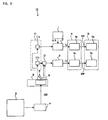
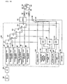
FIG. 8 shows the first configuration example that
realizes the first selection mode. This configuration
example comprises a power source unit 6, which is
provided with power generating means 6a and a secondary
battery 6b that is charged by the power generating
means 6a, time information generating means 2, function
information generating means 3, power-saving operation
state setting means 11 for causing the information
generating means 2 and 3 to perform power-saving.
operation, and preferential operation selecting means 9
for delivering a command for driving any one of the
power-saving operation state setting means 11 and the
function information generating means 3, thereby
selecting the power-saving operation and the functional
operation. The first configuration example further
comprises residual capacity detecting means 14b for
detecting the voltage of the secondary battery 6b,
thereby detecting the residual capacity of the
secondary battery, power generation detecting means 14a
for detecting the quantity of electricity generated by
the power generating means 6a, and preferential
condition means 9a for selecting the preferential
operation in accordance with detection signals from the
residual capacity detecting means 14b and the power
generation detecting means 14a.
The power source unit 6 supplies driving power to
an electronic circuit 20 that include the aforesaid
individual means through terminals Vdd and Vss. A
reverse-current preventing diode 6c is connected
between the power generating means 6a and the secondary
battery 6b, whereby electric discharge from the
secondary battery 6b to the power generating means 6a
is prevented.
In connecting the preferential operation
selecting means 9 to the power-saving operation state
setting means 11 and the function information
generating means 3, a command for driving any one of
the power-saving operation state setting means 11 and
the function information generating means 3 can be
given by providing one of junctions with reversal means.
FIG. 9 shows the second configuration example
that realizes the second selection mode. This
configuration example comprises a power source unit 6,
time information generating means 2, and function
information generating means 3, which are similar to
those of the first configuration example. Power-saving
operation state setting means 11 subjects individual
information generated by the time information
generating means 2 and the function information
generating means to power-saving operation, and these
information are selected by preferential operation
selecting means 90 and delivered to display means 5.
The preferential operation selecting means 90 can be
configured to comprise a selector 90b, which selects
time information and function information applied to a
terminal A and a terminal B and delivers them to the
display means 5, and preferential condition means 90a,
which delivers a selection signal for preferential
operation to a terminal C of the selector 90b in
accordance with detection signals from residual
capacity detecting means 14b and power generation
detecting means 14a.
In the case where the power-saving operation is
given priority in this configuration example, the
power-saving operation state setting means 11 is driven
in response to a command from the preferential
condition means 90a. In the case where the function
information is given priority, the function information
is preferentially delivered to the display means 5 by
delivering a command from the preferential condition
means 90a for selecting the function information to the
terminal C.
In the first and second configuration examples,
the power-saving operation state setting means 11
restricts the generation and/or display on the time
information and/or the function information in
accordance with the detection signal from the residual
capacity detecting means 14b and/or the detection
signal from the power generation detecting means 14a.
Further, power generated by the power generation
detecting means 14a can be detected according to the
voltage, current, and generation time.
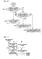
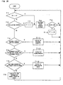
FIG. 10 is a flowchart showing an example of the
procedure of selecting operation according to the first
selection mode, and FIG. 11 is a diagram for
illustrating selecting operation for the power
generating voltage and secondary battery voltage.
Va and VA are individually settled in advance as
set levels for the secondary battery voltage and the
power generating voltage. Va is settled as a level to
determine whether or not to perform function
information display, and VA is settled as a level to
determine whether or not to perform power-saving
operation.
First, the secondary battery voltage is compared
with the level Va. If the secondary battery voltage is
not lower than the level Va (Step S11), the function
information is displayed (Step S12). If the secondary
battery voltage is lower than the level Va (Step S11),
on the other hand, the power generating voltage is
compared with the level VA. If the comparison with the
level Va indicates that the power generating voltage is
not lower than the level VA (Step S13), the time
information is displayed in the normal operation state
(Step S14). If the power generating voltage is lower
than the level VA (Step S13), the time information is
displayed in the power-saving operation state (Step
S15).
In FIG. 11, symbols A and B designate terminals
that are selected by the selector 9b of FIG. 9. The
terminal B is selected when the function information is
displayed, and the terminal A is selected when the time
information is displayed (normal operation state and
power-saving operation state).
The second selection mode will now be described
with reference to FIGS. 12 to 15. In the second
selection mode, the functional operation and the power-saving
operation are selected according to the power
generating voltage level VA.
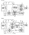
FIGS. 12 and 13 show first and second
configuration examples that realize the second
selection mode, respectively. The configuration
examples shown in FIGS. 12 and 13 can be arranged
substantially in the same manner as the configuration
examples of FIGS. 8 and 9 for the first selection mode
except for the residual capacity detecting means 14b.
Since other configurations are common, a description of
FIGS. 12 and 13 is omitted herein. According to the
second selection mode, the preferential operation
selecting means 9 and 90 perform selecting operation in
accordance with the detection signal from the power
generation detecting means 14a.
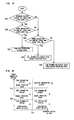
FIG. 14 is a flowchart showing an example of the
procedure of selecting operation according to the
second selection mode, and FIG. 15 is a diagram for
illustrating selecting operation for the power
generating voltage.
VA and VB are individually settled in advance as
set levels for the power generating voltage. Although
VA > VB is given in this embodiment, the relation
between the set levels is not limited to it. Va is a
level to determine whether or not to perform function
information display, and VA is a level to determine
whether or not to perform power-saving operation.
First, the power generating voltage is compared
with the level VA. If the power generating voltage is
not lower than the level VA (Step S21), the function
information is displayed (Step S22). If the power
generating voltage is lower than the level VA (Step
S21), on the other hand, the power generating voltage
is compared with the level VB. If the comparison with
the level VB indicates that the power generating
voltage is not lower than the level VB (Step S23), the
time information is displayed in the normal operation
state (Step S24). If the power generating voltage is
lower than the level VB (Step S23), the time
information is displayed in the power-saving operation
state (Step S25).
In FIG. 15, symbols A and B designate terminals
that are selected by a selector 9b of FIG. 13. The
terminal B is selected when the function information is
displayed, and the terminal A is selected when the time
information is displayed (normal operation state and
power-saving operation state).
The third selection mode will now be described
with reference to FIGS. 16 to 19. In the third
selection mode, the power-saving operation and the
functional operation are selected according to two
power generating voltage levels and the secondary
battery voltage.
FIGS. 16 and 17 show first and second
configuration examples that realize the third selection
mode, respectively. The configuration examples shown in
FIGS. 16 and 17 are arranged substantially in the same
manner as the configuration examples of FIGS. 8 and 9
for the first selection mode. AND circuits 9a1 and 90a1
are used as the preferential condition means 9a and 90a,
respectively, and the logical product of the detection
signals from the residual capacity detecting means 14b
and the power generation detecting means 14a is used as
a selection signal.
Since other configurations are common, a
description of FIGS. 16 and 17 is omitted herein.
According to the third selection mode, therefore, the
preferential operation selecting means 9 and 90 perform
selecting operation in accordance with the logical
product of the detection signals from the residual
capacity detecting means 14b and the power generation
detecting means 14a.
FIG. 18 is a flowchart showing an example of the
procedure of selecting operation according to the third
selection mode, and FIG. 19 is a diagram for
illustrating selecting operation for the power
generating voltage and the secondary battery voltage.
Va is settled in advance as a set level for the
secondary battery voltage, and VA and VB are settled as
set levels for the power generating voltage. Although
VA > VB is given in this embodiment, the relation
between the set levels is not limited to it. Va and VA
are levels to determine whether or not to perform
function information display, and VB is a level to
determine whether or not to perform power-saving
operation.
First, the secondary battery voltage is compared
with the level Va. If the secondary battery voltage is
not lower than the level Va (Step S31), the power
generating voltage is further compared with the level
VA (Step S32). If the comparison with the level VA
indicates that the power generating voltage is not
lower than VA (Step S32), the function information is
displayed (Step S33).
If the secondary battery voltage is lower than
the level Va (Step S31) and if the power generating
voltage is lower than the level VA (Step S32), on the
other hand, the power generating voltage is compared
with the level VB (Step S34). If the comparison with
the level VB indicates that the power generating
voltage is not lower than the level VB (Step S34), the
time information is displayed in the normal operation
state (Step S35). If the power generating voltage is
lower than the level VB (Step S34), the time
information is displayed in the power-saving operation
state (Step S36).
In FIG. 19, symbols A and B designate terminals
that are selected by a selector 90b of FIG. 17. The
terminal B is selected when the function information is
displayed, and the terminal A is selected when the time
information is displayed (normal operation state and
power-saving operation state).
The fourth selection mode will now be described
with reference to FIGS. 20 to 23. In the fourth
selection mode, the power-saving operation and the
functional operation are selected according to two
power generating voltage levels and the secondary
battery voltage.
FIGS. 20 and 21 show first and second
configuration examples that realize the fourth
selection mode, respectively. The configuration
examples shown in FIGS. 20 and 21 are arranged
substantially in the same manner as the configuration
examples of FIGS. 8 and 9 for the first selection mode.
OR circuits 9a2 and 90a2 are used as the preferential
condition means 9a and 90a, respectively, and the
logical sum of the detection signals from the residual
capacity detecting means 14b and the power generation
detecting means 14a is as a selection signal.
Since other configurations are common, a
description of FIGS. 20 and 21 is omitted herein.
According to the fourth selection mode, therefore, the
preferential operation selecting means 9 and 90 perform
selecting operation in accordance with the logical sum
of the detection signals from the residual capacity
detecting means 14b and the power generation detecting
means 14a.
FIG. 22 is a flowchart showing an example of the
procedure of selecting operation according to the
fourth selection mode, and FIG. 23 is a diagram for
illustrating selecting operation for the power
generating voltage and the secondary battery voltage.
Va is settled in advance as a set level for the
secondary battery voltage, and VA and VB are settled as
set levels for the power generating voltage. Although
VA > VB is given in this embodiment, the relation
between the set levels is not limited to it. Va and VA
are levels to determine whether or not to perform
function information display, and VB is a level to
determine whether or not to perform power-saving
operation.
First, the secondary battery voltage is compared
with the level Va, and the power generating voltage is
compared with the level VA. If the secondary battery
voltage is not lower than the level Va or if the power
generating voltage is not lower than the level VA (Step
S41), the function information is displayed (Step S42).
If the secondary battery voltage is lower than
the level Va and if the power generating voltage is
lower than the level VA (Step S41), on the other hand,
the power generating voltage is compared with the level
VB (Step S43). If the comparison with the level VB
indicates that the power generating voltage is not
lower than the level VB (Step S43), the time
information is displayed in the normal operation state
(Step S44). If the power generating voltage is lower
than the level VB (Step S43), the time information is
displayed in the power-saving operation state (Step
S45).
In FIG. 23, symbols A and B designate terminals
that are selected by a selector 90b of FIG. 21. The
terminal B is selected when the function information is
displayed, and the terminal A is selected when the time
information is displayed (normal operation state and
power-saving operation state).
The fifth selection mode will now be described
with reference to FIGS. 24 to 27. In the fifth
selection mode, the functional operation and the power-saving
operation are selected in response to external
operation.
FIGS. 24 and 25 show first and second
configuration examples that realize the fifth selection
mode, respectively. The configuration examples shown in
FIGS. 24 and 25 can be arranged substantially in,the
same manner as the configuration examples of FIGS. 8
and 9 for the first selection mode except for external
operation detecting means 14c. The external operation
detecting means 14c can be composed of an external
operation member, such as switch means, setup memory,
or wire. According to the switch means or any other
external operation member, selection can be made at any
desired point of time after the electronic timepiece is
manufactured. In the case where selection is made in
the process of manufacturing an electronic timepiece,
moreover, such selection can be made by setup in a
memory in an IC circuit or by a hardware configuration
based on wire option. Since other configurations are
common, a description of FIGS. 24 and 25 is omitted
herein. According to the fifth selection mode, the
preferential operation selecting means 9 and 90 perform
selecting operation in accordance with a signal by the
external operation.
FIG. 26 is a flowchart showing an example of the
procedure of selecting operation according to the fifth
selection mode, and FIG. 27 is a diagram for
illustrating the external operation and selecting
operation for the power generating voltage.
A level VA to determine whether or not to perform
power-saving operation is settled in advance for the
power generating voltage.
First, the selection of preference to function
information by external operation means is detected
(Step S51). If the preference to function information
is selected (Step S51), the function information is
displayed (Step S52). If the preference to function
information is not selected (Step S51), on the other
hand, the power generating voltage is compared with the
level VA (Step S52). If the comparison with the level
VA indicates that the power generating voltage is not
lower than the level VA (Step S53), the time
information is displayed in the normal operation state
(Step S54). If the power generating voltage is lower
than the level VA (Step S53), the time information is
displayed in the power-saving operation state (Step
S55).
In FIG. 27, symbols A and B designate terminals
that are selected by a selector 90b of FIG. 25. The
terminal B is selected when the function information is
displayed, and the terminal A is selected when the time
information is displayed (normal operation state and
power-saving operation state).
The selection of the functional operation and the
power-saving operation in response to the external
operation according to the fifth selection mode can be
combined with the first to fourth selection modes. The
priority between the fifth selection mode based on the
external operation and the first to fourth selection
modes can be set by separate selecting means.
As described in connection with the foregoing
configurations, the electronic timepiece of the present
embodiment may be composed of hardware or software. FIG.
28 is a diagram showing a configuration example of the
electronic timepiece of the present embodiment based on
software. In FIG. 28, the individual functions the
electronic circuit 20 in each of the foregoing
configuration examples performs can be composed of a
CPU·IC 40 for analog electronic timepiece control, ROM
42, and RAM 43. The ROM 42 is loaded with a program for
generating time information, a program for generating
function information, a program for performing
preferential operation selection, and a program for
realizing the functions of other electronic timepieces.
Further, the CPU·IC 40 for analog electronic timepiece
control has an oscillator circuit therein, and forms
clock signals by using the output of a crystal
oscillator 41.
The CPU·IC 40 for analog electronic timepiece
control is connected with the power generation
detecting means 14a for detecting the state of power
generation of the power generating means 6a, the
residual capacity detecting means 14b for detecting the
residual capacity by detecting the voltage of the
secondary battery 6b or the like, and an input
operation switch element 44 for inputting various
operations and selection for the electronic timepiece,
and detection signals, control signal and selection
signal are inputted to the CPU·IC 40 for analog
electronic timepiece control. Further, the CPU·IC 40
for analog electronic timepiece control is connected
with a buzzer 45, hour hand 21, minute hand 22 and
second hand 23, and displays the time information and
function information. Besides the hour hand 21, minute
hand 22, and second hand 23, liquid crystal display
means may be used as the display means.
FIG. 29 shows a configuration example of the
electronic timepiece 10 according to the present
embodiment.
This electronic timepiece has a dial plate 24 for
ordinary time information display and a minute hand 30
for chronographic display, as well as the hour and
minute hands 21 and 22 and the second hand 23. In this
example, the second hand 23 serves also as a
chronographic second hand for chronographic display.
Further, this configuration example is provided
with a mode display hand 25, and different functions
can be set depending on the position of the mode
display hand 25. In this configuration example, the
mode display hand 25 can be shifted between two
different positions, a time information display
position (TME) 26 for displaying normal time
information and a chronographic display position (CHR)
27 for executing a chronographic display function, and
can be moved to the position TME 26 or CHR 27 by
operating a stem 33.
Thus, if the mode display hand 25 is set in the
time information display position (TME) 26, according
to the present configuration example, the hour and
minute hands 21 and 22 and the second hand 23
individually indicate the current time. If the mode
display hand 25 is set in the chronographic display
position (CHR) 27, on the other hand, the hour and
minute hands 21 and 22 indicate the hour and minute,
respectively, of the current time, and when a starting
operation is carried out after shift to a chronographic
mode at the set point of time, the chronographic
display function is started, so that the second hand 23
indicates the chronographic second, and along with the
chronographic minute hand 30, indicates the
chronographic time.
If the requirements for the power-saving
operation state are detected when the mode display hand
25 is set in the time information display position
(TME) 26 or the chronographic display position (CHR) 27,
the second hand 23 is moved to a power-saving position
29 (e.g., position for 0 second) automatically or with
the user's depression of a button PB1 or PB2, thereby
indicating that the electronic timepiece 10 is set in
the power-saving operation state.
The power-saving operation state can be canceled
by automatic processing based on a detection signal for
detecting the failure to fulfill the requirements for
the power-saving operation state or manual operation in
which the specific button PB1 or PB2 on the electronic
timepiece is depressed.
The functions of the electronic timepiece include
an alarm function, chronographic display function,
calendar function, sounding function, and altitude
measuring function. In the case where the electronic
timepiece is a rechargeable, generator-type electronic
timepiece having power generating means such as a solar
cell, in particular, moreover, the function information
of the present invention further includes time
adjustment warning function information for warning of
wrong time indication when the electronic timepiece
undercharged and temporarily stopped is restarted by
recharge, charge warning function information or a
warning for prompting charge, and residue warning
function information for indicating the residual
capacity of the secondary battery or accumulator for
use as accumulator means. In the case where the power
generating means is a solar cell, in particular, if the
power-saving state is given priority after the darkened
ambiance of the watch is detected, then the ambiance is
too dark to sight the display and visually recognize
the aforesaid warning information, anyway. It is very
reasonable, therefore, to stop the display means in the
power-saving state.
In the case where the power generating means is
of the self-winding or thermal generator type, moreover,
the darkness of the ambiance of the watch and the
performance of power generation are independent of each
other, and the aforesaid circumstances do not apply to
this case. Naturally, the same effect can be obtained
with use of any other power generating means than a
solar cell only if it is provided with a sensor for
detecting the darkness of the ambiance of the watch.
As described above, the electronic timepiece
according to the first embodiment and the driving
method for the electronic timepiece use the foregoing
technical configurations. In the field of
multifunctional electronic timepieces that can provide
many kinds of additional function information,
therefore, there may be easily realized an electronic
timepiece with high commercial value that is configured
to be able to use the power-saving mode and the
function information operation state mode separately
and a driving method for the electronic timepiece. Thus,
the power-saving mode and the function information
operation state mode can be selected and preferentially
controlled.
An outline of a second embodiment of the present
invention will now be described with reference to FIGS.
30A to 45.
An electronic timepiece according to the present
embodiment comprises means for giving priority to a
power-saving operation state, functional operation
state, or warning operation state. Even if the power-saving
operation state, functional operation state, and
warning operation state for display means are
competitive, any one of the power-saving operation
state, functional operation state and warning operation
state is adopted according to priority.
More specifically, the present embodiment is
configured to give priority to any one of the power-saving
operation state, functional operation state and
warning operation state according to circumstances by
selection by preferential operation selecting means.
FIGS. 30A and 30B are diagrams for illustrating
several means of the electronic timepiece of the
present embodiment and their operations. In FIGS. 30A
and 30B, any one of the power-saving operation state,
functional operation state and warning operation state
is given priority by selecting and operating power-saving
operation means, function information generating
means, or warning information generating means by the
preferential operation selecting means.
The electronic timepiece according to the present
embodiment will now be described with reference to FIGS.
30A and 30B.
In FIG. 30A(a), an electronic timepiece 10
comprises time information generating means A for
generating time information, function information
generating means B for generating function information
on additional functions, such as a chronographic
measuring function, timer function, alarm function,
sounding function, altitude measuring function, time
radio-wave modifying function, computer function, etc.,
warning information generating means F for generating
warning information such as a charge warning, residue
warning, time adjustment warning, etc., display means C
capable of alternatively displaying the time
information, function information, or warning
information, power-saving operation means D for
operation in the power-saving operation state that
entails lower power consumption than a normal operation
state, and preferential operation selecting means E for
giving priority to the function information generating
means B, warning information generating means F, or
power-saving operation means D. The time information
generating means A and the function information
generating means B, which generate the time information
and the function information, which are general
information, constitute general information generating
means G.
In the normal operation state, as shown in FIG.
30A(b), the preferential operation selecting means E
gives priority to neither the function information
generating means B, nor the power-saving operation
means D, nor the warning information generating means F,
and the display means C continually displays the time
information. If a function command for the selective
use of the function information is given, it is
displayed on the display means C.
On the other hand, the display of the time
information, function information, and warning
information is stopped if neither the function command
nor a warning command which is an operation command
directing to the warning information generating means F
is given with a power-saving command given to the
power-saving operation means D by the preferential
operation selecting means E, as shown in FIG. 30A(c).
FIG. 30B(d) shows the case where the warning
command is given in the presence of the power-saving
command for ordering the power-saving operation. A
warning display state is given priority over the power-saving
state under the control of the preferential
operation selecting means E, and the display means C is
brought to the warning display state. In display stop
operation for the time information, moreover, counting
the time information can be continued.
If the function information generating means B is
given priority by a function-first command from the
preferential operation selecting means E, as shown in
FIG. 30B(e), furthermore, the display of the function
information is given priority over the power-saving
operation.
FIG. 30B(f) shows a state in which the warning
command is given as a warning-first command with the
function-first command given from the preferential
operation selecting means E. In this case, the warning
display state is given priority over the function
information display state that gives priority over the
power-saving operation. Thus, the warning display is
more important as display information on the watch than
any other general information including the time
information and the function information, and should be
given the highest priority. As described with reference
to FIG. 30B(d) or 30B(f), therefore, the display state
for the warning information is given priority over the
power-saving operation state and the function
information display state. Thus, the electronic
timepiece that displays the time information, function
information, and warning information and has the power-saving
operation state is made reasonable and easy to
handle.
The following is a description of a specific
configuration of the second embodiment.
FIG. 31 is a block diagram showing the principal
part of an electronic timepiece of a second example. In
FIG. 31, a power source is connected to an electronic
timepiece 55. In this example, the power source is
composed of power generating means 51, such as a solar
cell, self-winding generator system, windup generator
system, thermal generator means, or spring-type
generator system, accumulator means 53, such as a high-capacity
condenser or secondary battery, Zener diode 54
for use as overcharge preventing means, and diode 52
for preventing reverse-current charge. When light such
as the sunlight is incident upon the solar cell 51,
electricity is generated, the accumulator means 53 is
charged through the diode 52, the charged voltage of
the accumulator means 53 is applied to the electronic
timepiece 55, and electric power is applied to the
electronic timepiece 55.
Numeral 56 denotes a reference signal generator
circuit, which outputs a group of reference signals P6
(including a plurality of pulses with different periods
divided from a time base source 161). Numeral 60
denotes an hour-minute hand movement signal generator
circuit, which outputs a twenty-second step pulse
signal P10 that causes hour and minute hands to rotate
so that the minute hand makes two revolutions (and the
hour hand makes a 1/6 revolution) for each twenty
seconds, in the normal operation state, and causes a
second motor drive circuit 68 to drive a second pulse
motor 71, thereby driving the minute and hour hands of
a display unit 70. Numeral 61 denotes a normal signal
generator circuit of the watch for use as means for
generating general information, and outputs a one-second-step
pulse P11 (accurate time information
signal) as a normal second-hand movement signal in the
normal operation state. Although the time information
is given as an example of the general information in
the present embodiment, the general information also
include function information, such as chronographic
information, timer information, alarm function
information, etc., which are added to the watch. The
output of the normal signal generator circuit 61 is
applied to an A-input terminal of a first selection
circuit 64 for use as a selector. (A selector described
herein is a control circuit designed so that the input
applied to its A-input terminal is selected and
delivered to its Q-terminal when an input to its C-terminal
is at "L" level and that the input to its B-input
terminal is selected and delivered to the Q-terminal
when the input to the C-terminal is at "H"
level, and the following selectors are control circuits
having the same functions.)
Numeral 62 denotes a first modulation signal
generator circuit, which generates a charge warning
signal for urging the user to establish a state where
the watch is charged (e.g., light is applied in the
case of the watch that has the solar cell as charging
means or the watch is carried around and vibrated in
the case of the watch of the self-winding generator
type). This signal is a two-second-step pulse P12 for
two-second-step drive (e.g., pulse that generates a
pair of driving pulses of a 40-ms duration at intervals
of two seconds), and is originated and outputted in
accordance with a specific reference signal P6. This
output is applied to the B-input terminal of the first
selection circuit 64. An output signal P14 from the Q-terminal
of the first selection circuit 64 is either
the one-second-step pulse P11 or the two-second-step
pulse P12, which is applied to the A-input terminal of
a second selection circuit 65 for use as a selector.
In a first example of the present embodiment, the
hour-minute hand movement signal generator circuit 60
and the normal signal generator circuit 61, which
output accurate time information signals, constitute
general information generating means.
Numeral 63 denotes a second modulation signal
generator circuit, which generates a run-down state
warning signal P13 that informs the user that the watch
is run-down. This run-down state warning signal P13 is
an irregular two-second-step pulse P13 that is
modulated for an irregular speed different from that of
the two-second-step pulse P12 based on the output of
the first modulation signal output circuit (e.g., pulse
that alternately generates driving pulses of a 40-ms
duration and driving pulses of a 250-ms duration at
intervals of two seconds), and is originated and
outputted in accordance with the specific reference
signal P6. This output is applied to the B-input
terminal of the second selection circuit 65, and the Q-output
signal P14 of the first selection circuit 64 is
applied to the A-input terminal. A Q-output signal P15
of the second selection circuit 65 is applied to the A-input
terminal of a third selection circuit 66 for use
as a selector. The first modulation signal generator
circuit 62 and the second modulation signal generator
circuit 63 constitute warning information generating
means in this example.
Further, an output signal P25 from power-saving
state control means 75 (mentioned later) is applied to
the B-input terminal of the third selection circuit 66,
and an output signal P16 from the Q-terminal of the
third selection circuit 66 is applied to an I-terminal
of a first motor drive circuit 67 for driving the
second hand of the watch.
The first motor drive circuit 67 converts the
driving signal applied to its I-terminal into a bipolar
driving pulse P17 that suits a double-pole pulse motor,
outputs it through its Q-terminal, and drives a first
pulse motor 69. Besides, it is provided with a reset
input terminal R for fixing an operation that
corresponds to a time adjustment state when an
external-operation switch, e.g., the stem, of the watch
is pulled. The first pulse motor 69 is a conventional
pulse motor that has a permanent magnet rotor that is
magnetized for two poles. Numeral 70 denotes a display
device that displays the time and the like, and the
second hand of the display device 70 is driven by the
first pulse motor 69.
Numeral 57 denotes a voltage detection circuit
for detecting an undercharged state. If the supply
voltage of the accumulator means 53 is lowered so that
the normal working state of the watch changes into a
state that requires charge, an output signal P7 is
delivered at "L" level in a state where the supply
voltage is higher than a reference voltage V1 that
urges the user to establish the state for the charge of
the watch. This output is a C-terminal input of the
first selection circuit 64, and the first selection
circuit 64 selects the A-input terminal and outputs the
one-second-step pulse P11 for the normal state through
its Q-terminal. If the voltage drops and becomes lower
than the reference voltage V1, however, the detection
signal P7 turns to "H" level. Thereupon, the two-second-step
pulse P12 of the B-input is selectively
outputted, in place of the one-second-step pulse P11,
from the Q-terminal of the first selection circuit 64.
A reference signal stop storage circuit 58 uses a
512-Hz output signal P62 of a first frequency divider
circuit 162 of the reference signal generator circuit
56 and a 1/2-Hz output signal P63 of a second frequency
divider circuit 163 to monitor oscillating operation of
the time base 161 of the reference signal generator
circuit 6. If the oscillation stops, a stop detection
signal P81 is outputted from a K-terminal, and the
second frequency divider circuit 163 is reset. The
reference signal stop storage circuit 8 is stored with
the stoppage of the oscillation. If the supply voltage
is recovered thereafter to restore the oscillation, a
reference signal stop storage signal P8 of "H" level is
then outputted. When this signal P8 is applied to the
C-terminal of the second selection circuit 65 through
an OR gate 126, the irregular two-second-step pulse P13,
which is a run-down state warning signal, is selected
as the signal P15. This reference signal stop storage
signal P8 is reset at "L" level when a reset signal is
applied to an R-terminal of the reference signal stop
storage circuit 58. Since the details of the reference
signal stop storage circuit 8 are generally known, a
detailed description of them is omitted (see Japanese
Patent Application Laid-Open No. 62-194484 and the like
for details).
A pulse motor stop storage circuit 59 can observe
time-based change of induced voltage that is generated
in a coil by residual vibration in a rotor and
determines whether or not the rotor is rotated normally
or is not rotated, immediately after the twenty-second-step
pulse signal P10 is given to the second motor
drive circuit 68 that monitors the detection of normal
operation of the second pulse motor 71 by transmitting
to or receiving signals from the second motor drive
circuit 68. The pulse motor stop storage circuit 59
receives the twenty-second-step pulse signal P10 from
the hour-minute hand movement signal generator circuit
60 at its F-terminal, originates some strobe signals
P91 for fetching induced voltage with given timing
based on the reference signal P6 applied to its E-terminal,
and delivers them through its G-terminal to
an N-terminal of the second motor drive circuit 68. The
second motor drive circuit 68 outputs a series of
induced voltage signals for induced voltage values for
individual instants, and returns them to a Y-terminal
of the pulse motor stop storage circuit 59. If it is
determined in accordance with the induced voltage
signals that the rotor is not rotated, the
determination is stored. When the rotation of the
second pulse motor 21 is stopped, a pulse motor stop
storage signal P9 of "H" level is delivered to an
output terminal Q. The signal P9 is applied to one
terminal of the OR gate 126. As mentioned before, the
reference signal stop storage signal P8 of the
reference signal stop storage circuit 58 is applied to
the other input terminal of the OR gate 126. The output
of the OR gate 126 is applied to the C-terminal of the
second selection circuit 65 and an OR gate 128. This
pulse motor stop storage circuit 59 is also a
conventional one, and a detailed description of its
configuration is omitted (see Japanese Patent
Application Laid-Open No. 62-194484 and the like for
details).
Numeral 74 denotes a manual switch circuit, which
changes the state by an external-operation switch or by
pushing or pulling a stem. When the stem is pulled, for
example, a reset signal P24 of "H" level is outputted.
The reset signal P24 is applied to the reference signal
stop storage circuit 58, the pulse motor stop storage
circuit 59, and the respective reset terminals R of the
first and second motor drive circuits 67 and 68, and
moreover, to the power-saving state control means 75.
In response to the reset signal P24, these circuits are
restored their respective initial logical states, and
the memories of the reference signals and the stoppage
of the motor are erased. Manual hand alignment or the
like is carried out on the display with the supply
voltage of the accumulator means 53 in its normal state,
and the stem is pushed in thereafter. Thereupon, the
reset circuits are released together from restriction,
and the watch operation starts from its initial state.
Non-power-generating state detecting means 73,
which detects the power generating state of the power
generating means 51, delivers an output signal P23 of
"H" level when a non-power-generating state lasts for a
preset time.
FIG. 32 is a detailed block diagram of the power-saving
state control means 75. The reference signal P6
from the reference signal generator circuit 56 is
applied to a 64-Hz fast-forward hand movement signal
originating circuit 254. The output signal P11 of the
normal-state signal generator circuit 61 is applied to
a current-second sexagesimal counter 250. The output
signal P16 from the Q-terminal of the third selection
circuit 66 is applied to a second-hand position
sexagesimal counter 251. Further, a signal P64 of 64 Hz
from the second frequency divider circuit 162 of the
reference signal generator circuit 6 is applied to the
64-Hz fast-forward hand movement signal originating
circuit 254, whereupon a fast-forward pulse P254 is
originated by also using the reference signal P6.
Furthermore, the reset signal P24 from the manual
switch circuit 74 is applied to the respective reset
terminals of the current-second sexagesimal counter 250
and the second-hand position sexagesimal counter 251,
and resets these counters. The output P23 of the non-power-generating
state detecting means is applied to
one terminal of an AND gate 255 and to one terminal of
an AND gate 256 through an inverter I253. Count values
in the current-second sexagesimal counter 250 and the
second-hand position sexagesimal counter 251 are
compared with each other in a coincidence detection
circuit 252. If they are equal, an output signal of "H"
level is delivered and applied to the other terminal of
the AND gate 256 through an inverter I251. Further, a
zero detection circuit 253 is provided that receives
the output signal of the second-hand position
sexagesimal counter 251 as its input and detects a zero
count value of the second-hand position sexagesimal
counter 251. If the zero detection circuit 253 detects
zero, an output signal of "H" level is delivered and
applied to the other terminal of the AND gate 255
through an inverter I252. The respective outputs of
these two AND gates are applied to an input terminal of
an AND gate 258 through an OR gate 257, while the fast-forward
pulse P254 from the 64-Hz fast-forward hand
movement signal originating circuit 254 is applied to
the other terminal. The output of the AND gate 258 is
applied as the output signal P25 of the power-saving
state control means to the B-input terminal of the
third selection circuit 66. An output signal P256 of
the AND gate 256 is delivered from the power-saving
state control means 75 to an OR gate 129. The output
signal P23 of the non-power-generating state detecting
means 73 is applied to the other terminal of the OR
gate 129. The output of the OR gate 129 is applied to
an AND gate 127, and the output of the NOR gate 128 is
applied to the other terminal of the AND gate 127.
Further, the output signal P7 of the voltage detection
circuit 57 and the output signal of the OR gate 126 are
applied to the NOR gate 128. Furthermore, the output of
the AND gate 127 is applied to the C-terminal of the
third selection circuit.
The following is a description of the operation
of this example. First, the voltage of the accumulator
means 53 is not lower than the reference voltage, and
the voltage detection signal P7 of "L" level is
delivered from the voltage detection circuit 7, and the
power generating means 1 is generating power. The
output signal P23 of the non-power-generating state
detecting means 73 indicates that electricity is being
generated when it is at "L" level. In this normal state,
the hour-minute hand movement signal generator circuit
60 outputs the twenty-second-step pulse signal P10 that
drives the minute and hour hands in accordance with the
reference signal P6 from the reference signal generator
circuit 56, and the second motor drive circuit 68
drives the second pulse motor 71, thereby driving the
hour and minute hands of the display device 70 to
display the current hour and minute. Since the output
signal P7 of the voltage detection circuit 7 is at "L"
level, on the other hand, an "L" level signal is
applied to the C-terminal of the first selection
circuit 64, whereupon the A-input terminal is selected.
Since both the reference signal stop storage signal P8,
which is an output signal of the reference signal stop
storage circuit 58, and the pulse motor stop storage
signal P9 from the pulse motor stop storage circuit 59
are at "L" level in the normal state, the output signal
of the OR gate 126 is at "L" level, and an "L" level
signal is applied to the C-terminal of the second
selection circuit 65, whereupon the A-input terminal is
selected.
When the power generating means 51 is generating
power, moreover, the output signal P23 of the non-power-generating
state detecting means 73 is at "L"
level, and the output signal P256 from the AND gate 256
of the power-saving state control means 75 is also at
"L" level, so that the output signal of the OR gate 129
is also at "L" level. In consequence, the output of the
AND gate 127 turns to "L" level, so that an "L" level
signal is applied to the C-terminal of the third
selection circuit 66, whereupon the A-input terminal is
selected. Accordingly, the one-second-step pulse P11,
which is an output signal of the normal-state signal
generator circuit 61, is applied as the signal P16 to
the I-terminal of the first motor drive circuit 67
through the respective A-input terminals and Q-terminals
of the first, second, and third selection
circuits 64, 65 and 66. The first pulse motor 69 is
driven by the output signal P17 of the first motor
drive circuit 67, and the second hand of the display
device 70 is driven to tick the seconds as a normal
one-second movement hand. Thus, the display device 70
performs the normal display of the hour, minute, second
for the time.
If the non-power-generating state detecting means
73 detects that electricity is not generated for the
preset time, and if the output signal P23 of the non-power-generating
state detecting means 73 turns to "H"
level, in this normal state, the respective outputs of
the OR gate 129 and the AND gate 127 turn to "H" level.
Since the "L" level voltage detection signal P7 from
the voltage detection circuit 57 and the output signal
of the OR gate 126 at "L" level are the inputs of the
NOR gate 128, moreover, the output signal of the NOR
gate 128 is at "H" level. If the output signal P23 of
the non-power-generating state detecting means 73 turns
to "H" level, as mentioned before, the output of the
AND gate 127 delivered through the OR gate 129 turns to
"H" level, so that the output signal of the AND gate
127 also turns to "H" level. In consequence, an "H"
level is applied to the C-terminal of the third
selecting means, so that the third selecting means 66
selects the B-terminal side. Since the voltage
detection signal P7 and the output signal of the OR
gate 126 are at "L" level, the first and second
selecting means 64 and 65 select the A-input terminal
side.
In the power-saving state control means 75 (see
the operation timing chart of FIG. 33 for the power-saving
state control means 75), on the other hand, the
count value of the current-second sexagesimal counter
250 and the count value of the second-hand position
sexagesimal counter 251 are equal in the normal state
for power generation. Therefore, an "H" level signal is
delivered from the coincidence detection circuit 252,
and this signal is inverted and turned into an "L"
level signal by the inverter I251 and applied to the
AND gate 256. In consequence, the output signal P256 of
the AND gate 256 is at "L" level. Since the "L" level
signal P23 is delivered from the non-power-generating
state detecting means 73 while electricity is being
generated, moreover, the output of the AND gate 255 is
at "L" level. In consequence, the output of the OR gate
257 is also at "L" level, and the AND gate 258 is
closed, so that no output signal is delivered from the
AND gate 258. Thus, no output is delivered from the
power-saving state control means 75.
If the non-power-generating state detecting means
73 detects that the power generation is stopped for the
preset time and outputs the "H" level signal P23,
therefore, the AND gate 255 outputs an "H" level signal
unless the count value of the second-hand position
sexagesimal counter 251 is "0".
The reason is that if the zero detection circuit
253 detects that the count value of the second-hand
position sexagesimal counter 251 is not "0", an "L"
level signal is delivered from the zero detection
circuit 253, and inverted and turned to "H" level by
the inverter I252 and applied to the AND gate 255.
Therefore, both of the two inputs of the AND gate 255
are at "H" level, so that an "H" level output signal is
delivered from the AND gate 255.
Since this "H" level signal is applied to the AND
gate 258 through the OR gate 257, the AND gate 258
opens, whereupon the fast-forward pulse p254 originated
in the 64-Hz fast-forward hand movement signal
originating circuit 254 is outputted as the output
signal P25 of the power-saving state control means 75.
This signal P25 is applied to the B-terminal of the
third selection circuit 66. In the state where power
generation is stopped, as mentioned before, the B-terminal
of the third selection circuit 66 is selected,
so that the fast-forward pulse P254 of the signal P25
is delivered as the signal P16 from the Q-terminal of
the third selection circuit 66 and applied to the first
motor drive circuit 67, whereupon the second hand is
fast-forwarded.
Since the signal P16 from the Q-terminal of the
third selection circuit 66 is applied to the second-hand
position sexagesimal counter 251, moreover, the
second-hand position sexagesimal counter 251 is also
fast-forwarded at 64 Hz as it counts. If the zero
detection circuit 253 detects that the count value of
the counter 251 is "0", an "H" level signal is
delivered from the zero detection circuit 253 and
inverted by the inverter I252, and the input of the AND
gate 255 turns to "L" level. Accordingly, the output of
the AND gate 255 also turns to "L" level, so that the
AND gate 258 is closed, whereupon the fast-forward
pulse p254 ceases to be outputted as the output signal
P25. In consequence, the second hand stops at a
position "0" (upright position). Although the position
"0" is used in this example, the second hand may be
stopped in any desired position. This is because it is
necessary only that power be saved by stopping the
second hand. In many cases, however, the second hand is
stopped at the position "0", since the stoppage of the
second hand at the position "0" is accustomed to serve
also for power-saving mode display. When power
generation is not restarted with the second hand
stopped at the position "0", the output signal P23 of
the non-power-generating state detecting means 73 is at
"H" level, and this signal is inverted by the inverter
I253 so that an "L" level signal is inputted.
Accordingly, the output signal P256 of the AND gate 256
is at "L" level. Since an "H" level signal is delivered
from the zero detection circuit 253, moreover, it is
inverted by the inverter I252 and applied to the AND
gate 255, so that its output signal is "L", therefore,
the input of the AND gate 258 from the OR gate 257 is
at "L" level, so that the gate is closed. In this state,
the output signal P25 of the power-saving state control
means 75 is not outputted at all. Thus, the second hand
is stopped at the position "0" and never moves unless
power generation is restarted. Since the second hand is
not driven, energy consumption can be saved to maintain
the power-saving state.
When the movement of the second hand is stopped
to maintain the power-saving state in this manner, the
current-second sexagesimal counter 250 counts the one-second-step
pulse P11. However, the second position
sexagesimal counter, receiving no input, is set at zero.
Every time the count value of the current-second
sexagesimal counter 250 becomes "0", an "H" level
signal is delivered from the coincidence detection
circuit 252 for the counting period, while an "L" level
signal is outputted in any other sections. Thus, an "L"
level signal is outputted normally. The signal applied
to the AND gate 256 via the inverter I251 is normally
an "H" level signal in any other sections than the
section in which the count value of the current-second
sexagesimal counter 250 is "0".
If power generation is restarted so that the
output signal P23 of the non-power-generating state
detecting means 73 turns to "L" level, an "H" level
signal inverted by the inverter 1253 is applied to the
AND gate 256. Therefore, the "H" level signal P256 is
delivered from the AND gate 256 in any other sections
than the section in which the count value of the
counter 250 is "0". In response to this signal, the AND
gate 258 is opened through the OR gate 257, and the
fast-forward signal P254 from the 64-Hz fast-forward
hand movement signal originating circuit 254 is
outputted as the signal P25. Since the signal P25 is
applied to the second-hand position sexagesimal counter
251, the counter 251 is fast-forwarded at 64 Hz as it
counts. If the resulting count value is equal to the
count value of the current-second sexagesimal counter
250, an "H" level signal is delivered from the
coincidence detection circuit 252, and an "L" level
signal is applied to the AND gate 256 via the inverter
I251, so that the output P256 of the AND gate 256 turns
to "L" level. Thereupon, the AND gate 258 is closed,
and the signal P25 ceases to be outputted. Thus, the
fast-forward signal P254 is delivered as the signal P25
from the power-saving state control means 75 during the
time interval that elapses from the instant that power
generation is restarted until the second hand is moved
to the position indicated by the count value of the
current-second sexagesimal counter 250.
Even if the output signal P23 of the non-power-generating
state detecting means 73 turns to "L" level
as power generation is restarted, on the other hand,
the output of the AND gate 127 is kept at "H" level by
the "H" level output signal P256 of the AND gate 256
that is applied to the OR gate 129, and is applied to
the C-terminal of the third selection circuit. If the
output signal P23 of the non-power-generating state
detecting means 73 turns to "L" level, therefore, the
output of the C-terminal is kept at "H" level. Thus,
the third selection circuit 66 selects the B-terminal
side until the signal P256 turns to "L" level, that is,
until the second hand is fast-forwarded at 64 Hz to the
position indicated by the count value of the current-second
sexagesimal counter 250, and delivers the fast-forward
signal P254 through its Q-terminal. Thereupon,
the first pulse motor 69 is driven by the first motor
drive circuit 67 to fast-forward the second hand. When
the second hand moves to the position indicated by the
count value of the current-second sexagesimal counter
250, the output signal P256 of the AND gate 256 turns
to "L" level, so that the input of the C-terminal turns
to "L" level. Thereupon, the third selection circuit 66
selects the A-terminal and delivers through its Q-terminal
the one-second-step pulse P11, which is an
output signal of the normal signal generator circuit 61,
which is delivered through the respective A-input
terminals and Q-terminals of the first and second
selection circuits 64 and 65, thereby restoring the
second hand to the normal state of movement.
In the process of operation described above, the
non-power-generating state is detected when the watch
is performing the normal operation with the voltage of
the accumulator means 53 not lower than the given
voltage, and the power-saving state is entered. As
power generation is restarted, the power-saving state
is canceled, and the normal watch display is restored.
The following is a description of charge warning
information display operation to be performed when the
voltage of the accumulator means 53 is lower than the
given voltage.
If the voltage of the accumulator means 53 falls
below the given voltage, the output signal P7 of the
voltage detection circuit 7 turns to "H" level.
Thereupon, the input of the C-terminal of the first
selection circuit 64 turns to "H" level, so that the
first selection circuit 64 selects the B-terminal and
delivers the two-second-step pulse signal P12 from the
first modulation signal generator circuit 62 through
its Q-terminal. The inputs applied to the respective C-terminals
of the second and third selection circuits 65
and 66 are at "L" level, and the A-input terminal is
selected. Accordingly, the two-second-step pulse signal
P12 from the first modulation signal generator circuit
62 is applied to the first motor drive circuit 67, and
the first pulse motor 69 is driven by the two-second-step
pulse P12 to move the second hand for two seconds,
thereby giving a warning of charge. Thus, the two-second
movement operation of the second hand serves as
a warning to prompt charge to cope with the lowered
voltage of the accumulator means 53.
Even if the "H" level signal P23, which indicates
a non-power-generating state as power generation has
not been carried out for a predetermined time, is
delivered from the non-power-generating state detecting
means 73 while the charge warning operation is being
carried out, the output of the AND gate 127 is kept at
"L" level without any change (because the "H" level
output signal P7 of the voltage detection circuit 57 is
applied to the NOR gate 128, so that the respective
outputs of the NOR gate 128 and the AND gate 127 are at
"L" level), and the third selection circuit 66 selects
the A-terminal and outputs the two-second-step pulse
P12, which is an output signal of the first modulation
signal generator circuit 62, through its Q-terminal,
thereby continuing the warning for prompting charge.
If the voltage detection circuit 57 detects a
voltage not higher than the reference voltage such that
its output signal P7 is at "H" level in a state where
the "H" level signal P23, which indicates non-power-generating
state, is delivered from the non-power-generating
state detecting means 73 in the power-saving
state, where the aforesaid second hand is stopped at
the position "0", in contrast with this, the output of
the NOR gate 128 turns to "L" level in response to the
"H" level signal of the output signal P7, and the
output of the AND gate 127 also turns to "L" level.
Since the C-terminal of the third selection circuit 66
is turned to "L" level, therefore, the A-terminal is
selected. Thus, the two-second-step pulse P12 or the
output signal of the first modulation signal generator
circuit 62 is applied to the first motor drive circuit
67 through the B-terminal and Q-terminal of the first
selection circuit 64, the A-terminal and Q-terminal of
the second selection circuit 65, and the A-terminal and
Q-terminal of the third selection circuit, whereupon
the operation of the second hand is switched over to
two-second movement where the second hand is driven in
accordance with the two-second-step pulse P12, thereby
giving the warning to prompt charge.
Once the warning state to prompt charge is
established in this manner, the charge warning display
lasts even in the power-saving state. Even if it is
detected that power has not been generated for the
preset time in the charge warning display state,
moreover, the charge warning display state is
maintained without entering the power-saving state.
Thus, warning is displayed with priority over the
power-saving state.
The following is a description of the state
priority relation between the power-saving state and a
run-down state warning display state, warning
information for a state where the watch must be
adjusted to accurate time when the watch is restarted
by recharge after the second pulse motor 71 or the
reference signal generator circuit 56 is stopped.
If the voltage of the accumulator means 53 lowers
so that the second pulse motor 71 is stopped, the pulse
motor stop storage means 59 detects the stoppage of
this pulse motor, whereupon it delivers the "H" level
signal P9 from Q terminal. Even after the voltage of
the accumulator means 3 is recovered so that the drive
of the pulse motor is started, this signal P9 is kept
at "H" level until the stem is pulled so that the reset
signal P24 from the manual switch circuit 74 is
outputted and reset. Further, the reference signal stop
storage circuit 58 stores the fact that the operation
of the reference signal generator circuit 56 is stopped.
If the operation of the reference signal generator
circuit 56, e.g., an oscillator of the time base source
161, is started again as the accumulator means 53 is
recharged, the reference signal stop storage circuit 58
delivers the "H" level signal P8 through its Q-terminal,
and is kept at "H" level until the stem is pulled so
that the reset signal P24 from the manual switch
circuit 74 is reset.
In consequence, after the second pulse motor 71
is stopped or the operation of reference signal
generator circuit 56 is stopped (the pulse motor is
also stopped in this operation stop state), the
accumulator means 53 is recharged so that its voltage
is recovered, and the operations of the reference
signal generator circuit 56 and the pulse motor are
recovered so that the watch starts operation. If the
time display is wrong in a state where time adjustment
has not been performed by pulling the stem, the "H"
level signal P8 or P9 is delivered from the Q-terminal
of the reference signal stop storage circuit 58 or the
Q-terminal of the pulse motor stop storage circuit 59,
and an "H" level signal is applied to the C-terminal of
the second selection circuit 65 through the OR gate 126.
Thereupon, the second selection circuit selects the B-terminal
and delivers the modulated two-second-step
pulse P13 or the output of the second modulation signal
generator circuit 63 through its Q-terminal. Since the
output of the OR gate 126 is at "H" level, moreover,
the output of the NOR gate 128, which receives the
output of the OR gate 126 as its input, turns to "L"
level. Thereupon, the output of the AND gate 127 turns
to "L" level, the C-terminal of the third selection
circuit 66 is adjusted to "L" level, and the A-terminal
is selected. In consequence, the modulated two-second-step
pulse P13, which is an output of the second
modulation signal generator circuit 63, is applied to
the first motor drive circuit 67 through the B-terminal
and Q-terminal of the second selection circuit and the
A-terminal and Q-terminal of the third selection
circuit 66.
While the second hand is being driven by the
modulated two-second-step pulse P13, the time is wrong
with a delay corresponding to the duration of the
stoppage of the pulse motor or the reference signal.
Accordingly, run-down state warning information, which
is warning information that notifies the user of the
necessity of time adjustment, is indicated by irregular
two-second movement of the second hand. In the case
where this run-down state warning information is
displayed, the output of the OR gate 126 is at "H"
level, the output of the NOR gate 128 is at "L" level,
the output of the AND gate 127 is at "L" level, and the
input of the C-terminal of the third selection circuit
66 is at "L" level. Accordingly, the A-terminal is
selected, and the B-terminal is not selected, so that
the mode cannot be switched over to the power-saving
state. This is based on the power-saving state (i.e.,
state in which the input of the C-terminal of the third
selection circuit 66 is at "H" level). In this state,
the respective output signals P9 and P8 of the pulse
motor stop storage circuit 59 and the reference signal
stop storage circuit 8 turn to "H" level as the pulse
motor or the operation of the reference signal
generator circuit 56 is stopped, for example. Even if
electricity is not generated for the preset time and if
the "H" level signal 73 indicative of the non-power-generating
state is delivered from the non-power-generating
state detecting means 73, in this case, the
"L" level signal is applied to the C-terminal of the
third selection circuit 66, as mentioned before, so
that the A-terminal is selected. Thus, the modulated
two-second-step pulse P13 is delivered from the second
modulation signal generator circuit, whereupon the run-down
state warning information, which indicates the
wrongness of the displayed time of the watch and
notifies the user of the necessity of time adjustment
for the watch, is displayed preferentially. If the
respective output signals P9 and P8 of the pulse motor
stop storage circuit 59 and the reference signal stop
storage circuit 8 turn to "H" level in the power-saving
state where aforesaid second hand has been stopped at
the position "0", in contrast with this, the watch is
switched from the power-saving state over to the run-down
state warning information display state under the
same control for the case of the aforesaid warning
information display state (two-second movement) that
prompts charge. Thus, the warning information display
(run-down state warning information and warning
information that prompts charge) is given priority over
the power-saving state.
FIG. 34 is a block diagram of the second example
of the present embodiment. In this second example, the
hand movement of the watch is controlled by a processor,
and warning display and power-saving display are also
controlled by this processor.
In FIG. 34, numeral 100 denotes an analog
electronic timepiece control device that has a CPU
(processor). This analog electronic timepiece control
device 100 is bus-connected with a ROM 101 loaded with
a system program for controlling the electronic
timepiece and a RAM 102 that is used for temporary
storage of data, and moreover, with voltage detecting
means 104 for a secondary battery 103 for use as charge
means to be charged by power generating means 105 such
as a photovoltaic generator or self-winding generator
system, such as the one described in connection with
the first example, and power generation detecting means
106 for detecting whether or not the power generating
means 105 is in a power generating state. The analog
electronic timepiece control device 100 having the CPU
is connected to a driving pulse motor for driving the
minute and hour hands of an hour-minute display device
107 and a pulse motor for driving the second hand of a
second display device 108. The hour-minute display
device 107 and the second display device 108 are
drivingly controlled by drivingly controlling these
pulse motors. Whether or not the pulse motor for
driving the hour-minute display device 107 is being
driven is detected in the same manner as in the first
example, and the result is fed back to the analog
electronic timepiece control device 100 (not shown).
FIG. 35 is a flowchart showing a display
switching process for a normal time display state,
warning display state, power-saving state display state,
etc. that the processor (CPU) of the analog electronic
timepiece control device 100 of this second example
executes.
The processor (CPU) of the analog electronic
timepiece control device 100 determines whether or not
a flag (hereinafter referred to as time adjustment
requiring flag) F1 is set at "1" (Step S1). The time
adjustment requiring flag F1 is stored for a state
where an oscillator in the analog electronic timepiece
control device 100 for generating a reference signal is
stopped, or that the drive of the pulse motor for
driving the hour and minute hands is stopped, and then
no signal (signal indicative of the pullout of the
stem) is delivered from an input operation switch 109
for time adjustment, and the movement of the hour and
minute hands is suspended so that time adjustment has
not been carried out. If the flag 1 is not set at "1",
the processor determines whether or not the oscillator
for generating the reference signal is stopped or the
drive of the pulse motor for driving the hour and
minute hands is stopped (Step S2). If the oscillator is
operating and the pulse motor is driven, the processor
determines whether or not the voltage of the secondary
battery 103 detected by the voltage detecting means 104
is not higher than a reference value (Step S3). If the
reference value is exceeded, the processor determines
by the power generation detecting means 106 whether or
not the non-power-generating state is maintained for
the preset time or longer by the power generating means
105 (step S4). If the power generation is maintained,
the processor determines whether or not a flag F2 (flag
for storing the power-saving state as mentioned later)
is set at "1" (Step S5). If the flag F2 is not set so,
the normal display operation process for the hour,
minute, and second is carried out (Step S8), whereupon
the program returns to Step S1. If power generation is
continued so that the voltage of the secondary battery
is higher than the reference value, thereafter, the
processes of Steps S1 to S5 and S8 are executed
repeatedly, and the watch display in the normal state
is performed. In this second example, the process of
Step S8 constitutes general information generating
means.
If power generation is stopped for the preset
time or longer, on the other hand, the stoppage is
detected in Step S4, and the processor determines
whether or not the flag F2 for storing the power-saving
state is "1" (Step S14). If the flag F2 is not "1", the
display mode is switched over to power-saving state
display (Step S15). Thus, the pulse motor for the
second display device 108 is driven in a fast-forward
mode such that the second hand is situated in the
position "0" (position for twelve o'clock) without
changing the display of the hour and minute (with the
drive of the pulse motor for the hour-minute display
device 107 kept in the normal state), and the second
hand is stopped at the position "0" to switch the mode
over to the power-saving state. Then, the power-saving
state storage flag F2 is set at "1" (Step S16),
whereupon the program returns to Step S1. Thereafter,
the program advances to Steps S1 to S4. If the non-power-generating
state is continued, the program
advances from Step S4 to Step S14, whereupon the
processor determines whether or not the flag F2 is "1".
If the flag F2 is set at "1" in the aforesaid manner,
the program advances to Step S17, whereupon the power-saving
state is maintained. Thus, the pulse motor of
the hour-minute display device 107 is driven so that
the hour and minute hands continue time display.
However, the second hand is kept stopped in the
position "0", thereby indicating the power-saving state.
Thereafter, the processes of Steps S1 to S4, S14 and
S17 are repeatedly executed to maintain the power-saving
state as long as the non-power-generating state
lasts.
If power generation is restarted in a state where
the power-saving state is maintained in this manner,
the restart is detected in Step S4, and the program
advances from Step S4 to Step S5, whereupon the
processor determines whether or not the power-saving
state storage flag F2 is "1". Since the flag F2 is set
at "1" in this case, the pulse motor for second display
is driven in a fast-forward mode to switch the display
mode over to normal-state display such that the second
hand is fast-forwarded to the current second position,
whereupon the flag F2 is reset at "0" (Steps S6 and S7).
Thereafter, the normal operation state is maintained
(Step S8).
If the voltage detecting means detects in Step S3
that the voltage of the secondary battery is not higher
than the reference value, on the other hand, a first
modulated warning display state is entered (Step S13)
without regard to the present state, whether the normal
operation state or the power-saving state. More
specifically, the pulse motor for the second display
device is driven for two pulses every two seconds,
thereby causing the second hand to perform two-second-step
operation, and charge warning display is made to
notify the user that the voltage of the secondary
battery 103 is lowered and requires charge. Thus, the
warning of charge is displayed with priority over the
power-saving state.
If the stoppage of the oscillator or the stoppage
of the drive of the pulse motor is detected in Step S2,
moreover, the time adjustment requiring flag F1 is set
at "1" (Step S9), and the display mode is switched over
to a second modulated warning display state (run-down
state warning display state) (Step S10). More
specifically, the pulse motor for the second display
device is driven with pulses of second modulation
pattern different from a first modulation pattern (two-second-step
feed pattern), and the second hand is moved
in a second modulated movement, thus indicating a past
interruption of the watch operation such that the
current display of the watch time is wrong. Then, the
processor determines whether or not a signal (time
adjustment operation signal) is inputted by the input
operation switch 109 (Step S11). If no signal is
inputted, the program returns to Step S1. Since the
time adjustment requiring flag F1 has already been set
at "1", the program advances from Step S1 to Step S10,
whereupon the second modulated warning display is
continued, and run-down state warning display is made
to inform the user of the necessity of time adjustment.
Unless a signal (time adjustment operation signal) is
inputted by the input operation switch 109, thereafter,
the processes of Steps S1, S10 and S11 are repeatedly
executed to make run-down state display, thereby
continuing to inform the user of the necessity of time
adjustment. If the signal (time adjustment operation
signal) is inputted by the input operation switch 109,
the program advances from Step S11 to Step S12,
whereupon the time adjustment requiring flag F1 reset
at "0". Thereafter, the processes of Steps S1 to S8 are
repeated to execute normal time display.
As seen from the flowchart of FIG. 5, this second
modulated warning display is made with priority over
the first modulated warning display, as well as over
the display of the power-saving state. In this second
example, the processes of Steps S19 and S13 constitute
warning information generating means.
FIG. 36 is a block diagram showing the principal
part of a third example of the present invention. This
third example is an example of a digital watch having a
display device composed of a liquid crystal.
The third example is arranged in the same manner
as the first example in that a power source is composed
of power generating means 51, such as a solar cell,
self-winding generator system, windup generator system,
thermal generator means, or spring-type generator
system, accumulator means 53, such as a high-capacity
condenser or secondary battery, Zener diode 54 for use
as overcharge preventing means, and diode 52 for
preventing reverse-current charge, and like numerals
are used to designate like elements. Further, the third
example is arranged in the same manner as the first
example in that a watch apparatus 50 comprises a
reference signal generator circuit 56, voltage
detection circuit 57, reference signal stop storage
circuit 58, switch circuit 74, and non-power-generating
state detection circuit 73, and like numerals are used
to designate these individual elements.
The third example differs from the first example
in that the watch apparatus 50 comprises time
information generating means 80 for generating time
information in response to the reference signal P6 from
the reference signal generating means 56, charge
warning signal generating means 81, and run-down state
warning signal generating means 82, and also comprises
first selection circuit 83 for use as a selector,
second selection circuit 84, warning-first control
means 35, display drive circuit 86, and digital display
device 87.
The following is a description of the operation
of this third example.
First, the voltage of the accumulator means 53 is
higher than a reference value, the output signal P7 of
the voltage detection circuit 57 is at "L" level, the
power generating means 51 is generating power, and
output P23 of the non-power-generating state detecting
means 73 is at "L" level. Since the output signal P7 of
the voltage detection circuit 57 is at "L" level'in
this normal state, the first selection circuit 83 that
receives the output signal P7 at its C-terminal selects
the A-terminal, and outputs time information P30
delivered from the time information generating means 80
through its Q-terminal. After the reference signal stop
storage circuit 58 is reset by the output signal P24 of
the manual switch circuit 74, moreover, it is not
stored with any reference signal stop unless the
operation of the reference signal generator circuit 56
is stopped, and its output signal P8 is at "L" level.
In response to the "L" level output signal P8 of the
reference signal stop storage circuit 58 applied to the
C-terminal of the second selection circuit 84,
therefore, the second selection circuit 84 selects the
A-input terminal, and the time information P30 from the
first selection circuit 83 is delivered as P83 from the
Q-terminal.
On the other hand, the output signal P23 of the
non-power-generating state detecting means 73 is at "L"
level, and an "H" level signal that is inverted by an
inverter 89 of the warning-first control means 35 is
applied to an AND gate 85 through an OR gate 88.
Accordingly, the time information P30, which is an
output signal P34 from the Q-terminal of the second
selection circuit 84, is applied to the display drive
circuit 86 through the AND gate 85. Based on this time
information P30, the display drive circuit 86 displays
the current time on the digital display device 87, as
shown in FIG. 37(a).
If the supply voltage is higher than the
reference value in the normal state where the power
generating means 51 generate power, as described above,
the current time is displayed on the digital display
device 87 by the aforesaid operation.
If the non-power-generating state detecting means
73 detects that the power generating means has stopped
generating power for the preset time or longer and if
its output signal P23 turns to "H" level, in this state,
for example, this signal P23 is inverted by the
inverter 89, thereby turning to "L" level, and is
applied to the OR gate 89. Since the other signals P7
and P8 that are applied to the OR gate 88 are also at
"L" level (the output signal P7 of the voltage
detection circuit 57 is at "L" level because the supply
voltage is higher than the reference value, and the
output signal P8 of the reference signal stop storage
circuit 58 is at "L" level because the reference signal
stop is not stored), the output signal of the OR gate
88 turns to "L" level, thereby closing the AND gate 85.
Accordingly, an input signal to the display drive
circuit 86 is stopped, so that the time display is
stopped to establish the power-saving state, as shown
in FIG. 37(d).
If the voltage of the accumulator means 53 is not
higher than the reference value and if the output
signal P7 of the voltage detection circuit 57 turns to
"H" level, in this power-saving state, on the other
hand, an "H" level signal is delivered from the OR gate
88, thereby opening the AND gate 85, so that the output
signal P34 from the Q-terminal of the second selection
circuit is applied to the display drive circuit 86. In
this case, the "H" level signal P7 of the voltage
detection circuit 57 is applied to the C-terminal of
the first selection circuit 83, whereupon the first
selection circuit 83 selects the B-terminal and outputs
a charge warning signal P31 from the first selection
circuit 81 through its Q-terminal. This charge warning
signal P31 is applied to the display drive circuit 86
through the AND gate 85, whereupon charge warning
display, such as the one shown in FIG. 37(b), is
displayed on the digital display device 87.
If the voltage of the accumulator means 53 is not
higher than the reference value and if the "H" level
signal P7 is delivered from the voltage detection
circuit 57, an "H" level signal is always delivered
from the OR gate 88, without regard to the signal P23
from the non-power-generating state detecting means 73.
Based on the selected charge warning signal P31,
therefore, the charge warning display is given priority
over the power-saving state display.
If the voltage of the accumulator means 53 is
recovered after the generation of the reference signal
from the reference signal generator circuit 56 is
stopped owing to a drop of the voltage of the
accumulator means 53 or the like, moreover, the time
information generated from the time information
generating means 80 is wrong and time adjustment is
requested. As described in connection with the first
example, in this case, the reference signal stop
storage circuit 58 stores the reference signal stop,
and maintains this memory unless a reset signal is
applied to its R-terminal in the time adjustment
operation. When the reference signal stop is stored,
the output signal P8 is at "H" level. Accordingly, the
second selection circuit 84, which receives the signal
P8 at its C-terminal, selects the B-terminal, and
outputs a run-down state warning signal P32 which is an
output signal of the run-down state warning signal
generating means 82 through its Q-terminal. On the
other hand, the OR gate 88 receives the "H" level
output signal P8 from the reference signal stop storage
circuit 58 as an input, its output is at "H" level.
Thereupon, the AND gate 85 is opened, and the run-down
state warning signal P32 from the second selection
circuit 84 is applied to the display drive circuit 86.
In consequence, a run-down state warning is displayed
on the digital display device 87, as shown in FIG.
37(c).
In response to the "H" level output signal P8
from the reference signal stop storage circuit 58, also
in this case, an "H" level signal is always delivered
from the OR gate 88, without regard to the signal P23
from the non-power-generating state detecting means 73.
Based on the selected run-down state warning signal P32,
therefore, the run-down state warning display is given
priority over the power-saving state display.
FIG. 38 is a block diagram of a fourth example of
the present invention. In this fourth example, time
display control, warning display, and power-saving
display can be displayed on a digital display device by
a processor.
In FIG. 38, numeral 140 denotes a digital
electronic timepiece control device that has a CPU
(processor). This digital electronic timepiece control
device 140 is bus-connected with a ROM 141 loaded with
a system program for controlling the electronic
timepiece and a RAM 142 that is used for temporary
storage of data, and moreover, with voltage detecting
means 144 for a secondary battery 143 for use as charge
means to be charged by power generating means such as a
photovoltaic generator or self-winding generator system,
such as the one described in connection with the
foregoing examples, and power generation detecting
means 146 for detecting whether or not the power
generating means 145 is in a power generating state.
The digital electronic timepiece control device 140
having the CPU is connected to a digital display device
147 that digitally displays time and the like by a
liquid crystal or the like, and controls this display
device.
FIG. 39 is a flowchart showing a display
switching process for a normal time display state,
warning display state, power-saving state display state,
etc. that the processor (CPU) of the digital electronic
timepiece control device 140 of this fourth example
executes.
The processor (CPU) of the digital electronic
timepiece control device 140 determines whether or not
the flag F1 is set at "1" (Step T1). If the flag 1 is
not set at "1", the processor determines whether or not
an oscillator in the digital electronic timepiece
control device 140 for generating the reference signal
is not stopped (Step T2). If the oscillator is not
stopped, the processor determines whether or not a
residual capacity monitor command is inputted by an
input operation switch 148 (Step T3). If the command is
not inputted, the processor determines whether or not
the voltage of the secondary battery 143 is not higher
than the reference value (Step T4). If the reference
value is exceeded, the processor determines by the
power generation detecting means 146 whether or not the
non-power-generating state has bis maintained for the
preset time or longer by the power generating means 145
(Step T5). If the power generation has been maintained,
normal time information (AM/PM, hour, minute) are
displayed (Step T6), whereupon the program returns to
Step T1. If power generation is continued so that the
voltage of the secondary battery 143 is higher than the
reference value, thereafter, the processes of Steps T1
to T6 are executed repeatedly, and watch display in the
normal state is performed.
If the interruption of power generation for the
preset time or longer is detected in Step T5, on the
other hand, the power-saving state is established as a
no-display state where nothing is displayed on the
digital display device 147 (Step T13), as shown in FIG.
7(d). Unless power generation is started, thereafter,
the processes of Steps T1 to T5 and T13 are repeated,
and the power-saving state where nothing is displayed
on the digital display device 147 is maintained. If
power generation is restarted, the restart is detected
in Step T5, and the program advances from Step T5 to
Step T6, whereupon the display mode is switched over to
time information display in the normal operation state.
If the voltage detecting means 144 detects that
the voltage of the secondary battery 143 is not higher
than the reference value in Step T4, on the other hand,
charge warning display is carried out (Step T12)
without regard to the state, whether the normal
operation state or the power-saving state. In this
charge warning display, "CHARGE" is displayed as a
warning to prompt charge, as shown in FIG. 37(b).
If the residual capacity monitor command (command
delivered in response to the depression of a button
switch, for example) for the secondary battery is
inputted by the input operation switch 148, the input
is detected in Step T3 without regard to the state,
whether the normal operation state or the power-saving
state. Based on the detected voltage from the voltage
detecting means 144, the residual capacity of the
secondary battery 143 is numerically displayed as
residue warning information display on the digital
display device 147. If the residual capacity is 60%,
for example, "60" is displayed in the manner shown in
FIG. 37(e) (Step T11). Unless operation for canceling
the residual capacity monitor command for the secondary
battery is performed by the input operation switch 148,
thereafter, the processes of Steps T1 to T3 and T11 are
executed repeatedly, and the residual capacity of the
secondary battery is displayed.
If the stoppage of the oscillator is detected in
Step T2, moreover, the time adjustment requiring flag
F1 is set at "1" without regard to the state, whether
the normal operation state or the power-saving state,
whereupon run-down state warning display is entered
(Step T8). In this run-down state warning display,
information "STOP" is displayed on the digital display
device 147 in the manner shown in FIG. 37(c). The
processor determines whether or not a signal (signal
for pullout of the stem to a position for time
adjustment) is inputted by the input operation switch
148 (Step T9). If the signal is not inputted, the
program returns to Step T1. Since the time adjustment
requiring flag F1 has already been set at "1", the
program advances from Step T1 to Step T8, whereupon the
run-down state warning display is continued to notify
the necessity of time adjustment. Unless a signal (time
adjustment operation signal) is inputted by the input
operation switch 148, thereafter, the processes of
Steps T1, T8 and T9 are executed repeatedly, whereby
the user continues to be informed of the necessity of
time adjustment.
Thus, the stored current time is wrong even if
the generation of the reference signal from the
reference signal generator circuit 56 is recovered as
the voltage of the secondary battery 143 is restored
after the voltage is lowered so that the generation of
the reference signal from the reference signal
generator circuit 56 is stopped and means for storing
the current time stops its function. Therefore, once
the generation of the reference signal is stopped, the
run-down state warning display is continued unless time
adjustment is made.
If the signal (time adjustment operation signal)
is then inputted by the input operation switch 148, the
program advances from Step T9 to Step T10, whereupon
the time adjustment requiring flag F1 is reset at "0".
On the assumption that the time is adjusted accurately,
thereafter, the processes of Steps T1 to T6 are
executed repeatedly, and the time information is
displayed normally.
As described above, the charge warning display
due to a voltage drop is given priority over the power-saving
state, and the residue warning information
display for the residual capacity (residue) of the
accumulator means is given priority over the power-saving
state. Further, the generation of the reference
signal (oscillation signal) from the reference signal
generator circuit stops. If time adjustment is required,
the run-down state warning display is given priority
over the charge warning display or the residue warning
information display, as well as over the power-saving
state display. For the display priority between the
residue warning information display and the charge
warning display, the charge warning display may be
given priority, although the residue warning
information display is given priority according to the
fourth example of the present invention. According to
the present invention, moreover, the preference of the
residue warning information display to the power-saving
state has been described in connection with the digital
electronic timepiece of the fourth example. However,
the present invention includes a display system of an
analog electronic timepiece designed so that the
display of the residue warning information where the
residual capacity (residue) of accumulator means 3 such
as a secondary battery is indicated with the movement
of an index (e.g., second hand) is given priority over
the display of the power-saving state where power
saving is conducted by stopping a hand (second hand,
for example) at a present position.
In the case where the electronic timepiece is a
generator-type electronic timepiece having power'
generating means, such as a solar cell or self-winding
power generation, in particular, moreover, it is
effective to give priority to display functions for
time adjustment warning function information for
warning of wrong time indication when the electronic
timepiece once temporarily undercharged and stopped is
restarted by recharge, charge warning function
information which is a warning for prompting charge,
and residue warning function information for indicating
the residual capacity of the secondary battery or
accumulator for use as accumulator means, over the
power-saving function, in a case where a warning
command is issued.
The configuration and operation of another
embodiment in which the individual function information,
including the warning function information, charge
warning function information, and residue warning
function information are given priority over the power-saving
function will now be described with reference to
FIGS. 40 to 45.
FIGS. 40 to 45 are block diagrams, flowcharts,
and timing charts for illustrating the configuration
and operation of the analog-display electronic
timepiece in which the individual warning function
states, including the warning function information,
charge warning function information, residue warning
function information, etc., are given priority over the
power-saving function.
The configuration shown in FIG. 40 is a watch of
a configuration for analog display, which comprises
display means 305, which has an hour hand 321, minute
hand 322, second hand 323, and date plate, and display
drive means 304 for driving the display means 305. In
the configuration shown here, the display drive means
304 is provided with a driver circuit 401 and a driver
circuit 402. The driver circuit 401 drives the second
hand 323, while the driver circuit 402 drives the hour
hand 321 and the minute hand 322.
An oscillator circuit 248 and a frequency divider
circuit 249 that constitute reference signal generating
means outputs a reference signal (SR). This reference
signal causes the driver circuit 401 and the driver
circuit 402 to drive the second hand 323, hour hand 321,
and minute hand 322, thereby displaying time
information, and is formed into pulse signals
corresponding to the individual states in a watch
circuit element 200 that includes controls for various
warnings such as time adjustment and charge warnings.
The pulse signals cause the driver circuit 401 to drive
the second hand 223, thereby displaying the time
adjustment warning that warns of wrong time indication
at the restart and the charge warning to prompt charge.
The second hand 323 is driven in response to a one-second
movement pulse signal that is formed by one-second
movement pulse forming means 201, while the hour
hand 321 and the minute hand 322 are driven in response
to hour and minute movement pulse signals that are
formed by hour-minute movement pulse forming means 206.
The watch circuit element 200 comprises the one-second
movement pulse forming means 201 that forms the
pulse signal for moving the second hand 323 every
second, two-second movement pulse forming means 202
that forms a pulse signal for moving the second hand
323 every two seconds in order to notify the necessity
of charge owing to a supply voltage drop, five-second
movement pulse forming mean 203 that forms a pulse
signal for moving the second hand 323 every five
seconds in order to notify the necessity of calendar
adjustment owing the stoppage of the drive of the date
plate, irregular two-second movement pulse forming
means 204 that forms a pulse signal for irregularly
moving the second hand 323 every two seconds in order
to notify the necessity of time adjustment owing the
stoppage of display information, and eight-second
movement pulse forming means 205 that forms a pulse
signal for moving the second hand 323 every eight
seconds in order to notify that the second hand 323 is
not aligned with a zero-second position. Various
warnings of time adjustment, charge, calendar
adjustment, uncompleted 0-position alignment, etc. are
displayed by the pulse signals that are formed by these
pulse forming means.
Among the warnings described above, the warnings
to be displayed are selected by selectors 211 to 214.
The selector 211 selects one of signals that are
applied to its input terminals B and A by a selection
signal from voltage detecting means 221 that is applied
to its selection terminal C, and delivers a one-second
movement pulse signal or two-second movement pulse
signal through its output terminal Q, depending on the
voltage value of the supply voltage. If the voltage
value of the supply voltage becomes lower than a
predetermined voltage, for example, the two-second
movement pulse signal is outputted for charge warning.
Further, the selector 212 selects any one of
signals that are applied to its input terminals B and A
by a selection signal applied to its selection terminal
C from a latch circuit 216 that is latched by a
detection signal from detecting means 222 for
oscillation stop (or detecting means for detecting a
drop of the supply voltage below a necessary voltage
for motor drive), and delivers the output signal of the
selector 211 or a five-second movement pulse signal
through its output terminal Q in response to the
oscillation stop (or voltage drop of the supply
voltage). If the oscillation is stopped, for example,
the five-second movement pulse signal is outputted for
calendar adjustment warning. If the date plate is
modified by calendar modifying means 223 in response to
the calendar adjustment warning, the latch circuit 216
is reset to switch the selection of the selector 212
and delivers the output signal of the selector 211.
Further, the selector 213, like the selector 212,
selects any one of signals that are applied to its
input terminals B and A by a selection signal applied
to its selection terminal C from a latch circuit 217
that is latched by a detection signal from the
detecting means 222 for oscillation stop (or detecting
means for detecting a drop of the supply voltage below
the necessary voltage for motor drive), and delivers
the output signal of the selector 212 or an irregular
two-second movement pulse signal through its output
terminal Q in response to the oscillation stop (or
voltage drop of the supply voltage). If the oscillation
is stopped, for example, the irregular two-second
movement pulse signal is outputted for time adjustment
warning. If the time is modified by time modifying
means 224 in response to the time adjustment warning,
the latch circuit 217 is reset to switch the selection
of the selector 213 and delivers the output signal of
the selector 212.
Furthermore, the selector 214, like the selectors
212 and 213, selects ay one of signals that are applied
to its input terminals B and A by a selection signal
applied to its selection terminal C from a latch
circuit 218 that is latched by a detection signal from
the detecting means 222 for oscillation stop (or
detecting means for detecting a drop of the supply
voltage below the necessary voltage for motor drive),
and delivers the output signal of the selector 213 or
an eight-second movement pulse signal through its
output terminal Q in response to the oscillation stop
(or voltage drop of the supply voltage). If the
oscillation is stopped, for example, the eight-second
movement pulse signal is outputted to warn of
uncompleted 0-position alignment. If the second hand 23
is located in a 0-position by 0-position modifying
means 225 in response to the uncompleted 0-position
alignment warning, the latch circuit 218 is reset to
switch the selection of the selector 214 and delivers
the output signal of the selector 213.
In order to give priority to the individual
function information described above over the power-saving,
the configuration shown in FIG. 40 is provided
with power-saving state detecting means 226 and control
means 215. The control means 215 receives an "L" level
detection signal from the power-saving state detecting
means 226 at its selection terminal C, an determines
whether or not to deliver a signal for displaying the
information from the selector 214 to the driver circuit
401. Even in the case of the power-saving state, any of
the respective outputs of the circuits 221, 216, 217
and 218 as warning commands, that is, the output of an
OR gate 227, is at "H" level, and the output of an OR
gate 228 is also at "H" level. In this case, therefore,
the warning information signal from the selector 214 is
delivered to the driver circuit 401, whereupon warning
information is displayed to give priority to the
warning function over the power-saving function even
though a power-saving state detection signal is
delivered from the means 226.
If the power-saving state detection signal is
outputted without any warning information, in contrast
with this, the transmission of the function information
from the selector 214 to the driver circuit 401 is
stopped, and the display on the display means 5 is
stopped, whereupon the power-saving state is
established.
An example of the power-saving-first operation
according to the above-described configuration will be
described with reference to the flowchart of FIG. 42.
In a case where the generator-type electronic
timepiece having the power generating means, formed of
a solar cell or self-winding power generation, is
provided with the aforementioned configuration, when
power generating means is undercharged, the detection
signal of the voltage detecting means 221 may select
the A-terminal side of the selector 211, or the
detection signal of the oscillation stop detecting
means 222 may set the latch circuits 216 to 218 to
select the A-terminal side of the selectors 212 to 214,
thereby issuing various warnings including a suspension
of the operation of the watch.
The electronic timepiece is restarted by recharge
from these warning states and loaded with time
adjustment information, more specifically, the
reference signal is applied to the watch circuit
element 200 through the oscillator circuit 248 and the
frequency divider circuit 249 (Step V1). Thereupon,
whether or not the warning of 0-position alignment
unfinished is issued is first determined in the watch
circuit element 200. This decision can be made
depending on whether the latch circuit 218 is set or
reset (Step V2).
If the 0-position alignment is uncompleted (with
the latch circuit 218 kept set), whether or not the
power-saving state is established is determined (Step
V3). If a power-saving signal is delivered from the
power-saving state detecting means 226, it is concluded
that power saving is in operation, and the power-saving
state is canceled (Step V31), whereupon the program
advances to Step V4. If power saving is not in
operation, on the other hand, the control means 215
selects the eight-second movement pulse signal from the
selector 214 so that the second hand 323 is driven
intermittently every eight seconds, whereupon the
program advances directly to Step V4 in which 0-.
position alignment unfinished is indicated.
If the 0-position alignment is finished (with the
latch circuit 218 reset), whether or not the time
adjustment warning is being issued is determined. This
decision can be made depending on whether the latch
circuit 217 is set or reset (Step V5). If the time
adjustment warning is outputted (with the latch circuit
217 set), whether or not the power-saving state is
established is determined (Step V6). If the power-saving
signal is being delivered from the power-saving
state detecting means 226, it is concluded that power
saving is in operation, and the power-saving state is
canceled (Step V61), whereupon the program advances to
Step V7. If power saving is not in operation, on the
other hand, the control means 215 selects the irregular
two-second movement pulse signal from the selectors 213
and 214 so that the second hand 323 is driven at
irregular intermittent intervals of two seconds,
whereupon the program advances directly to Step V7 in
which time adjustment unfinished is indicated.
If the time adjustment is completed (with the
latch circuit 217 reset), whether or not the calendar
adjustment warning is issued is determined. This
decision can be made depending on whether the latch
circuit 216 is set or reset (Step V8). If the calendar
adjustment warning is outputted (with the latch circuit
216 set), whether or not the power-saving state is
established is determined (Step V9). If the power-saving
signal is delivered from the power-saving state
detecting means 226, it is concluded that power saving
is in operation, and the power-saving state is canceled
(Step V91), whereupon the program advances to Step V10.
If power saving is not in operation, on the other hand,
the control means 215 selects the irregular two-second
movement pulse signal from the selectors 212, 213 and
214 so that the second hand 23 is driven at
intermittent intervals of five seconds, whereupon the
program advances directly to Step V10 in which
incompletion of calendar adjustment is indicated.
If the calendar adjustment is completed (with the
latch circuit 216 reset), whether or not the charge
warning is issued is determined. This decision can be
made by the output of the voltage detecting means 221
(Step V11). If the charge warning is outputted (with a
signal indicative of a voltage drop delivered from the
voltage detecting means 221), whether or not the power-saving
state is established is determined (Step V12).
If the power-saving signal is delivered from the power-saving
state detecting means 226, it is concluded that
power saving is in operation, and the power-saving
state is canceled (Step V121), whereupon the program
advances to Step V13. If power saving is not in
operation, on the other hand, the control means 215
selects the two-second movement pulse signal from the
selectors 211, 212, 213 and 214 so that the second hand
323 is driven at intermittent intervals of two seconds,
whereupon the program advances directly to Step V13 in
which undercharge is indicated.
FIG. 41 shows examples of the respective signal
states of the one-second movement pulse signal, two-second
movement pulse signal, irregular two-second
movement pulse signal, five-second movement pulse
signal, and eight-second movement pulse signal. The
one-second movement pulse signal shown in FIG. 41(b)
outputs a pulse signal every second with respect to the
time base shown in FIG. 41(a), and serves as a positive
second signal indicative of time information. The two-second
movement shown in FIG. 41(c) outputs two pulse
signals every two seconds with respect to the time base
shown in FIG. 40(b), and displays a charge warning. The
irregular two-second movement pulse signal shown in FIG.
41(d) outputs two pulse signals every two seconds with
respect to the time base shown in FIG. 41(b) at signal
intervals different from those of the two-second
movement pulse signal, and displays a time adjustment
warning. The five-second movement pulse signal shown in
FIG. 41(e) outputs five pulse signals every five
seconds with respect to the time base shown in FIG.
41(b), and displays a calendar adjustment warning. The
eight-second movement pulse signal shown in FIG. 41(f)
outputs five pulse signals every eight seconds with
respect to the time base shown in FIG. 41(b), and
displays an uncompleted 0-position alignment warning.
The two-second movement pulse signal, irregular
two-second movement pulse signal, five-second movement
pulse signal, and eight-second movement pulse signal
are examples of hand movement modes in which the second
hand information made to indicate the individual
warnings. Other hand movement modes may be used for the
indication of the warnings. The individual movement
pulse signals are examples that output positive and
negative signals alternately.
If the watch is fully charged (without any signal
indicative of a voltage drop delivered from the voltage
detecting means 221), whether or not the power-saving
state is established is determined in the process of
Step V14. If the power-saving signal is delivered from
the power-saving state detecting means 226, it is
concluded that power saving is in operation, and the
power-saving state is canceled (Step V141), whereupon
the program advances to Step V15. If power saving is
not in operation, on the other hand, the program
advances directly to Step V15 in which whether or not a
residual capacity monitor is operating.
If the residual capacity monitor is not operating
(Step V15), the second hand 23 is normally driven by
the one-second movement pulse signal to display the
time information (Step V16). If the residual capacity
monitor is selected in a subroutine 1, thereafter,
residual capacity display is made (Step V17). If the
residual capacity monitor is not operating (Step V15),
on the other hand, a process for terminating the
residual capacity monitor is carried out in a
subroutine 2 (Step V18).
The flowchart of FIG. 43 shows an example of
operation of the subroutine 1. Whether or not the
residual capacity monitor is operated is selected by
switching operation (Step SB1). If the residual
capacity monitor operation is selected, the operation
of the residual capacity monitor is started (Step SB2),
The residual capacity monitor, in which a level 1 and a
level 2 are previously set as threshold values,
compares the voltage of the power source means with the
levels 1 and 2, and displays the residual capacity
level in accordance with the result of the comparison.
If the voltage of the power source means is not lower
than the level 1 (Step SB3), the second hand is fast-forwarded
by fifteen seconds to indicate that the
voltage is at the residual capacity level 1 (Step SB4),
and the counter is set at 14 (Step SB5). If the voltage
of the power source means is not higher than the level
1 and not lower than the level 2 (Step SB6), the second
hand is fast-forwarded by ten seconds to indicate that
the voltage is at the residual capacity level 2 (Step
SB7), and the counter is set at 9 (Step SB8). If the
voltage of the power source means is not higher than
the level 2 (Step SB6), the second hand is fast-forwarded
by five seconds to indicate that the voltage
is at the residual capacity level 3 (Step SB9), and the
counter is set at 4 (Step SB10).
While the display on the residual capacity
monitor is made in the subroutine 1, the process of the
subroutine 2 is carried out in accordance with the
decision of Step V15. The flowchart of FIG. 44 shows an
example of operation of the subroutine 2. In the
subroutine 2, a counter value set in the subroutine 1
is monitored, and whether or not this counter value is
0 is determined (Step SB11). If the counter value is
not 0, the set counter value is reduced by 1 (Step
SB13), and the decision in Step SB11 is made again in
one second. Since the counter value is reduced in this
case, the counter value becomes 0 after the passage of
time corresponding to the set counter value, whereupon
the residual capacity monitor is terminated (Step SB12).
The residual capacity monitor can constitute hardware
or software that determines voltage signals delivered
from the voltage detecting means 221 or power
generation detecting means for detecting the reduction
of the power generating capability of power generating
means such as a solar cell or self-winding generator
system, if any, as compared with the residual capacity
level as a threshold value.
FIG. 45 is a timing chart for illustrating the
operation of the residual capacity monitor. The one-second
movement pulse signal shown in FIG. 45(b)
outputs a pulse signal every second with respect to the
time base shown in FIG. 45(a), and displays an
operation for each second. If an operation switch for
actuating the residual capacity monitor at the point of
time shown in FIG. 45(c) is set in this state, the
pulse signal of FIG. 45(d), 45(e) or 45(f) is outputted
in place of the one-second movement pulse signal shown
in FIG. 45(b), depending on the voltage state of the
power source element, whereupon the residual capacity
monitor is indicated by the movement of the second hand.
If the voltage of the power source element is not
lower than the level 1, for example, fifteen pulse
signals are outputted in a short period as shown in FIG.
45(d), whereby the second hand is fast-forwarded by an
amount corresponding to fifteen seconds to indicate
that the voltage is at the residual capacity level 1.
Thereafter, the counter subtracts the counter value, 15,
every second, thereby stopping the hand movement of an
amount corresponding to fifteen seconds. After the
counter value becomes 0, normal hand movement is
restarted. If the voltage of the power source element
is not higher than the level 1 and not lower than the
level 2, moreover, ten pulse signals are outputted in a
short period as shown in FIG. 45(e), whereby the second
hand is fast-forwarded by an amount corresponding to
ten seconds to indicate that the voltage is at the
residual capacity level 2. Thereafter, the counter
subtracts the counter value, 10, every second, thereby
stopping the hand movement of an amount corresponding
to ten seconds. After the counter value becomes 0,
normal hand movement is restarted. If the voltage of
the power source element is not higher than the level 2,
moreover, five pulse signals are outputted in a short
period as shown in FIG. 45(f), whereby the second hand
is fast-forwarded by an amount corresponding to five
seconds to indicate that the voltage is at the residual
capacity level 3. Thereafter, the counter subtracts the
counter value, 5, every second, thereby stopping the
hand movement of an amount corresponding to five
seconds. After the counter value becomes 0, normal hand
movement is restarted.
In the case where the power source is a primary
battery, moreover, the power-saving state can be
canceled so that the residue warning information
display is given priority over the power-saving state
in accordance with the aforesaid movement of the second
hand without departing from the scope of the present
embodiment when residue warning display monitoring is
carried out by another switching operation with the
power-saving state entered by manual switching
operation.
In this second embodiment, the warning to prompt
charge, residue warning to indicate the residual
capacity of the accumulator means, and warning to
prompt time adjustment are displayed with priority over
the power-saving state display. In the electronic
timepiece that combines the power-saving function and
the warning information display function, therefore,
these two functions can be fulfilled satisfactorily by
displaying and notifying a warning more important than
the power-saving function in a case where power-saving
operation performed according to circumstances by the
power-saving function of the electronic timepiece may
possibly constitute a hindrance to the watch function
or to the maintenance of the watch function. This is
particularly effective for a rechargeable electronic
timepiece that uses accumulator means rechargeable by
power generating means as its power source.