EP1321782A2 - Optical power splitter with assistance waveguide - Google Patents
Optical power splitter with assistance waveguide Download PDFInfo
- Publication number
- EP1321782A2 EP1321782A2 EP02025112A EP02025112A EP1321782A2 EP 1321782 A2 EP1321782 A2 EP 1321782A2 EP 02025112 A EP02025112 A EP 02025112A EP 02025112 A EP02025112 A EP 02025112A EP 1321782 A2 EP1321782 A2 EP 1321782A2
- Authority
- EP
- European Patent Office
- Prior art keywords
- waveguide
- output
- input
- power splitter
- assistant
- Prior art date
- Legal status (The legal status is an assumption and is not a legal conclusion. Google has not performed a legal analysis and makes no representation as to the accuracy of the status listed.)
- Withdrawn
Links
Images








Classifications
-
- G—PHYSICS
- G02—OPTICS
- G02B—OPTICAL ELEMENTS, SYSTEMS OR APPARATUS
- G02B6/00—Light guides; Structural details of arrangements comprising light guides and other optical elements, e.g. couplings
- G02B6/10—Light guides; Structural details of arrangements comprising light guides and other optical elements, e.g. couplings of the optical waveguide type
- G02B6/12—Light guides; Structural details of arrangements comprising light guides and other optical elements, e.g. couplings of the optical waveguide type of the integrated circuit kind
- G02B6/122—Basic optical elements, e.g. light-guiding paths
- G02B6/125—Bends, branchings or intersections
-
- G—PHYSICS
- G02—OPTICS
- G02B—OPTICAL ELEMENTS, SYSTEMS OR APPARATUS
- G02B6/00—Light guides; Structural details of arrangements comprising light guides and other optical elements, e.g. couplings
- G02B6/24—Coupling light guides
- G02B6/26—Optical coupling means
- G02B6/28—Optical coupling means having data bus means, i.e. plural waveguides interconnected and providing an inherently bidirectional system by mixing and splitting signals
- G02B6/2804—Optical coupling means having data bus means, i.e. plural waveguides interconnected and providing an inherently bidirectional system by mixing and splitting signals forming multipart couplers without wavelength selective elements, e.g. "T" couplers, star couplers
- G02B6/2808—Optical coupling means having data bus means, i.e. plural waveguides interconnected and providing an inherently bidirectional system by mixing and splitting signals forming multipart couplers without wavelength selective elements, e.g. "T" couplers, star couplers using a mixing element which evenly distributes an input signal over a number of outputs
-
- G—PHYSICS
- G02—OPTICS
- G02B—OPTICAL ELEMENTS, SYSTEMS OR APPARATUS
- G02B6/00—Light guides; Structural details of arrangements comprising light guides and other optical elements, e.g. couplings
- G02B6/24—Coupling light guides
- G02B6/26—Optical coupling means
- G02B6/28—Optical coupling means having data bus means, i.e. plural waveguides interconnected and providing an inherently bidirectional system by mixing and splitting signals
- G02B6/2804—Optical coupling means having data bus means, i.e. plural waveguides interconnected and providing an inherently bidirectional system by mixing and splitting signals forming multipart couplers without wavelength selective elements, e.g. "T" couplers, star couplers
- G02B6/2808—Optical coupling means having data bus means, i.e. plural waveguides interconnected and providing an inherently bidirectional system by mixing and splitting signals forming multipart couplers without wavelength selective elements, e.g. "T" couplers, star couplers using a mixing element which evenly distributes an input signal over a number of outputs
- G02B6/2813—Optical coupling means having data bus means, i.e. plural waveguides interconnected and providing an inherently bidirectional system by mixing and splitting signals forming multipart couplers without wavelength selective elements, e.g. "T" couplers, star couplers using a mixing element which evenly distributes an input signal over a number of outputs based on multimode interference effect, i.e. self-imaging
Definitions
- the present invention relates generally to a planer lightwave circuit, and in particular, to an optical power splitter.
- a planar lightwave circuit includes a semiconductor substrate, a core, which is layered on the semiconductor substrate, for propagating inputted optical signals using total internal reflection, and a clad encompassing the core.
- An optical circuit using such waveguide would also include optical power splitters/combiners for splitting or combining power of optical signal, and wavelength division multiplexers/demultiplexers for multiplexing or demultiplexing channels that compose optical signals according to wavelength.
- the structure of an optical power splitter is largely divided into a two-branch structure, a so-called Y-branch waveguide, and a multi-branch structure, a so-called star coupler.
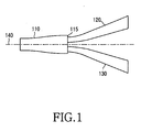
- FIG. 1 diagrammatically illustrates a Y-branch waveguide.
- the Y-branch waveguide includes an input waveguide 110 whose input edge receives optical signals and whose width is gradually larger from the input edge to an output side edge 115, and a first and a second output waveguides 120 and 130 that are symmetrically extended around a central line 140 from the input waveguide 110 to the output side edge 115.
- the Y-branch waveguide is a planar lightwave circuit and is formed by layering a core having a high refractive index and clad having a low refractive index to encompass the core upon a semiconductor substrate.
- the power of the combined optical signals through the input side edge of the Y-branch waveguide splits and is outputted through the first and the second output waveguides 120 and 130. It is important to make the power of the optical signals outputted from the first and the second output waveguides 120 and 130 equal, that is, to make the power split ratio uniform for the Y-branch waveguide. In addition, the power uniformization is required for optical signals of a single channel as well as optical signals of multi-channels.
- FIG. 2a is a diagram illustrating mode profiles of the input waveguide 110 according to a wavelength, on the basis of the output side edge 115 of the input waveguide 110.
- FIG. 2b is a diagram illustrating mode profiles of the first and the second output waveguides 120 and 130 according to a wavelength on the basis of the output side edge 115 of the input waveguide 110.
- FIG. 2a Depicted in FIG. 2a are a first mode profile 210 for a first channel, and a second mode profile 220 for a second channel.
- the first channel has a wavelength of 1250nm
- the second channel has a wavelength of 1650nm.
- the first mode profile 210 for a short wavelength is sharper than the second mode profile 220 for a long wavelength.
- FIG. 2b shows a third mode profile 230 for the first channel and a fourth mode profile 240 for the second channel.
- the third mode profile 230 for a short wavelength is sharper than the fourth mode profile 240 for a long wavelength.
- FIG. 3a is a diagram explaining mode inconsistency of the Y-branch waveguide for the first channel -and FIG. 3b is a diagram explaining mode inconsistency of the Y-branch waveguide for the second channel.
- FIG.s 3a Depicted in FIG.s 3a are the first mode profile 210 of the input waveguide 110 for the first channel and the third mode profile 230 of the first and the second output waveguides 120 and 130. As shown in the drawing, the first mode profile 210 and the third mode profile 230 are not consistent with each other. As a result, this mode inconsistency causes the output of the split optical signals to the first and the second output waveguides 120 and 130.
- FIG. 3b shows the second mode profile 220 of the input waveguide 110 for the second channel and the fourth mode profile 240 of the first and the second output waveguides 120 and 130.
- the second mode profile 220 and the fourth mode profile 240 are not consistent with each other. As a result, this inconsistency causes the output of the split optical signals to the first and the second output waveguides 120 and 130.
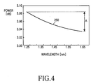
- FIG. 4 is an explanatory diagram of outputs per wavelength in the Y-branch waveguide.
- FIG. 4 shows output curves 250 per wavelength of the first or second output waveguide 110 or 130. As shown in FIG 4, the output power decreases as the wavelength increases. Moreover, the variation range A also increases as the wavelength increases.
- FIG. 5 is a schematic diagram of a prior art-star coupler.
- the star coupler includes an input waveguide 310 for receiving optical signals through an input side edge, an oval-shaped slab waveguide 320 that is connected to the input waveguide 310, and the first through the fourth output waveguides 330, 340, 350 and 360 that are extended symmetrically around a central line 370 from an output side edge 325 of the slab waveguide 320.
- the star coupler is a planar lightwave circuit, and is formed by layering a core having a high refractive index and clad having a low refractive index to encompass the core upon a semiconductor substrate.
- the combined optical signals through the input side edge of the input waveguide 310 are outputted through the first through the fourth output waveguides 330, 340, 350 and 360 via the slab waveguide 320. It is important to make the power split ratio uniform for the star coupler, thereby allowing the output powers of the optical signals from the first through the fourth output waveguides 330, 340, 350 and 360 to also be uniform. In addition, the power uniformization is required for optical signals of a single channel as well as optical signals of multi-channels.
- FIG. 6a is a diagram illustrating mode profiles of the slab waveguide 320 according to a wavelength, based on the output side edge 325 of the slab waveguide 320.
- FIG. 6b is a diagram illustrating mode profiles of the first through the fourth output waveguides 330, 340, 350 and 360 according to a wavelength, based on the output side edge 325 of the slab waveguide 320.
- FIG. 6a Depicted in FIG. 6a are a first mode profile 410 for a first channel and a second mode profile 420 for a second channel.
- the first channel has a wavelength of 1250nm
- the second channel has a wavelength of 1650nm.
- the first mode profile 410 for a shorter wavelength is sharper than the second mode profile 420 for a longer wavelength.
- FIG. 6b shows a third mode profile 430 for the first channel and a fourth mode profile 440 for the second channel.
- the third mode profile 430 for a shorter wavelength is sharper than the fourth mode profile 440 for a longer wavelength.
- FIG. 7a is a diagram explaining mode inconsistency of the star coupler for the first channel and FIG. 7b is a diagram explaining mode inconsistency of the star coupler for the second channel.
- FIG. 7a Depicted in FIG. 7a is the first mode profile 410 of the slab waveguide 320 for the first channel and the third mode profile 430 of the first through the fourth output waveguides 330, 340, 350 and 360. As shown in the drawing, the first mode profile 410 and the third mode profile 430 are not consistent with each other, and this mode inconsistency causes the split optical signals to be outputted to the first through the fourth output waveguides 330, 340, 350 and 360.
- FIG. 7b shows the second mode profile 420 of the slab waveguide 320 for the second channel and the fourth mode profile 440 of the first through the fourth output waveguides 330, 340, 350 and 360.
- the second mode profile 420 and the fourth mode profile 440 are not consistent with each other and this inconsistency causes the split optical signals to be outputted to the first through the fourth output waveguides 330, 340, 350 and 360.
- the outputs of the first and the fourth output waveguides 330 and 360 are similar to each other, and the outputs of the second and the third output waveguides 340 and 350 are similar to each other.
- the star coupler has a bilaterally symmetrical structure around the central line 370 shown in FIG. 5, and the first and the fourth waveguides 330 and 360 and the second and the third output waveguides 340 and 350, respectively, share similarities with each other.
- the star coupler has known limitations with un-uniform power split ratios and output differences between channels. This inconsistency in the power split ratio and the severe output differences between channels consequently deteriorate the performance of the star coupler.
- FIG. 8 is an explanatory diagram of outputs per wavelength of the star coupler. Depicted in the drawing are a first output curve per wavelength 450 of the first or the fourth output waveguide 330 or 360, and a second output curve per wavelength 460 of the second or the third output waveguide 340 or 350. From the drawing it is shown that the output power of the first output curve per wavelength 450 tends to increase for longer wavelengths, while the output power of the second output curve per wavelength 460 tends to decrease for longer wavelengths. Moreover, the entire variation range B of the first and the second output curves per wavelength 450 and 460 is very large.
- the present invention reduces or overcome many of the above limitations by providing an optical power splitter for maximizing uniformization of the power split ratio, while minimizing the output differences between channels.
- an optical power splitter which includes: a semiconductor substrate, a core on the semiconductor substrate that is used as a transmission medium for optical signals, which are composed of multi-channels according to a wavelength, and a clad for encompassing the core.
- the core includes an input waveguide for receiving an optical signal and a plurality of output waveguides for outputting respective portions of the optical signal (whose power has been split).
- the optical power splitter further includes a rectilinear assistant waveguide coupled between the input waveguide and the plurality of output waveguides, having a predetermined width and length that substantially uniforms the mode profiles of the multi-channels (e.g. the respective portions of the optical signal) that are manifested on the output side edge of the rectilinear assistant waveguide, which multi-channels are thereafter provided to the plurality of output waveguides.
- a rectilinear assistant waveguide coupled between the input waveguide and the plurality of output waveguides, having a predetermined width and length that substantially uniforms the mode profiles of the multi-channels (e.g. the respective portions of the optical signal) that are manifested on the output side edge of the rectilinear assistant waveguide, which multi-channels are thereafter provided to the plurality of output waveguides.
- FIG. 9 is a schematic diagram of an optical power splitter in accordance with a preferred embodiment of the present invention.
- the optical power splitter includes a Y-branch waveguide having an input waveguide 510, an assistant waveguide 520, and a first and a second output waveguide 530 and 540.
- the input waveguide 510 receives optical signals through the input side edge and its width gets broader towards output side edge 515.
- the assistant waveguide 520 is coupled between the input waveguide 510 and the first and the second output waveguides 530 and 540.
- the assistant waveguide 520 has a larger width C than the input waveguide 510, and a designated length D.
- the first and the second output waveguides 530 and 540 are extended symmetrically around a central line 550 from an output side edge 525 of the assistant waveguide 520.
- the Y-branch waveguide is a planar lightwave circuit and is formed by layering a core having a high refractive index and clad having a low refractive index to encompass the core upon a semiconductor substrate.
- the maximum mode field diameter of optical signals that are combined through the input side edge of the input waveguide 510 is extended while passing the assistant waveguide 520.
- the local mode field diameter and phase of the optical signals are continuously changed along with the longitudinal direction of the assistant waveguide 520.
- the mode field diameter indicates the width of a mode profile for the optical signal at an arbitrary position on the assistant waveguide 520.
- the assistant waveguide 520 has a designated length for uniformizing mode profiles based on the output side edge 525.
- the first and second output waveguides 530 and 540 split the power of the inputted optical signals through the output side edge 525 of the assistant waveguide 520, and output the split optical signals.
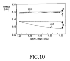
- FIG. 10 is a diagram of the output per wavelength of the Y-branch waveguide.
- Output curve per wavelength 610 is shown for the first or the second output waveguide 530 or 540, where the length of the assistant waveguide 520 is '0'.
- Output curve per wavelength 620 is shown for the first or the second output waveguides 530 or 540, where the length of the assistant waveguide 520 is 225 ⁇ m. It is noted that the width of the assistant waveguide 520 is 12.5 ⁇ m, and if the length of the assistant waveguide 520 is '0', the Y-branch waveguide has the same structure with that of FIG. 1.
- the outputs of the first output curve per wavelength 610 gradually decrease towards longer wavelengths, and the variation range E is relatively large.
- the second output curve per wavelength 620 is uniform, and the variation range F is also relatively small.
- FIG. 11 is a schematic diagram of an optical power splitter in accordance with another embodiment of the present invention. More specifically, FIG. 11 shows a star coupler, which includes an input waveguide 710 for receiving optical signals through an input side edge, an assistant waveguide 620, an oval-shaped slab waveguide 730 and a first through fourth output waveguides 740, 750, 760 and 770.
- a star coupler which includes an input waveguide 710 for receiving optical signals through an input side edge, an assistant waveguide 620, an oval-shaped slab waveguide 730 and a first through fourth output waveguides 740, 750, 760 and 770.
- the assistant waveguide 720 is coupled between the input waveguide 710 and the first and the slab waveguide 730.
- the assistant waveguide 720 has a larger width G than the input waveguide 710, and a designated length H.
- the oval-shaped slab waveguide 730 is coupled to the assistant waveguide 720 and the first through the fourth output waveguides 740, 750, 760 and 770 are extended symmetrically around a central line 780 from an output side edge 735 of the slab waveguide 730.
- the star coupler is a planar lightwave circuit and is formed by layering a core having a high refractive index and clad having a low refractive index to encompass the core upon a semiconductor substrate.
- the maximum mode field diameter of optical signals that are combined through the input side edge of the input waveguide 710 is extended while passing the assistant waveguide 720. Also, the local mode field diameter and phase of the optical signals are continuously changed along with the longitudinal direction of the assistant waveguide 720.
- the assistant waveguide 720 has a designated length for uniformizing mode profiles on the basis of the output side edge 725. Thereafter, the optical signals are outputted through the first through the fourth output waveguides 740, 750, 760 and 770 via the slab waveguide 730.
- FIGs. 12 through 15 are diagram of the output changes of the star coupler according to changes in width G or length H of the assistant waveguide depicted 720.
- FIG. 12 illustrates a case where the width of the assistant waveguide 720 is 9 ⁇ m.
- the drawing shows a first and a second output curves per length 814 and 818 of the first and the second output waveguides 740 and 750 for the first channel, a third and a fourth output curves per length 824 and 828 of the first and the second output waveguides 740 and 750 for the second channel, and a fifth and a sixth output curves per length 834 and 838 of the first and the second output waveguides 740 and 750 for the third channel.
- the first channel has a wavelength of 1250nm
- the first through the sixth output curves per length 814, 818, 824, 828, 834 and 838 have a designated converging region I.
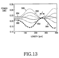
- FIG. 13 illustrates a case where the width of the assistant waveguide 720 is 10 ⁇ m.
- the drawing shows a first and a second output curves per length 844 and 848 of the first and the second output waveguides 740 and 750 for the first channel, a third and a fourth output curves per length 854 and 858 of the first and the second output waveguides 740 and 750 for the second channel, and a fifth and a sixth output curves per length 864 and 868 of the first and the second output waveguides 740 and 750 for the third channel.
- the first channel has a wavelength of 1250nm
- the first through the sixth output curves per length 844, 848, 854, 858, 864 and 868 have a designated converging region J.
- FIG. 14 illustrates a case where the width of the assistant waveguide 720 is 11 ⁇ m.
- the drawing shows a first and a second output curves per length 874 and 878 of the first and the second output waveguides 740 and 750 for the first channel, a third and a fourth output curves per length 884 and 888 of the first and the second output waveguides 740 and 750 for the second channel, and a fifth and a sixth output curves per length 894 and 898 of the first and the second output waveguides 740 and 750 for the third channel.
- the first channel has a wavelength of 1250nm
- the first through the sixth output curves per length 874, 878, 884, 888, 894 and 898 have a designated converging region K.
- FIG. 15 illustrates a case where the width of the assistant waveguide 720 is 12 ⁇ m.
- the drawing shows a first and a second output curves per length 914 and 918 of the first and the second output waveguides 740 and 750 for the first channel, a third and a fourth output curves per length 924 and 928 of the first and the second output waveguides 740 and 750 for the second channel, and a fifth and a sixth output curves per length 934 and 938 of the first and the second output waveguides 740 and 750 for the third channel.
- the first channel has a wavelength of 1250nm
- the first through the sixth output curves per length 914, 918, 924, 928, 934 and 938 have a designated converging region L.
- the assistant waveguide 720 by selecting an optimal length and width for the assistant waveguide 720, it is possible to maximize uniformization of the power split ratio of the star coupler and to minimize differences in outputs between channels thereof.
- FIG. 16 is a diagram of the output per wavelength of the star coupler.
- FIG. 16 illustrates a first and a second output curves per wavelength 940 and 950 for the first and the second output waveguides 740 and 750 in case the length of the assistant waveguide 720 is 0, and a-thirdand a fourth output-curves-per wavelength-960- and 970 for the first and the second output waveguides 740 and 750 in case the assistant waveguide 720 has a width of 11 ⁇ m and a length of 255 ⁇ m. It is noted that when the length of the assistant waveguide 720 is 0, the star coupler has the same structure with that of FIG. 5.
- the output powers on the first output curve per wavelength 940 tend to increase for longer wavelengths, while the output powers on the second output curve per wavelength 950 tend to decrease for longer wavelengths.
- the third and the fourth output curves per wavelength 960 and 970 are uniform. Accordingly, it is found that the variation range N of the third and the fourth output curves per wavelength 960 and 970 is relatively small to the variation range M of the first and the second output curves per wavelength 940 and 950.
- the optical power splitter mounted with the assistant waveguide is beneficial in maximizing the uniformity of the power split ratio and minimizing differences in output between channels by disposing an assistant waveguide having an optimal width and length between an input waveguide and a plurality of output waveguides.
Landscapes
- Physics & Mathematics (AREA)
- General Physics & Mathematics (AREA)
- Optics & Photonics (AREA)
- Engineering & Computer Science (AREA)
- Microelectronics & Electronic Packaging (AREA)
- Optical Integrated Circuits (AREA)
Abstract
Description
In accordance with an embodiment of the present invention an optical power splitter is provided, which includes: a semiconductor substrate, a core on the semiconductor substrate that is used as a transmission medium for optical signals, which are composed of multi-channels according to a wavelength, and a clad for encompassing the core. The core includes an input waveguide for receiving an optical signal and a plurality of output waveguides for outputting respective portions of the optical signal (whose power has been split). The optical power splitter further includes a rectilinear assistant waveguide coupled between the input waveguide and the plurality of output waveguides, having a predetermined width and length that substantially uniforms the mode profiles of the multi-channels (e.g. the respective portions of the optical signal) that are manifested on the output side edge of the rectilinear assistant waveguide, which multi-channels are thereafter provided to the plurality of output waveguides.
Claims (10)
- An optical power splitter comprising:characterized byan input waveguide (510,710),a plurality of output waveguides (530, 540, 740 ,750, 760, 770),
a rectilinear assistent waveguide (520, 720). - An optical power splitter according to claim 1, wherein the input-waveguide (510) is for receiving an optical signal having multi-channels;
and the plurality of output waveguides (530, 540) are for outputting respective portions of the optical signal; and
the rectilinear assistant waveguide (520) has an input edge coupled to the input waveguide (510) and an output edge (525) coupled to the plurality of output waveguides (530, 540), wherein the rectilinear assistant waveguide (520) has a predetermined width (C) and length (D), which substantially enables uniformity of mode profiles of the respective optical signals that are manifested on the output edge (525). - The optical power splitter as claimed in claim 1 or 2, wherein the optical power splitter is fabricated on a semiconductor substrate, having a core layered on the semiconductor substrate, functioning as a transmission medium for optical signals.
- The optical power splitter as claimed in any of claims 1 to 3, wherein the input edge of the assistant waveguide has a width (C) that is larger than the portion of the input waveguide (510) it is coupled to.
- The optical power splitter as claimed in any of claims 1 to 4, wherein the assistant waveguide (520) has a predetermined length to maximize uniformity of mode profiles of the multi-channels manifested on the output edge (525) of the assistant waveguide (520) with a predetermined width (C).
- The optical power splitter according to claim 1, wherein
the input waveguide (510) is for receiving optical signals composed of multi-channels, wherein the optical signal are received by an input side edge that has a larger width towards an output side edge (515);
the plurality of output waveguides (530,540) are a first and a second output waveguides (530, 540), which are extended symmetrically around a central line (550) from an output side edge (515) of the input waveguide (510); and
the rectilinear assistant waveguide (520) is coupled between the input waveguide (510) and the first and the second output waveguides(530, 540), having a designated width (C) and length (D) to uniformize mode profiles of the multi-channels that are manifested on the output side edge (525). - The optical power splitter as claimed in claim 6, wherein an input side edge width (C) of the assistant waveguide (520) is larger than the output side edge width (515) of the input waveguide (510).
- The optical power splitter with an assistance waveguide (520) as claimed in claim 6 or claim 7, wherein the length of the assistant waveguide (520) is designated to maximize uniformity of mode profiles of the multi-channels that are manifested on an output side edge (525) of the assistant waveguide (520) within a pre-designated width (C).
- The optical power splitter according to claim 1 wherein
the input waveguide (710) is for receiving optical signals composed of multi-channels according to a wavelength are inputted through an input side edge; and
the optical power splitter furthermore comprises an oval-shaped slab waveguide (730); and the plurality of output waveguides (740, 750, 760, 770) are extended symmetrically around a central line (780) from an output side edge (735) of the slab waveguide (730); and
the rectilinear assistant waveguide (720) is coupled between the input waveguide (710) and the slab waveguide (730), having a designated length (H) and a larger width (G) than the input waveguide (710). - The optical power splitter according to claim 9, wherein the length of the assistant waveguide (720) is designated to maximize uniformity of mode profiles of the multi-channels that are manifested on an output side edge (725) of the assistant waveguide (720) within a pre-designated width.
Applications Claiming Priority (2)
| Application Number | Priority Date | Filing Date | Title |
|---|---|---|---|
| KR2001079907 | 2001-12-17 | ||
| KR10-2001-0079907A KR100417001B1 (en) | 2001-12-17 | 2001-12-17 | Optical power splitter with assistant waveguide |
Publications (2)
| Publication Number | Publication Date |
|---|---|
| EP1321782A2 true EP1321782A2 (en) | 2003-06-25 |
| EP1321782A3 EP1321782A3 (en) | 2004-11-03 |
Family
ID=19717108
Family Applications (1)
| Application Number | Title | Priority Date | Filing Date |
|---|---|---|---|
| EP02025112A Withdrawn EP1321782A3 (en) | 2001-12-17 | 2002-11-08 | Optical power splitter with assistance waveguide |
Country Status (4)
| Country | Link |
|---|---|
| US (1) | US6904208B2 (en) |
| EP (1) | EP1321782A3 (en) |
| JP (1) | JP2003195076A (en) |
| KR (1) | KR100417001B1 (en) |
Families Citing this family (12)
| Publication number | Priority date | Publication date | Assignee | Title |
|---|---|---|---|---|
| CN102800912B (en) * | 2011-06-29 | 2014-04-16 | 深圳光启高等理工研究院 | Waveguide power divider |
| US9217829B2 (en) | 2012-11-30 | 2015-12-22 | Coriant Advanced Technology, LLC | Compact and low loss Y-junction for submicron silicon waveguide |
| US9778419B1 (en) * | 2016-06-23 | 2017-10-03 | The Boeing Company | Fiber optical system with fiber end face area relationships |
| CN106772803B (en) * | 2016-12-28 | 2019-11-08 | 台州瑜瑞科技有限公司 | Multimode fiber beam splitter and manufacturing method thereof |
| US9946020B1 (en) * | 2017-02-03 | 2018-04-17 | Elenion Technologies, Llc | Mode matched Y-junction |
| CN110646883B (en) * | 2019-09-30 | 2021-04-13 | 华东师范大学重庆研究院 | A three-way silicon-based beam splitter chip and its manufacturing method |
| CN111239895B (en) * | 2020-02-26 | 2020-11-13 | 北京邮电大学 | Waveguide coupling structure and light emitter system |
| US12372724B2 (en) | 2020-09-23 | 2025-07-29 | Apple Inc. | Light splitting device |
| US12487407B2 (en) | 2021-09-24 | 2025-12-02 | Apple Inc. | Compact light splitting devices and methods |
| EP4273599A1 (en) | 2022-05-05 | 2023-11-08 | Apple Inc. | Compact optical splitter |
| US12372719B2 (en) | 2022-09-06 | 2025-07-29 | Apple Inc. | Compact optical coupler |
| CN117075257B (en) * | 2023-09-05 | 2024-07-30 | 南通大学 | A TE0 mode and TE1 mode power divider |
Family Cites Families (12)
| Publication number | Priority date | Publication date | Assignee | Title |
|---|---|---|---|---|
| DE69417986T2 (en) | 1993-11-01 | 1999-09-30 | Sumitomo Electric Industries, Ltd. | Optical branch element |
| US5757995A (en) * | 1995-12-27 | 1998-05-26 | Nhk Spring Co., Ltd. | Optical coupler |
| JPH09178964A (en) * | 1995-12-27 | 1997-07-11 | Nhk Spring Co Ltd | Branching structure for optical waveguide |
| JPH09189817A (en) | 1996-01-09 | 1997-07-22 | Mitsubishi Gas Chem Co Inc | Optical waveguide for optical splitter |
| US5889906A (en) | 1997-05-28 | 1999-03-30 | Lucent Technologies Inc. | Signal router with coupling of multiple waveguide modes for provicing a shaped multi-channel radiation pattern |
| JP3039491B2 (en) * | 1997-11-27 | 2000-05-08 | 日立電線株式会社 | Optical wavelength multiplexer / demultiplexer |
| JP2000171652A (en) * | 1998-12-08 | 2000-06-23 | Showa Electric Wire & Cable Co Ltd | Optical waveguide type optical branching/multiplexing circuit |
| US6195482B1 (en) * | 1998-12-29 | 2001-02-27 | Lucent Technologies Inc. | Waveguide grating router |
| JP3448518B2 (en) * | 1999-07-30 | 2003-09-22 | 古河電気工業株式会社 | Array waveguide diffraction grating |
| US6374013B1 (en) | 1999-12-23 | 2002-04-16 | Nortel Networks Limited | Optical arrayed waveguide grating devices |
| KR100416997B1 (en) * | 2001-07-23 | 2004-02-05 | 삼성전자주식회사 | Y-branch optical waveguide and multi-stage optical power splitter using that |
| US6714704B2 (en) * | 2001-11-29 | 2004-03-30 | Lightcross, Inc. | Optical component having selected bandwidth |
-
2001
- 2001-12-17 KR KR10-2001-0079907A patent/KR100417001B1/en not_active Expired - Fee Related
-
2002
- 2002-10-15 US US10/270,762 patent/US6904208B2/en not_active Expired - Fee Related
- 2002-11-08 EP EP02025112A patent/EP1321782A3/en not_active Withdrawn
- 2002-12-12 JP JP2002360401A patent/JP2003195076A/en not_active Abandoned
Also Published As
| Publication number | Publication date |
|---|---|
| US6904208B2 (en) | 2005-06-07 |
| KR100417001B1 (en) | 2004-02-05 |
| KR20030049636A (en) | 2003-06-25 |
| US20030113066A1 (en) | 2003-06-19 |
| EP1321782A3 (en) | 2004-11-03 |
| JP2003195076A (en) | 2003-07-09 |
Similar Documents
| Publication | Publication Date | Title |
|---|---|---|
| US11714238B2 (en) | Wavelength division multiplexing filter for multiplexing or demultiplexing using cascaded frequency shaping | |
| JP2628258B2 (en) | Mode conversion element | |
| US10768366B2 (en) | Adiabatic polarization rotator combiner | |
| EP1226461B1 (en) | Phasar with flattened pass-band | |
| KR100416997B1 (en) | Y-branch optical waveguide and multi-stage optical power splitter using that | |
| US8811786B2 (en) | Coupled system multi-core fiber, coupling mode multiplexer and demultiplexer, system for transmission using multi-core fiber and method for transmission using multi-core fiber | |
| EP1426799A2 (en) | Optical demultiplexer, optical multi-/demultiplexer, and optical device | |
| EP0881512A2 (en) | Signal router with coupling of multiple waveguide modes for providing a shaped multi-channel radiation pattern | |
| US6904208B2 (en) | Optical power splitter with assistance waveguide | |
| Lierstuen et al. | 8-channel wavelength division multiplexer based on multimode interference couplers | |
| CA2368945A1 (en) | Optical waveguide device having low insertion loss | |
| KR100311281B1 (en) | Add-drop wavelength filter using mode discrimination couplers and tilted Bragg gratings | |
| FI90597C (en) | Mach-Zehnder interferometer | |
| EP1226675B1 (en) | A device and a method for optical multiplexing/demultiplexing | |
| Khalilzadeh et al. | MMI-based all-optical four-channel wavelength division demultiplexer | |
| JP2001108846A (en) | Waveguide grating router | |
| US20030156795A1 (en) | Optical power splitter | |
| US10809457B2 (en) | Optical circuit element | |
| US6731836B2 (en) | Dispersion compensator | |
| JP2003004959A (en) | Waveguide-type optical multiplexer and multi-wavelength light source using the same | |
| Yehia et al. | Cascaded multimode interference phased array structures for dense wavelength division multiplexing applications | |
| Wei et al. | A novel InP-based 1.31/1.55-µm wavelength demultiplexer with side-port multimode interference coupler | |
| JP2003315575A (en) | Optical multiplexer | |
| Huang et al. | A new design approach to large input/output-number multimode interference (MMI) couplers and its WDM applications | |
| JPH1184153A (en) | Optical waveguide functional element |
Legal Events
| Date | Code | Title | Description |
|---|---|---|---|
| PUAI | Public reference made under article 153(3) epc to a published international application that has entered the european phase |
Free format text: ORIGINAL CODE: 0009012 |
|
| 17P | Request for examination filed |
Effective date: 20021108 |
|
| AK | Designated contracting states |
Designated state(s): AT BE BG CH CY CZ DE DK EE ES FI FR GB GR IE IT LI LU MC NL PT SE SK TR |
|
| AX | Request for extension of the european patent |
Extension state: AL LT LV MK RO SI |
|
| PUAL | Search report despatched |
Free format text: ORIGINAL CODE: 0009013 |
|
| AK | Designated contracting states |
Kind code of ref document: A3 Designated state(s): AT BE BG CH CY CZ DE DK EE ES FI FR GB GR IE IT LI LU MC NL PT SE SK TR |
|
| AX | Request for extension of the european patent |
Extension state: AL LT LV MK RO SI |
|
| RIC1 | Information provided on ipc code assigned before grant |
Ipc: 7G 02B 6/125 B Ipc: 7G 02B 6/28 A |
|
| 17Q | First examination report despatched |
Effective date: 20050203 |
|
| AKX | Designation fees paid |
Designated state(s): DE FR GB |
|
| STAA | Information on the status of an ep patent application or granted ep patent |
Free format text: STATUS: THE APPLICATION IS DEEMED TO BE WITHDRAWN |
|
| 18D | Application deemed to be withdrawn |
Effective date: 20061201 |