EP1320191A2 - Transmission output power control device for use in a burst transmitter and control method - Google Patents
Transmission output power control device for use in a burst transmitter and control method Download PDFInfo
- Publication number
- EP1320191A2 EP1320191A2 EP02020819A EP02020819A EP1320191A2 EP 1320191 A2 EP1320191 A2 EP 1320191A2 EP 02020819 A EP02020819 A EP 02020819A EP 02020819 A EP02020819 A EP 02020819A EP 1320191 A2 EP1320191 A2 EP 1320191A2
- Authority
- EP
- European Patent Office
- Prior art keywords
- signal
- rise
- fall
- transmission
- amplitude
- Prior art date
- Legal status (The legal status is an assumption and is not a legal conclusion. Google has not performed a legal analysis and makes no representation as to the accuracy of the status listed.)
- Withdrawn
Links
Images









Classifications
-
- H—ELECTRICITY
- H03—ELECTRONIC CIRCUITRY
- H03G—CONTROL OF AMPLIFICATION
- H03G3/00—Gain control in amplifiers or frequency changers
- H03G3/20—Automatic control
- H03G3/30—Automatic control in amplifiers having semiconductor devices
- H03G3/3036—Automatic control in amplifiers having semiconductor devices in high-frequency amplifiers or in frequency-changers
- H03G3/3042—Automatic control in amplifiers having semiconductor devices in high-frequency amplifiers or in frequency-changers in modulators, frequency-changers, transmitters or power amplifiers
- H03G3/3047—Automatic control in amplifiers having semiconductor devices in high-frequency amplifiers or in frequency-changers in modulators, frequency-changers, transmitters or power amplifiers for intermittent signals, e.g. burst signals
Definitions
- the present invention relates to a transmission output power control device and a transmission output power control method for use in a burst transmitter.
- the cellular phone terminals include so-called dual-mode terminals which have two modulation systems.
- Fig. 20 is a block diagram that shows the configuration of a dual-mode burst transmitter that uses an amplitude modulation system e.g. PDC (Personal Digital Cellular) or CDMA (Code Division Multiple Access), and a constant envelope modulation system, e.g. GSM (Global System for Mobile Communication).
- PDC Personal Digital Cellular
- CDMA Code Division Multiple Access
- GSM Global System for Mobile Communication
- An I/Q signal amplitude control unit 2001 is connected via baseband signal D/A converters 2002 to a modulating unit 2003, and the modulating unit 2003 is connected to a power amplifier 2004 serving as amplifying means.
- the power amplifier 2004 is connected to an antenna 2005 and also to a control voltage signal selecting unit 2007 via a control voltage signal D/A converter 2006.
- the I/Q signal amplitude control unit 2001 includes a waveform data generating portion 2008 and multiplication mixers 2009 connected to each other, and the waveform data generating portion 2008 includes a serial connection of a counter 2010, a table reference number generating portion 2011, and a ramp amplitude waveform data memory 2012.
- the modulating unit 2003 includes a quadrature modulator 2013 and a local oscillator 2014 connected to each other.
- the control voltage signal selecting unit 2007 includes a waveform data control function portion 2015 and a ramp amplitude waveform data memory 2016 connected thereto.
- the configuration operates as shown below.
- Digital baseband signals I and Q are ramped in the I/Q signal amplitude control unit 2001 and then the ramped digital baseband signals I and Q are converted to analog signals in the baseband signal D/A converters 2002.
- Their output amplitude waveform is shown as an analog baseband signal Ia and Qa in Fig. 21A.
- the ramping process performed in the I/Q signal amplitude control unit 2001 will be fully described later.
- the ramped analog baseband signals Ia and Qa are quadrature-modulated in the quadrature modulator 2013 with a high-frequency signal outputted from the local oscillator 2014 and are thus converted to a high-frequency signal to be transmitted.
- the high-frequency signal outputted from the local oscillator 2014 has a frequency that is used in the amplitude modulation system selected by the base station.
- the high-frequency signal to be transmitted is amplified in the power amplifier 2004 and transmitted as a transmission output P from the antenna 2005.
- the control voltage signal selecting unit 2007 receives as its inputs the modulation system signal Sm and a transmission power level signal PCL (0, 1,...
- the waveform data control function portion 2015 causes digital data which corresponds to the modulation system signal Sm and the transmission power level signal PCL to be sent from the ramp amplitude waveform data memory 2016 to the control voltage signal D/A converter 2006.
- the control voltage signal D/A converter 2006 converts the incoming digital data to an analog signal, and during the transmission, it keeps outputting to the power amplifier 2004 a power amplifier control voltage Vc (Vc0 to Vcn) which has a predetermined constant voltage as shown in Fig. 21A. A constant voltage is thus outputted during a burst transmission section.
- the ramp process performed in the I/Q signal amplitude control unit 2001 is described in detail.
- the counter 2010, configured on the basis of a clock, starts counting upon application of a transmission start pulse.
- the table reference number generating portion 2011 specifies table reference numbers, n, for reading I/Q amplitude values Vpiq[n] on a table for use in ramp up.
- the I/Q amplitude values VPiq[n] corresponding to the table reference numbers n are read from the ramp amplitude waveform data memory 2012.
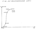
- Fig. 22 shows, in the form of an analog signal, a ramp amplitude waveform VPiq used in the ramping process when the amplitude modulation is selected.
- the ramp amplitude waveform is composed of a collection of data which is required to perform the ramping process.
- a ramp amplitude waveform for ramping the baseband signal is represented as Viq.
- a ramp amplitude waveform for use in the amplitude modulation is represented as VPiq and that for use in the constant envelope modulation is represented as VGiq.
- the ramp up portion exhibits such a waveform as shown in this diagram.
- the values VPiq[n] that form the ramp amplitude waveform VPiq are the I/Q amplitude values that correspond to the table reference numbers n; six values are set herein for the rising ramp process.
- the multiplication mixers 2009 multiplies the I/Q amplitude values VPiq[n] outputted from the waveform data generating portion 2008 and the digital baseband signals I and Q to produce ramped digital baseband signals I and Q.
- nonlinearity is not produced so much between the digital baseband signals I and Q and the transmission output P, so that the I/Q amplitude values VPiq[n] outputted from the waveform data generating portion 2008 can hold a given fixed pattern.
- the constant envelope modulation nonlinear circuitry is often used between the digital baseband signals I, Q and the transmission output P; therefore nonlinearity is produced. Accordingly the ramping process for the transmission output P is performed not in the I/Q signal amplitude control unit 2001 but in the control voltage signal selecting unit 2007 which outputs the control voltage signal Vc for controlling the power amplifier 2004. Therefore the digital baseband signals I and Q are outputted from the I/Q signal amplitude control unit 2001 without undergoing ramp process.
- the digital baseband signals I and Q from the I/Q signal amplitude control unit 2001 are converted to analog signals in the baseband signal D/A converters 2002 and outputted therefrom.
- the outputs exhibit an amplitude waveform having a constant amplitude that rises and falls vertically.
- the analog baseband signals Ia and Qa are quadrature-modulated in the quadrature modulator 2013 in the modulating unit 2003 with the high-frequency signal from the local oscillator 2014, and are thus converted to a high-frequency signal to be transmitted.
- the high-frequency signal outputted from the local oscillator 2014 has a frequency that is used in the constant envelope modulation system selected by the base station.
- the transmission high-frequency signal outputted from the modulating unit 2003 is amplified in the power amplifier 2004 and transmitted as the transmission output P from the antenna 2005.
- the waveform data control function portion 2015 reads a ramp amplitude waveform corresponding to these signals from the ramp amplitude waveform data memory 2016 and outputs the digital control voltage data for that ramp amplitude waveform to the control voltage signal D/A converter 2006 in synchronization with a transmission timing clock.
- the control voltage signal D/A converter 2006 On the basis of the digital data input corresponding to the transmission power level signal PCL, the control voltage signal D/A converter 2006 generates the control voltage Vc (Vc0 to Vcn) for controlling the power amplifier 2004; the control voltage Vc slowly rises and falls as shown in Fig. 21B.
- the control voltage signal D/A converter 2006 then outputs the control voltage Vc to the power amplifier 2004, so as to control the transmission output P into a smooth waveform so that the spectrum will not spread in a wide range.
- the conventional technique realizes the ramping process by controlling the control voltage Vc to the power amplifier 2004.
- the control voltage signal Vc since the characteristics of the power amplifier 2004 differ in different radio devices, it is impossible to initially set a table for controlling the power amplifier, so that the table must be stored in a rewritable storage, i.e. in the memory 2016.
- the control voltage signal Vc when the constant envelope modulation is selected, the control voltage signal Vc must be varied in accordance with the level indicated by the transmission power level signal PCL, and the ramping process must be applied to the varied version of the control voltage signal Vc. Accordingly, it is necessary to store different ramp amplitude waveforms for the control voltage Vc in correspondence with the individual levels of the transmission power level signal PCL. Therefore, a large amount of data must be stored in the ramp amplitude waveform data memory 2016 and the control voltage signal D/A converter 2006 must be controlled each time a transmission is made, which requires an increased amount of processing and increased consumption of power.
- the ramping process must be conducted in different places depending on whether the amplitude modulation is selected or the constant envelope modulation is selected.
- the modulation systems require their respective ramp amplitude waveform data memories and their respective operation procedures, which also requires increased consumption of power.
- a first object of the present invention is, in a burst transmitter using a constant envelope modulation, to reduce the amount of memory, the amount of processing, and the consumption of power required for a ramp process to the transmission output power.
- a second object of the invention is to perform the ramp process in such a way as to more effectively suppress the spreading of the spectrum of the transmission output power.
- a third object of the invention is to reduce the amount of processing and the consumption of power and to suppress the spreading of the spectrum.
- a transmission output power control device in a burst transmitter using a constant envelope modulation system, includes an I/Q signal amplitude control portion, a modulator, an amplifier, and control voltage signal selecting means.
- the I/Q signal amplitude control portion variably controls the shape of a rise and a fall of the waveform of a baseband signal and its burst transmission time from the end of the rise to the beginning of the fall.
- the modulator modulates the baseband signal controlled in the I/Q signal amplitude control portion into a high-frequency signal for transmission.
- the amplifier amplifies the transmission high-frequency signal modulated in the modulator.
- the control voltage signal selecting means outputs a predetermined constant voltage which is determined by a transmission power level signal, so as to control an output power of the amplifier.
- a burst transmitter using a constant envelope modulation In a burst transmitter using a constant envelope modulation, the shape of a rise and a fall of the waveform of the baseband signal and its burst transmission time from the end of the rise to the beginning of the fall are variably controlled. This eliminates the need for ramp process to the control voltage to the power amplifier and reduces the amount of memory, the amount of processing or the consumption of power, and provides a burst transmitter using a constant envelope modulation in which the spreading of spectrum resulting from the magnitude of the transmission output power can be suppressed during the transmission.
- a transmission output power control device in a dual-mode burst transmitter using a constant envelope modulation system and an amplitude modulation system, includes an I/Q signal amplitude control portion, a modulator, an amplifier, and control voltage signal selecting means.
- the I/Q signal amplitude control portion variably controls the shape of a rise and a fall of the waveform of a baseband signal and its burst transmission time from the end of the rise to the beginning of the fall.
- the modulator modulates the baseband signal controlled in the I/Q signal amplitude control portion into a transmission high-frequency signal in accordance with the modulation system signal.
- the amplifier amplifies the transmission high-frequency signal modulated in the modulator.
- the control voltage signal selecting means outputs a predetermined constant voltage which is determined by the modulation system signal and a transmission power level signal, so as to control an output power of the amplifier.
- the envelope of the transmission output power is controlled by controlling the baseband signal no matter which of the modulation systems is used. Furthermore, the burst transmission time is variable. This eliminates the need for provision of separate control devices for ramping the transmission output power in the individual modulation systems and reduces the amount of memory, the amount of processing or the consumption of power. Also, the spreading of spectrum due to the length of the burst transmission time can be suppressed during the transmission.
- a transmission output power control device in a dual-mode burst transmitter using a constant envelope modulation system and an amplitude modulation system, includes an I/Q signal amplitude control portion, a modulator, an amplifier, a detector, and a signal processing portion.
- the I/Q signal amplitude control portion variably controls the shape of a rise and a fall of the waveform of a baseband signal and its burst transmission time from the end of the rise to the beginning of the fall.
- the modulator modulates the baseband signal controlled in the I/Q signal amplitude control portion into a high-frequency signal for transmission in accordance with the modulation system signal.
- the amplifier amplifies the transmission high-frequency signal modulated in the modulator.
- the detector detects a transmission output power outputted from the amplifier.
- the signal processing portion outputs a control voltage to the amplifier in accordance with a signal from the detector in such a way as to make the transmission output power attain a target output power, obtains a difference between a target control voltage and the control voltage with which the transmission output power of the amplifier attained the target output power, and controls the I/Q signal amplitude control portion so that the shape of the rise and the fall of the waveform of the baseband signal and its burst transmission time from the end of the rise to the beginning of the fall are varied on the basis of the difference.
- the transmission output power of the amplifier is detected and fed back.
- the nonlinearity of the amplifier can be estimated and the ramp process to the baseband signal can be performed on the basis of the estimated nonlinearity.
- the spreading of spectrum due to the nonlinearity of the amplifier can thus be suppressed during the transmission.
- the envelope of an output power for transmission is controlled by variably controlling the shape of a rise and a fall of the waveform of a baseband signal and its burst transmission time from the end of the rise to the beginning of the fall.
- the envelope of the transmission output power is controlled by variably controlling the shape of a rise and a fall of the waveform of the baseband signal and its burst transmission time from the end of the rise to the beginning of the fall. This reduces the amount of memory, the amount of processing or the consumption of power required to ramp the transmission output power of the burst transmitter, and the spreading of spectrum can be suppressed during the transmission.
- the envelope of an output power for transmission is controlled by variably controlling the shape of a rise and a fall of the waveform of a baseband signal and its burst transmission time from the end of the rise to the beginning of the fall.
- the envelope of the transmission output power is controlled by variably controlling the shape of a rise and a fall of the waveform of the baseband signal and its burst transmission time from the end of the rise to the beginning of the fall. This reduces the amount of memory, the amount of processing or the consumption of power required to ramp the transmission output power of the burst transmitter, and the spreading of spectrum can be reduced during the transmission.
- Fig. 1 is a block diagram that shows a dual-mode burst transmitter according to a first preferred embodiment; the dual-mode burst transmitter uses an amplitude modulation system and a constant envelope modulation system (e.g. the PDC system and the GSM system).
- the baseband signal D/A converters 2002, the modulating unit 2003, the power amplifier 2004, the antenna 2005, the control voltage signal D/A converter 2006, and the multiplication mixers 2009 are the same as those described in Background Art.
- the reference numeral 101 shows an I/Q signal amplitude control unit which includes a waveform data generating portion 103 and the multiplication mixers 2009, where the waveform data generating portion 103 includes a counter 104, a table reference number generating portion 105, and a ramp amplitude waveform data memory 106.
- the waveform data generating portion 103 receives as its inputs a modulation system signal Sm, a clock signal, and a transmission start pulse.
- the I/Q signal amplitude control unit 101 has a function of varying the rising and falling waveform of the baseband signals and their effective data transmission section Tb from the end of the rise to the beginning of the fall according to the modulation system, so that the ramping process can be performed in the I/Q signal amplitude control unit irrespective of which modulation system is selected.
- the effective data transmission section Tb will be fully described later.
- the reference numeral 102 shows a control voltage signal selecting unit which, during transmission, outputs digital data for the control voltage Vc to the power amplifier 2004 in accordance with the input modulation system signal Sm and the transmission power level signal PCL; the control voltage signal selecting unit 102 contains a nonvolatile memory etc.
- the control voltage signal selecting unit 102 can be realized by reading digital control voltage data stored in a nonvolatile memory. In this case it is not necessary to ramp the control voltage signal Vc, so that the space for storing the collection of digital voltage data required for the ramping process can be reduced as compared with that in the conventional example.
- the control voltage signal selecting unit 102 can also be realized by using a processor.
- the ramped digital baseband signals I and Q are converted to analog signals in the baseband signal D/A converters 2002.
- the quadrature modulator 2013 quadrature-modulates the converted analog baseband signals Ia and Qa with a high-frequency signal outputted from the local oscillator 2014 to generate a high-frequency signal to be transmitted.
- the high-frequency signal outputted from the local oscillator 2014 has a frequency that is used in the modulation system selected by the base station.
- the high-frequency signal to be transmitted is amplified in the power amplifier 2004 and transmitted as a transmission output P from the antenna 2005.
- the control voltage signal selecting unit 102 receives as its inputs the modulation system signal Sm and the transmission power level signal PCL, and the control voltage signal selecting unit 102 sends digital control voltage data corresponding to the transmission power level signal PCL to the control voltage signal D/A converter 2006.
- the control voltage signal D/A converter 2006 converts the digital control voltage data to an analog signal and outputs it, and the output analog signal controls the power amplifier 2004 as the control voltage signal Vc.
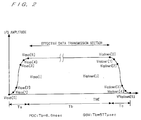
- Fig. 2 is a diagram that shows the amplitude waveform of the analog baseband signal which has been ramped in the I/Q signal amplitude control unit 101 and converted to an analog signal. While the analog baseband signals Ia and Qa which are not ramped show a rectangular waveform having a vertical rise and a vertical fall, the ramped analog baseband signals Ia and Qa are corrected to exhibit a waveform which gently and slowly rises and falls.
- the time required for rise is referred to as a ramp up time Ta
- the time from the end of the rise to the beginning of the fall is referred to as an effective data transmission time Tb
- the time required for fall is referred to as a ramp down time Tc.
- the effective data transmission section Tb has a sufficient height and a constant voltage and hence is capable of effectively sending data; the effective data transmission section Tb corresponds to the burst transmission time of the burst transmitter of this invention.
- the burst transmission time must approximately be equal to the value of the burst transmission time determined by the modulation system.
- the burst transmission time is determined to be about 6.6 msec (at full rate) in the PDC system, an amplitude modulation system, and to be about 577 ⁇ sec (at full rate) in the GSM system, a constant envelope modulation system.
- the effective data transmission section Tb must be varied depending on the modulation system.
- the effective data transmission section Tb corresponds to the time in which the I/Q amplitude value Viq[n] of the analog baseband signals Ia and Qa is achieving a prescribed voltage.
- the time in which the prescribed voltage is being achieved should not last unnecessarily long, since the spectrum will spread if this time lasts too long.
- the I/Q signal amplitude control unit 101 has a function for causing the effective data transmission section Tb to vary depending on the modulation system.
- Fig. 3 is a diagram that illustrates signal timing in the ramp process to the digital baseband signals I and Q; for comparison between the process in the amplitude modulation and that in the constant envelope modulation, the diagram shows up and down start waveforms Sp and Sg, table reference numbers, np and ng, and I/Q amplitude values VPiq[n] and VGiq[n] that are used in the amplitude modulation system and the constant envelope modulation system.
- the counter 104 starts counting up its value T in response to the transmission start pulse.
- the up and down start pulse Sp rises.
- the table reference number generating portion 105 specifies a table for use in the amplitude modulation and specifies table reference numbers, np, for reading the I/Q amplitude values VPiq[n] on the table.
- np a number appropriate for use in the amplitude modulation system (five in this example)
- np a number appropriate for use in the amplitude modulation system (five in this example)
- the table reference number np is then fixed until the up and down start pulse Sp falls.
- an appropriate number of table reference numbers np are specified again.
- the I/Q amplitude values VPiq[n] used for ramp up are also used for ramp down.
- the I/Q amplitude values VPiq[0] to VPiq[5] are read from the ramp amplitude waveform data memory 106. Also, when the table reference number np varies from 5 to 0 as shown in this diagram, the I/Q amplitude values VPiq[5] to VPiq[0] are read from the ramp amplitude waveform data memory 106.
- the multiplication mixers 2009 multiply the I/Q amplitude values VPiq[n] outputted from the waveform data generating portion 103 and the digital baseband signals I and Q to produce the ramped digital baseband signals I and Q.
- the counter 104 configured on the basis of the clock starts counting.
- the table reference number generating portion 105 specifies a table for use in the constant envelop modulation and specifies table reference numbers ng for reading the I/Q amplitude values VGiq[n] on the table.
- table reference numbers ng i.e., a number appropriate for use in the constant envelope modulation (seven in this example), are specified, and the table reference number ng is then fixed until the up and down start pulse Sp falls. When the up and down start pulse Sg falls, then an appropriate number to table reference numbers ng are specified again.
- the same I/Q amplitude values VGiq[n] are used for ramp up and ramp down.
- the table reference number ng varies from 0 to 7 as shown in this diagram
- the I/Q amplitude values VGiq[0] to VGiq[7] are read from the ramp amplitude waveform data memory 106.
- the table reference number ng varies from 7 to 0 as shown in this diagram, the I/Q amplitude values VGiq[7] to VGiq[0] are read from the ramp amplitude waveform data memory 106.
- the I/Q amplitude value Viq[n] corresponds to the table reference number n; six I/Q amplitude values VPiq[n] are set for the rising ramp and eight I/Q amplitude values VGiq[n] are set for the rising ramp. A larger number of values (a larger number of values Viq[n]) are thus set in the constant envelope modulation than in the amplitude modulation. Also, the up and down start pulse Sg for the constant envelope modulation is shorter than the up and down start pulse Sp for the amplitude modulation. This lengthens the ramp up section Ta and the ramp down section Tc and shortens the effective data transmission section Tb. In this way, the effective data transmission section Tb can be varied by varying the number of n.
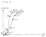
- Fig. 4 shows, in the form of analog signals, the ramp amplitude waveforms Viq stored in correspondence with the respective modulation systems in the ramp amplitude waveform data memory 106.
- the ramp up portions exhibit amplitude waveforms as shown in this diagram.
- the ramp amplitude waveform used for the amplitude modulation is represented by VPiq5 including the I/Q amplitude values VPiq[0] to VPiq[5]
- the ramp amplitude waveform used for the constant envelope modulation is represented by VGiq7 including the I/Q amplitude values VGiq[0] to VGiq[7].
- Viqup[i] Viq ⁇ [1-COS ⁇ ( ⁇ /T) ⁇ ( ⁇ t ⁇ i) ⁇ ]
- Viqdown[j] Viqup [imax-j]
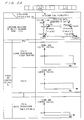
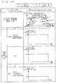
- Figs. 5A and 5B show, in the upper section, the amplitude waveforms of the analog baseband signals Ia and Qa that are ramped as shown above in the I/Q amplitude control unit 101 according to the amplitude modulation and constant envelope modulation systems, respectively.
- control voltage Vc is described referring to the lower sections in Figs. 5A and 5B; the control voltage Vc is controlled in the control voltage signal selecting unit 102 on the basis of the modulation system signal and the transmission power level signal PCL.
- the control voltage signal selecting unit 102 selects a small constant voltage as the control voltage Vc.
- a large power is needed for the transmission output P, so that the control voltage Vc0 involves a large constant voltage.
- the control voltage signal D/A converter 2006 converts the input digital control voltage data into the control voltage Vc in the form of an analog signal and continuously outputs the constant voltage during the transmission. Note that, as compared with the control voltage Vc to the power amplifier 2004 required in the amplitude modulation system, the control voltage Vc used in the constant envelope modulation system is higher for a reason related to the system. While it is assumed herein that a larger control voltage Vc0 provides the transmission output P with a larger power, it depends on the characteristics of the transmission power amplifier 2004. A smaller control voltage Vc0 may provide the transmission output P with a larger power.
- the control voltage Vc to the power amplifier 2004 exhibits a predetermined constant voltage value.
- the present invention thus allows the control voltage signal selecting unit 102 to be constructed in a simplified manner.
- the digital baseband signals I and Q are ramp-processed whichever of the modulation systems is used (amplitude modulation or constant envelope modulation) to ramp-process the transmission output.
- amplitude modulation or constant envelope modulation amplitude modulation or constant envelope modulation
- Fig. 6 is a block diagram showing a dual-mode burst transmitter which uses an amplitude modulation system and a constant envelope modulation system (e.g. PDC and GSM) according to a second preferred embodiment.
- the reference numeral 601 denotes an I/Q signal amplitude control unit including a waveform data generating portion 602 and the multiplication mixers 2009, where the waveform data generating portion 602 includes a counter 603, a table reference number generating portion 604, and a ramp amplitude waveform data memory 605.
- This structure differs from that of the first preferred embodiment in that the transmission power level signal PCL is given to the waveform data generating portion 602 so that the nonlinearity produced between the digital baseband signals I and Q and the transmission output P can be considered to suppress the spreading of the spectrum.
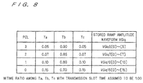
- the ramp amplitude waveform data memory 605 as shown in Fig. 8, the rise time Ta and the fall time Tc of the baseband signals are set in correspondence with the levels of the transmission power level signal PCL. Accordingly, as compared with the table reference number generating portion 105, the table reference number generating portion 604 performs its processing on the basis of a more variety of conditions. In other respects the configuration is the same as that of the first preferred embodiment and therefore not described again.
- the digital baseband signals I and Q are ramped in the I/Q signal amplitude control unit 601 and the ramped digital baseband signals I and Q are converted to analog baseband signals Ia and Qa in the baseband signal D/A converters 2002.
- the quadrature modulator 2013 quadrature-modulates the analog baseband signals Ia and Qa with the high-frequency signal outputted from the local oscillator 2014 to produce a high-frequency signal for transmission.
- the high-frequency signal outputted from the local oscillator 2014 has a frequency that is used in the amplitude modulation system selected by the base station.
- the high-frequency signal for transmission is amplified in the power amplifier 2004 and transmitted from the antenna 2005 as the transmission output P.
- the control voltage signal D/A converter 2006 converts the digital control voltage data to an analog signal and outputs it, and this analog signal controls the power amplifier 2004 as the control voltage Vc.
- Fig. 7 shows the linearity of the analog baseband signals Ia and Qa and the transmission output P and the spreading of the spectrum which are exhibited when the ramp process to the transmission output P is achieved by ramping the digital baseband signals I and Q.
- the spectrum does not spread when the power amplifier 2004 is operating in the linear region.
- the power amplifier 2004 operates in the nonlinear region (e.g.
- the ramp up and the ramp down of the transmission output P do not smoothly vary if the I/Q signal amplitude control unit 601 provides a fixed pattern of waveform, which causes the spectrum to spread in a wider range.
- This preferred embodiment aims to solve this problem which takes place when the envelope of the transmission output P is ramped by ramping the digital baseband signals I and Q.
- Fig. 8 shows the ramp amplitude waveforms VGiq to be stored in the ramp amplitude waveform data memory 605 in this preferred embodiment and the values of Ta, Tb and Tc at the individual levels of the transmission power level signal PCL, where the transmission slot time is assumed to be 1.00.
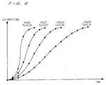
- Fig. 9 shows the ramp amplitude waveforms VGiq shown in Fig. 8 as analog waveforms.
- Figs. 8 and 9 four combinations of times are prepared in correspondence with the levels indicated by the transmission power level signal PCL, which range from the ramp amplitude waveform VGiq5 having the shortest ramp up section Ta to the ramp amplitude waveform VGiq15 having the longest ramp up section Ta.
- the ramp amplitude waveforms VGiq which exhibit the waveforms shown in Fig. 9 when converted into analog form, an optimum ramp amplitude waveform VGiq is selected on the basis of the modulation system signal Sm and the transmission power level signal PCL, and this ramp amplitude waveform VGiq and the digital baseband signals I and Q are multiplied together.
- the I/Q amplitude values Vgiq[n] used in the ramp up process are also used in the ramp down process in the reverse order, i.e. the I/Q amplitude value VGiqup[i] that is used as the ith value in ramp up is used as the backwardly counted ith value in ramp down, so that only the I/Q amplitude values [n] used for the ramp up are stored in the ramp amplitude waveform data memory 605.
- the number of points VGiq[n] on the waveforms shown in Fig. 9 differs depending on the level indicated by the transmission power level signal PCL. Using a larger number of values VGiq[n] increases the ramp up time Ta and makes the rise slower.
- the control voltage Vc is higher, the nonlinearity in the relation between the digital baseband signals I, Q and the transmission output P is stronger.
- the I/Q amplitude can be controlled most favorably in accordance with the level indicated by the transmission power level signal PCL.
- the spreading of the spectrum can be easily prevented even when the power amplifier 2004 operates in a nonlinear region.
- a third preferred embodiment differs from the second preferred embodiment in that the ramp amplitude waveform data memory 605 separately stores the I/Q amplitude values Viq[n] for use in the ramp up process and those for use in the ramp down process.
- Fig. 10 shows a waveform of the analog baseband signals Ia and Qa that is obtained in the I/Q signal amplitude control unit used in this invention, where the horizontal axis shows the time and the vertical axis shows the I/Q amplitude.
- the waveform of the transmission output is not symmetrical on the time base but is ramped up so that the waveform swells up and ramped down so that the waveform caves in. It is thought that controlling the amplitude waveform in this way suppresses the spreading of the spectrum.
- the third preferred embodiment enables the ramp process to more effectively suppress the spectrum spreading than the second preferred embodiment.
- the digital baseband signals I and Q are ramped in the I/Q signal amplitude control unit 601 and converted to analog signals in the baseband signal D/A converters 2002.
- the I/Q amplitude values VPiq[n] used for ramp up and those used for ramp down are separately stored in the ramp amplitude waveform data memory 605. In other respects the operation is the same as that of the second preferred embodiment and therefore not described again.
- the digital baseband signals I and Q are ramped in the I/Q signal amplitude control unit 601 and converted to analog signals in the baseband signal D/A converters 2002.
- the I/Q amplitude values VGiq[n] used for ramp up and those used for ramp down are separately, and in correspondence with the levels of the transmission power level signal PCL, stored in the ramp amplitude waveform data memory 605.
- the operation is the same as that of the second preferred embodiment and therefore not described again.
- the spreading of the spectrum can be more effectively suppressed even when the power amplifier 2004 operates in the nonlinear region.
- Fig. 11 shows a dual-mode burst transmitter of a fourth preferred embodiment; the dual-mode burst transmitter uses an amplitude modulation system and a constant envelope modulation system (e.g. PDC and GSM).
- the reference numeral 1106 denotes a temperature detecting circuit for detecting the ambient temperature of the power amplifier 2004.
- the temperature detecting circuit 1106, provided near the power amplifier 2004, includes a thermistor 1107 whose resistance value varies with change in temperature, a resistor 1108 connected in series with the thermistor 1107, and a temperature measuring A/D converter 1109 connected to the connection point between the thermistor 1107 and the resistor 1108.
- the reference numeral 1101 denotes an I/Q signal amplitude control unit including a waveform data generating portion 1102 and the multiplication mixers 2009.
- the waveform data generating portion 1102 of this preferred embodiment like that of the second preferred embodiment, includes a counter 1103, a table reference number generating portion 1104, and a ramp amplitude waveform data memory 1105.
- the waveform data generating portion 1102 receives as its input the temperature information from the temperature detecting circuit 1106, as well as the modulation system signal Sm and the transmission power level signal PCL.
- the ramp amplitude waveform data memory 1105 stores a plurality of ramp amplitude waveforms VGiq so that the rise time Ta and the fall time Tc of the baseband signals can be selected in accordance with the modulation system signal Sm, the transmission power level signal PCL, and the temperature information. Accordingly, as compared with the table reference number generating portion 604, the table reference number generating portion 1104 in the waveform data generating portion 1102 operates on the basis of a more variety of conditions. As for the temperature detecting circuit 1106 shown in Fig. 11, a processor etc., e.g.
- a CPU may be connected in a stage that follows the temperature measuring A/D converter 1109, and then, for example, the temperature can be measured several times and the digital data can be averaged before being fed to the waveform data generating portion 1102.
- the configuration is the same as that shown in Fig.6 of the second preferred embodiment and therefore not described again.
- the power amplifier 2004 operates at high output power and therefore it generates heat when the transmission lasts long in time. Also, the temperature varies depending on the environment where the radio transmitter is used. In such a case, the distortion characteristic varies in accordance with the temperature characteristic of the power amplifier 2004 and then the transmission output P cannot be slowly ramped up and down, causing the spreading of the spectrum. It is therefore necessary to consider the temperature of the power amplifier 2004 during operation.
- a power-supply voltage controlled to be a constant voltage is divided between the thermistor 1107 and the resistor 1108 and the output voltage value is converted to digital data in the temperature detecting A/D converter 1109, which is sent to the waveform data generating portion 1102; the temperature can thus be detected.
- an optimum ramp amplitude waveform Viq is selected as the waveform of the analog baseband signals Ia and Qa which are ramped on the basis of the temperature information from the temperature detecting circuit 1106.
- Fig. 12 shows ramp amplitude waveforms VGiq that can be selected on the basis of the temperature information when the constant envelope modulation is used and the transmission power level signal PCL indicates level 2, where the values of Ta, Tb and Tc are shown with the transmission slot time assumed to be 1.00.
- the stored ramp amplitude waveforms VGiq include four groups of waveforms in accordance with the transmission power level signal PCL and each group includes three versions in accordance with the temperature information; 12 ramp amplitude waveforms VGiq are thus stored.
- the temperature is higher, the nonlinearity of the power amplifier 2004 is stronger, so that the rise time Ta and the fall time Tc are set longer than when the temperature is lower so as to cause the waveform to rise and fall slowly, thereby preventing the spreading of spectrum.
- this diagram shows an example in the case of the constant envelope modulation, the distortion due to temperature occurs also when the amplitude modulation is used.
- the ramping process can be performed in a fixed way irrespective of the transmission power level signal PCL. Accordingly, the ramp process may include three levels depending on the temperature information, using three sets of stored ramp amplitude waveforms VPiq. In other respects the operation is the same as that of the second preferred embodiment and therefore not described again.
- Fig. 13 shows a dual-mode burst transmitter according to a fifth preferred embodiment; the dual-mode burst transmitter uses an amplitude modulation system and a constant envelope modulation system (e.g. PDC and GSM).
- the reference numeral 1306 denotes a power-supply voltage detecting circuit for detecting the voltage of the battery, i.e. the power-supply voltage.
- the power-supply voltage detecting circuit 1306 includes a power-supply battery 1307 and a power-supply voltage A/D converter 1308.
- the reference numeral 1301 indicates an I/Q signal amplitude control unit which includes a waveform data generating portion 1302 and the multiplication mixers 2009.
- the waveform data generating portion 1302 like that of the second preferred embodiment, includes a counter 1303, a table reference number generating portion 1304, and a ramp amplitude waveform data memory 1305.
- the waveform data generating portion 1302 receives as its input the power-supply voltage information from the power-supply voltage detecting circuit 1306, as well as the modulation system signal Sm and the transmission power level signal PCL.
- the ramp amplitude waveform data memory 1305 stores a plurality of ramp amplitude waveforms Viq so that the rise time Ta and the fall time Tc of the analog baseband signals Ia and Qa can be selected in accordance with the modulation system signal Sm, the transmission power level signal PCL, and the power-supply voltage information.
- the table reference number generating portion 1304 in the waveform data generating portion 1302 operates on the basis of a more variety of conditions.
- the digital power-supply voltage information may be averaged in a processor, e.g. a CPU, and then fed to the waveform data generating portion 1302, for example.
- the configuration is the same as that shown in Fig. 6 of the second preferred embodiment and therefore not described again.
- the power-supply for the power amplifier 2004 is often directly supplied from the battery in order to efficiently output the transmission output P.
- the battery voltage greatly varies depending on the amount of the remaining electricity.
- the distortion characteristic varies in accordance with the power-supply voltage characteristic of the power amplifier, and then the transmission output P cannot exhibit a smooth waveform, leading to the spreading of spectrum. It is therefore necessary to consider the power-supply voltage information.
- the power-supply voltage detecting circuit 1306 is described.
- the power-supply voltage is detected by converting an analog voltage value of the battery 1307 into digital data in the power-supply voltage A/D converter 1308.
- the signal thus detected is fed to the waveform data generating portion 1302.
- an optimum ramp amplitude waveform Viq is selected on the basis of the voltage information from the power-supply voltage detecting circuit 1306.
- Fig. 14 shows ramp amplitude waveforms VGiq that can be selected on the basis of the power-supply voltage information when the constant envelope modulation is used and the transmission power level signal PCL indicates level 2.
- Fig. 14 shows ramp amplitude waveforms VGiq that can be selected on the basis of the power-supply voltage information when the constant envelope modulation is used and the transmission power level signal PCL indicates level 2.
- the stored ramp amplitude waveforms VGiq include four groups of waveforms in accordance with the transmission power level signal PCL and each group includes three versions in accordance with the power-supply voltage information; 12 ramp amplitude waveforms VGiq are thus stored. While this diagram shows an example in the case of the constant envelope modulation, such distortion occurs in the same way in the amplitude modulation when a burst transmitter using battery voltage is used.
- the ramp process can be performed in a fixed way irrespective of the transmission power level signal PCL. Accordingly, the ramp process may involve three levels depending on the power-supply voltage information, using three sets of stored ramp amplitude waveforms VPiq. In other respects the operation is the same as that of Fig. 6 shown in the second preferred embodiment and therefore not described again.
- Fig. 15 is a block diagram showing a dual-mode burst transmitter according to a sixth preferred embodiment; the dual-mode burst transmitter uses an amplitude modulation system and a constant envelope modulation system (e.g. PDC and GSM).
- the reference numeral 1501 denotes an electric matching adjusting circuit connected in the stage that precedes the power amplifier 2004; when the nonlinearity in the burst transmitter becomes stronger during the amplitude modulation or constant envelope modulation, the electric matching adjusting circuit 1501 corrects it.
- the reference numeral 1501 denotes an electric matching adjusting circuit connected in the stage that precedes the power amplifier 2004; when the nonlinearity in the burst transmitter becomes stronger during the amplitude modulation or constant envelope modulation, the electric matching adjusting circuit 1501 corrects it.
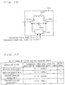
- the electric matching adjusting circuit 1501 includes a select signal generating portion 1601 receiving the modulation system signal Sm and the transmission power level signal PCL and generating a select signal, a parallel circuit of a coil 1602 and a capacitor 1604, and switches 1603 for switching between the coil and the capacitor with the select signal.
- the select signal may be generated in a processor, e.g. a CPU. While the electric matching adjusting circuit 1501 is connected in a stage that precedes the power amplifier 2004 in the diagram, it may be connected in a stage that follows the power amplifier 2004. In other respects the configuration is the same as that shown in Fig. 1 of the first preferred embodiment and therefore not described again.
- the digital baseband signals I and Q are ramped in the I/Q signal amplitude control unit 101 and are converted to analog signals in the baseband signal D/A converters 2002.
- the quadrature modulator 2013 quadrature-modulates the analog baseband signals Ia and Qa with a high-frequency signal outputted from the local oscillator 2014 to produce a high-frequency signal for transmission.
- the high-frequency signal outputted from the local oscillator 2014 has a frequency that is used in the modulation system based on the modulation system signal Sm sent from the base station.
- the transmission high-frequency signal modulated in the modulating unit 2003 is fed to the electric matching adjusting circuit 1501 before being fed to the power amplifier 2004.
- Nonlinearity may occur as a result of a high output power transmission regardless of the modulation system. Accordingly, the power level of the transmission output P which will cause nonlinearity is previously examined and adjustment is made so that an expected value will be attained as a result of the distortion.
- the previously adjusted transmission high-frequency signal is amplified in the power amplifier 2004 and transmitted from the antenna 2005 as the transmission output P.
- the modulation system signal Sm and the transmission power level signal PCL are provided to the control voltage signal selecting unit 102, and digital data corresponding to the level of the transmission power level signal PCL is sent to the control voltage signal D/A converter 2006.
- the control voltage signal D/A converter 2006 converts the digital data to an analog signal, which controls the power amplifier 2004 as the power amplifier control voltage Vc.
- the select signal generating portion 1601 generates its select signal on the basis of the modulation system signal Sm and the transmission power level signal PCL.
- Fig. 17 shows the criteria for generating the select signal.
- the level of the transmission power level signal PCL is determined to be large or small on the basis of whether it belongs to the higher half or the lower half, and 1 is outputted when its is small and 0 is outputted when it is large.
- the power of the transmission output P is determined by the transmission power level signal PCL.
- the electric matching adjusting circuit 1501 connected to the power amplifier 2004 is controlled in accordance with the modulation system signal Sm and the transmission power level signal PCL, so as to reduce the nonlinearity of the power amplifier 2004 and smooth the waveform of the transmission output P, and thus to prevent the spreading of the spectrum. While in this example the sixth preferred embodiment has been applied to the first preferred embodiment shown in Fig. 1, this preferred embodiment can be applied also to the preferred embodiments shown in Figs. 6, 11 and 13 to obtain the same effects.
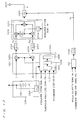
- Fig. 18 is a block diagram showing a dual-mode burst transmitter according to a seventh preferred embodiment; this dual-mode burst transmitter uses an amplitude modulation system and a constant envelope modulation system (e.g. PDC and GSM).
- the reference numeral 1807 denotes a detector circuit which converts the transmission output P into a DC voltage; part of the transmission output P is fed to a diode 1809, with the connection point between the diode 1809 and a resistor 1810 providing the output of the detector circuit 1807.
- the reference numeral 1808 denotes a detector circuit A/D converter which converts the output from the detector circuit 1807 into digital data; the output of the detector circuit A/D converter 1808 is inputted to a processor 1802 in the signal processing unit.
- the processor 1802 calculates the input-output nonlinearity of the power amplifier 2004 on the basis of the transmission power level signal PCL, the control voltage signal Vc, and the output from the detector circuit 1807, and then it sends the calculated nonlinearity information to the I/Q signal amplitude control unit 1801, while it also sends the digital control voltage data to the control voltage signal D/A converter 2006. While, in Fig.
- the function of calculating the input-output nonlinearity of the power amplifier 2004 and the function of selecting the control voltage signal are conducted in one place, these functions may be provided separately.
- the nonlinearity can be measured several times and averaged, and then the calculated result can be provided as the output.
- the I/Q signal amplitude control unit 1801 includes a waveform data generating portion 1803 and the multiplication mixers 2009.
- the waveform data generating portion 1803 of this preferred embodiment like that of the second preferred embodiment, includes a counter 1804, a table reference number generating portion 1805, and a ramp amplitude waveform data memory 1806.
- the waveform data generating portion 1803 receives as its input the nonlinearity calculated by the processor 1802, as well as the modulation system signal Sm and the transmission power level signal PCL.
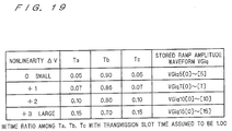
- the ramp amplitude waveform data memory 1806 stores values of the rise time Ta and the fall time Tc for the baseband signals in correspondence with the degree of nonlinearity.
- the table reference number generating portion 1805 in the waveform data generating portion 1803 therefore operates on the basis of a more variety of conditions than the table reference number generating portion 604. In other respects the configuration is the same as that shown in Fig.6 of the second preferred embodiment and therefore not described again.
- the processor 1802 outputs, to the control voltage signal D/A converter 2006, previously prepared digital control voltage data that corresponds to the target power of the transmission output P.
- the control voltage signal D/A converter 2006 then converts the digital data to an analog signal, which controls the power amplifier 2004 as the control voltage Vc.
- the digital baseband signals I and Q are ramped by using a ramp amplitude waveform Viq that corresponds to the modulation system signal Sm and the transmission power level signal PCL.
- the transmission output P is converted to a DC voltage in the detector circuit 1807, converted to digital data in the detector signal A/D converter 1808, and provided as an input to the processor 1802.
- the processor 1802 then performs feedback control to adjust the control voltage Vc to the power amplifier 2004 so as to make the detected power of the transmission output P come equal to the target power of the transmission output P; the target power of the transmission output P is thus attained finally.
- Fig. 19 shows the ratio among the rise time Ta, fall time Tc, and burst transmission section Tb of the analog baseband signals Ia and Qa with the transmission slot time assumed to be 1.00.
- ramp amplitude waveforms VPiq may be prepared considering the nonlinearity of the amplifier also in the amplitude modulation. In other respects the operation is the same as that shown in Fig. 6 of the second preferred embodiment and therefore not described again.
- the transmission output P is detected and fed back so that the nonlinearity of the power amplifier 2004 can be quantitatively grasped and the waveform of the transmission output P can be most appropriately controlled, so as to prevent the spreading of the spectrum during transmission.
- the technique of the invention can be utilized when the burst transmitter described in the first to seventh preferred embodiments is a mobile device and the modulation system is changed when it moves in a radio network from a cell in which an amplitude modulation is used into a cell in which a constant envelope modulation is used, or from a cell in which a constant envelope modulation is used into a cell in which an amplitude modulation is used.
Landscapes
- Transmitters (AREA)
- Digital Transmission Methods That Use Modulated Carrier Waves (AREA)
- Amplifiers (AREA)
Abstract
Description
- Viqup[i] :
- the ith I/Q amplitude value Viq[n] for ramp up
- Viqdown[j] :
- the jth I/Q amplitude value Viq[n] for ramp down
Where, in the expressions, "Viq" is regarded as VPiq in the case of amplitude modulation and as VGiq in the case of constant envelope modulation. - i, j :
- = 0 to 5 (in amplitude modulation)
= 0 to 7 (in constant envelope modulation) - Viq :
- I/Q maximum amplitude value
- imax :
- maximum value of i
= 5 (in amplitude modulation)
= 7 (in constant envelope modulation) - COS :
- cosine
- π :
- pi
- T :
- ramp up or ramp down time
- Δt :
- ramp voltage generation cycle time
When the baseband circuit is formed of a logic circuit, this is a discontinuous time having a certain fixed time width (Δt).
Claims (11)
- A transmission output power control device for use in a burst transmitter using a constant envelope modulation system, comprising:an I/Q signal amplitude control portion <101, 601, 1101, 1301, 1501> for variably controlling the shape of a rise and a fall of a waveform of a baseband signal and its burst transmission time from the end of the rise to the beginning of the fall;a modulator <2003> for modulating said baseband signal controlled in said I/Q signal amplitude control portion into a high-frequency signal;an amplifier <2004> for amplifying said high-frequency signal modulated in said modulator; andcontrol voltage signal selecting means for outputting a given constant voltage which is determined by a transmission power level signal, so as to control an output power of said amplifier.
- A transmission output power control device for use in a dual-mode burst transmitter using a constant envelope modulation system and an amplitude modulation system, comprising:an I/Q signal amplitude control portion <101, 601, 1101, 1301, 1501> for variably controlling the shape of a rise and a fall of a waveform of a baseband signal and its burst transmission time from the end of the rise to the beginning of the fall in accordance with a modulation system signal;a modulator <2003> for modulating the baseband signal controlled in said I/Q signal amplitude control portion into a high-frequency signal in accordance with said modulation system signal;an amplifier <2004> for amplifying said high-frequency signal modulated in said modulator; andcontrol voltage signal selecting means <102> for outputting a given constant voltage which is determined by said modulation system signal and a transmission power level signal, so as to control an output power of said amplifier.
- The transmission output power control device according to claim 1 or 2, wherein when the constant envelope modulation is used, said I/Q signal amplitude control portion variably controls the shape of the rise and the fall of the waveform of the baseband signal and the burst transmission time from the end of the rise to the beginning of the fall in accordance with said transmission power level signal.
- The transmission output power control device according to claim 1 or 2, wherein when the amplitude modulation is used, said I/Q signal amplitude control portion fixedly controls the shape of the rise and the fall of the waveform of the baseband signal and the burst transmission time from the end of the rise to the beginning of the fall, and when the constant envelope modulation is used, said I/Q signal amplitude control portion variably controls the shape of the rise and the fall of the waveform of the baseband signal and the burst transmission time from the end of the rise to the beginning of the fall in accordance with said transmission power level signal.
- The transmission output power control device according to claim 1 or 2, further comprising temperature measuring means <1106> for measuring a temperature of said amplifier, wherein said I/Q signal amplitude control portion <1101> variably controls the shape of the rise and the fall of the waveform of the baseband signal and the burst transmission time from the end of the rise to the beginning of the fall in accordance with a temperature signal obtained by said temperature measuring means.
- The transmission output power control device according to claim 1 or 2, further comprising power-supply voltage measuring means <1306> for measuring a power-supply voltage, wherein said I/Q signal amplitude control portion <1301> variably controls the shape of the rise and the fall of the waveform of the baseband signal and the burst transmission time from the end of the rise to the beginning of the fall in accordance with a power-supply voltage signal obtained by said power-supply voltage measuring means.
- The transmission output power control device according to claim 1 or 2, further comprising an electric matching adjusting circuit <1501> connected in a stage which precedes or follows said amplifier, for lessening nonlinearity of said amplifier.
- A transmission output power control device for use in a dual-mode burst transmitter using a constant envelope modulation system and an amplitude modulation system, comprising:an I/Q signal amplitude control portion <1801> for controlling the shape of a rise and a fall of a waveform of a baseband signal and its burst transmission time from the end of the rise to the beginning of the fall in accordance with a modulation system signal;a modulator <2003> for modulating said baseband signal controlled in said I/Q signal amplitude control portion into a high-frequency signal in accordance with said modulation system signal;an amplifier <2004> for amplifying said high-frequency signal modulated in said modulator;a detector <1807> for detecting an transmission output power outputted from said amplifier; anda signal processing portion <1802> for outputting a control voltage to said amplifier in accordance with a signal from said detector in such a way as to make said transmission output power attain a target output power, obtaining a difference between a target control voltage and said control voltage with which said transmission output power attained said target output power, and controlling said I/Q signal amplitude control portion so that the shape of the rise and the fall of the waveform of said baseband signal and the burst transmission time from the end of the rise to the beginning of the fall are varied in accordance with said difference.
- A transmission output power control method for use in a burst transmitter using a constant envelope modulation system, wherein the envelope of a transmission output power is controlled by variably controlling the shape of a rise and a fall of a waveform of a baseband signal and its burst transmission time from the end of the rise to the beginning of the fall.
- A transmission output power control method for use in a dual-mode burst transmitter using a constant envelope modulation system and an amplitude modulation system, wherein whichever of the modulation systems is used, the envelope of a transmission output power is controlled by variably controlling the shape of a rise and a fall of a waveform of a baseband signal and its burst transmission time from the end of the rise to the beginning of the fall.
- The transmission output power control method according to claim 10, wherein, when the amplitude modulation is used, the envelope of the transmission output power is controlled by fixedly controlling the shape of the rise and the fall of the waveform of the baseband signal and the burst transmission time from the end of the rise to the beginning of the fall, and when the constant envelope modulation is used, the envelope of the transmission output power is controlled by variably controlling the shape of the rise and the fall of the waveform of the baseband signal and the burst transmission time from the end of the rise to the beginning of the fall in accordance with a transmission power level signal.
Applications Claiming Priority (2)
| Application Number | Priority Date | Filing Date | Title |
|---|---|---|---|
| JP2001379562A JP3928421B2 (en) | 2001-12-13 | 2001-12-13 | Transmission output control apparatus and control method |
| JP2001379562 | 2001-12-13 |
Publications (2)
| Publication Number | Publication Date |
|---|---|
| EP1320191A2 true EP1320191A2 (en) | 2003-06-18 |
| EP1320191A3 EP1320191A3 (en) | 2005-01-19 |
Family
ID=19186879
Family Applications (1)
| Application Number | Title | Priority Date | Filing Date |
|---|---|---|---|
| EP02020819A Withdrawn EP1320191A3 (en) | 2001-12-13 | 2002-09-17 | Transmission output power control device for use in a burst transmitter and control method |
Country Status (4)
| Country | Link |
|---|---|
| US (1) | US6996382B2 (en) |
| EP (1) | EP1320191A3 (en) |
| JP (1) | JP3928421B2 (en) |
| CN (1) | CN1233101C (en) |
Cited By (1)
| Publication number | Priority date | Publication date | Assignee | Title |
|---|---|---|---|---|
| WO2015144701A1 (en) * | 2014-03-27 | 2015-10-01 | Telefonaktiebolaget L M Ericsson (Publ) | Radio transmitter with controllable ramp signal generation |
Families Citing this family (68)
| Publication number | Priority date | Publication date | Assignee | Title |
|---|---|---|---|---|
| US8744384B2 (en) | 2000-07-20 | 2014-06-03 | Blackberry Limited | Tunable microwave devices with auto-adjusting matching circuit |
| US8064188B2 (en) | 2000-07-20 | 2011-11-22 | Paratek Microwave, Inc. | Optimized thin film capacitors |
| JP3915811B2 (en) * | 2002-08-26 | 2007-05-16 | 三菱電機株式会社 | Waveform generation program and FM-CW radar device |
| US7123664B2 (en) * | 2002-09-17 | 2006-10-17 | Nokia Corporation | Multi-mode envelope restoration architecture for RF transmitters |
| US7373118B1 (en) * | 2003-06-27 | 2008-05-13 | Sprint Spectrum L.P. | Method and system for facilitating transmission of analog signals to a wireless terminal |
| US7010057B2 (en) * | 2003-09-04 | 2006-03-07 | Nokia Corporation | Dual mode multi-slot EGPRS transmitter |
| JP2005252471A (en) * | 2004-03-02 | 2005-09-15 | Fujitsu Ltd | Wireless communication apparatus and method for controlling amplifier circuit thereof |
| TWI244257B (en) * | 2004-06-18 | 2005-11-21 | Mediatek Inc | Control method and apparatus of transmission power amplifier |
| US7489909B2 (en) * | 2004-06-18 | 2009-02-10 | Mediatek Incorporation | Method and apparatus for controlling a TX power amplifier |
| US7327803B2 (en) | 2004-10-22 | 2008-02-05 | Parkervision, Inc. | Systems and methods for vector power amplification |
| US7355470B2 (en) | 2006-04-24 | 2008-04-08 | Parkervision, Inc. | Systems and methods of RF power transmission, modulation, and amplification, including embodiments for amplifier class transitioning |
| KR100810322B1 (en) * | 2004-10-29 | 2008-03-07 | 삼성전자주식회사 | High efficiency power amplification device and method for mobile communication |
| KR100614654B1 (en) | 2005-01-04 | 2006-08-22 | 삼성전자주식회사 | Wireless transmitters provide effective power compensation for output changes with temperature and process |
| US20130078934A1 (en) | 2011-04-08 | 2013-03-28 | Gregory Rawlins | Systems and Methods of RF Power Transmission, Modulation, and Amplification |
| US7911272B2 (en) | 2007-06-19 | 2011-03-22 | Parkervision, Inc. | Systems and methods of RF power transmission, modulation, and amplification, including blended control embodiments |
| US8013675B2 (en) | 2007-06-19 | 2011-09-06 | Parkervision, Inc. | Combiner-less multiple input single output (MISO) amplification with blended control |
| US9406444B2 (en) | 2005-11-14 | 2016-08-02 | Blackberry Limited | Thin film capacitors |
| US8325097B2 (en) | 2006-01-14 | 2012-12-04 | Research In Motion Rf, Inc. | Adaptively tunable antennas and method of operation therefore |
| US7711337B2 (en) * | 2006-01-14 | 2010-05-04 | Paratek Microwave, Inc. | Adaptive impedance matching module (AIMM) control architectures |
| US8125399B2 (en) * | 2006-01-14 | 2012-02-28 | Paratek Microwave, Inc. | Adaptively tunable antennas incorporating an external probe to monitor radiated power |
| WO2007116495A1 (en) * | 2006-03-31 | 2007-10-18 | Matsushita Electric Industrial Co., Ltd. | Transmitter apparatus and modulation scheme switching method |
| US7937106B2 (en) | 2006-04-24 | 2011-05-03 | ParkerVision, Inc, | Systems and methods of RF power transmission, modulation, and amplification, including architectural embodiments of same |
| US8031804B2 (en) | 2006-04-24 | 2011-10-04 | Parkervision, Inc. | Systems and methods of RF tower transmission, modulation, and amplification, including embodiments for compensating for waveform distortion |
| US20070270111A1 (en) * | 2006-05-19 | 2007-11-22 | Broadcom Corporation | Dual power mode transmitter |
| US7860467B2 (en) | 2006-08-29 | 2010-12-28 | Broadcom Corporation | Power control for a dual mode transmitter |
| US7714676B2 (en) | 2006-11-08 | 2010-05-11 | Paratek Microwave, Inc. | Adaptive impedance matching apparatus, system and method |
| US7535312B2 (en) | 2006-11-08 | 2009-05-19 | Paratek Microwave, Inc. | Adaptive impedance matching apparatus, system and method with improved dynamic range |
| US8299867B2 (en) | 2006-11-08 | 2012-10-30 | Research In Motion Rf, Inc. | Adaptive impedance matching module |
| US9407227B2 (en) * | 2006-11-09 | 2016-08-02 | Intel Deutschland Gmbh | Regulation of an amplification apparatus |
| WO2008074147A1 (en) * | 2006-12-21 | 2008-06-26 | Icera Canada ULC | Edge power ramp using logarithmic resistor attenuator |
| US7620129B2 (en) | 2007-01-16 | 2009-11-17 | Parkervision, Inc. | RF power transmission, modulation, and amplification, including embodiments for generating vector modulation control signals |
| US7643800B2 (en) * | 2007-01-30 | 2010-01-05 | Broadcom Corporation | Transmit power management for a communication device and method for use therewith |
| US7917104B2 (en) | 2007-04-23 | 2011-03-29 | Paratek Microwave, Inc. | Techniques for improved adaptive impedance matching |
| US8213886B2 (en) | 2007-05-07 | 2012-07-03 | Paratek Microwave, Inc. | Hybrid techniques for antenna retuning utilizing transmit and receive power information |
| WO2008144017A1 (en) | 2007-05-18 | 2008-11-27 | Parkervision, Inc. | Systems and methods of rf power transmission, modulation, and amplification |
| US8238868B2 (en) * | 2007-05-31 | 2012-08-07 | Renesas Electronics Corporation | Dynamic voltage scaling for packet-based data communication systems |
| WO2009005768A1 (en) | 2007-06-28 | 2009-01-08 | Parkervision, Inc. | Systems and methods of rf power transmission, modulation, and amplification |
| US8442456B2 (en) * | 2007-08-09 | 2013-05-14 | Freescale Semiconductor, Inc. | Wireless communication unit, integrated circuit and method of power control therein |
| US8193871B1 (en) * | 2007-10-12 | 2012-06-05 | Quintic Holdings | FM pulse shaping |
| US7991363B2 (en) | 2007-11-14 | 2011-08-02 | Paratek Microwave, Inc. | Tuning matching circuits for transmitter and receiver bands as a function of transmitter metrics |
| WO2009145887A1 (en) | 2008-05-27 | 2009-12-03 | Parkervision, Inc. | Systems and methods of rf power transmission, modulation, and amplification |
| JP5086436B2 (en) * | 2008-08-07 | 2012-11-28 | 京セラ株式会社 | Power amplifying device and transmitter and communication device using the same |
| US8072285B2 (en) | 2008-09-24 | 2011-12-06 | Paratek Microwave, Inc. | Methods for tuning an adaptive impedance matching network with a look-up table |
| US8102929B2 (en) | 2009-02-12 | 2012-01-24 | Qualcomm Incorporated | Low power ultra wideband transceiver |
| US8472888B2 (en) | 2009-08-25 | 2013-06-25 | Research In Motion Rf, Inc. | Method and apparatus for calibrating a communication device |
| US9026062B2 (en) | 2009-10-10 | 2015-05-05 | Blackberry Limited | Method and apparatus for managing operations of a communication device |
| US8803631B2 (en) | 2010-03-22 | 2014-08-12 | Blackberry Limited | Method and apparatus for adapting a variable impedance network |
| WO2011133657A2 (en) | 2010-04-20 | 2011-10-27 | Paratek Microwave, Inc. | Method and apparatus for managing interference in a communication device |
| US9379454B2 (en) | 2010-11-08 | 2016-06-28 | Blackberry Limited | Method and apparatus for tuning antennas in a communication device |
| US8712340B2 (en) | 2011-02-18 | 2014-04-29 | Blackberry Limited | Method and apparatus for radio antenna frequency tuning |
| US8655286B2 (en) | 2011-02-25 | 2014-02-18 | Blackberry Limited | Method and apparatus for tuning a communication device |
| US8626083B2 (en) | 2011-05-16 | 2014-01-07 | Blackberry Limited | Method and apparatus for tuning a communication device |
| US8594584B2 (en) | 2011-05-16 | 2013-11-26 | Blackberry Limited | Method and apparatus for tuning a communication device |
| EP2715867A4 (en) | 2011-06-02 | 2014-12-17 | Parkervision Inc | Antenna control |
| US9769826B2 (en) | 2011-08-05 | 2017-09-19 | Blackberry Limited | Method and apparatus for band tuning in a communication device |
| US8948889B2 (en) | 2012-06-01 | 2015-02-03 | Blackberry Limited | Methods and apparatus for tuning circuit components of a communication device |
| US9853363B2 (en) | 2012-07-06 | 2017-12-26 | Blackberry Limited | Methods and apparatus to control mutual coupling between antennas |
| US9246223B2 (en) | 2012-07-17 | 2016-01-26 | Blackberry Limited | Antenna tuning for multiband operation |
| US9413066B2 (en) | 2012-07-19 | 2016-08-09 | Blackberry Limited | Method and apparatus for beam forming and antenna tuning in a communication device |
| US9350405B2 (en) | 2012-07-19 | 2016-05-24 | Blackberry Limited | Method and apparatus for antenna tuning and power consumption management in a communication device |
| US9362891B2 (en) | 2012-07-26 | 2016-06-07 | Blackberry Limited | Methods and apparatus for tuning a communication device |
| US9374113B2 (en) | 2012-12-21 | 2016-06-21 | Blackberry Limited | Method and apparatus for adjusting the timing of radio antenna tuning |
| US10404295B2 (en) | 2012-12-21 | 2019-09-03 | Blackberry Limited | Method and apparatus for adjusting the timing of radio antenna tuning |
| WO2015042142A1 (en) | 2013-09-17 | 2015-03-26 | Parkervision, Inc. | Method, apparatus and system for rendering an information bearing function of time |
| JP5920853B2 (en) * | 2014-09-03 | 2016-05-18 | レノボ・イノベーションズ・リミテッド(香港) | Multi-phase DC / DC converter and control method thereof |
| US9438319B2 (en) | 2014-12-16 | 2016-09-06 | Blackberry Limited | Method and apparatus for antenna selection |
| JP2016174237A (en) * | 2015-03-16 | 2016-09-29 | 株式会社日立国際電気 | Wireless communication device |
| JP2021153248A (en) * | 2020-03-24 | 2021-09-30 | 株式会社村田製作所 | Power amplifier evaluation method and measurement system |
Family Cites Families (7)
| Publication number | Priority date | Publication date | Assignee | Title |
|---|---|---|---|---|
| US4523155A (en) * | 1983-05-04 | 1985-06-11 | Motorola, Inc. | Temperature compensated automatic output control circuitry for RF signal power amplifiers with wide dynamic range |
| FI87028C (en) | 1989-12-22 | 1992-11-10 | Nokia Mobile Phones Ltd | METHOD OF RESULT OF EFFECTIVE PROCEDURE WITHOUT SPREADING OF EFFECTIVE EFFECTS AND COVERING OF METHODS |
| FI89649C (en) | 1991-09-17 | 1993-10-25 | Nokia Mobile Phones Ltd | Procedure for increasing capacity and minimizing power consumption in a cellular radio system |
| JPH05129860A (en) | 1991-11-08 | 1993-05-25 | Oki Electric Ind Co Ltd | Power amplifier and transmitter |
| JPH0653919A (en) | 1992-07-31 | 1994-02-25 | Kyocera Corp | Automatic transmission output control device for TDMA transmitter |
| FI97179C (en) | 1994-06-15 | 1996-10-25 | Nokia Mobile Phones Ltd | Controlling the output power of a pulsed transmitter and shaping the power envelope curve |
| JPH1023089A (en) | 1996-06-28 | 1998-01-23 | Nec Corp | Transmission output control circuit |
-
2001
- 2001-12-13 JP JP2001379562A patent/JP3928421B2/en not_active Expired - Fee Related
-
2002
- 2002-07-15 US US10/194,319 patent/US6996382B2/en not_active Expired - Fee Related
- 2002-09-17 CN CN02143226.0A patent/CN1233101C/en not_active Expired - Fee Related
- 2002-09-17 EP EP02020819A patent/EP1320191A3/en not_active Withdrawn
Cited By (1)
| Publication number | Priority date | Publication date | Assignee | Title |
|---|---|---|---|---|
| WO2015144701A1 (en) * | 2014-03-27 | 2015-10-01 | Telefonaktiebolaget L M Ericsson (Publ) | Radio transmitter with controllable ramp signal generation |
Also Published As
| Publication number | Publication date |
|---|---|
| US6996382B2 (en) | 2006-02-07 |
| CN1426167A (en) | 2003-06-25 |
| JP2003179508A (en) | 2003-06-27 |
| EP1320191A3 (en) | 2005-01-19 |
| US20030114124A1 (en) | 2003-06-19 |
| JP3928421B2 (en) | 2007-06-13 |
| CN1233101C (en) | 2005-12-21 |
Similar Documents
| Publication | Publication Date | Title |
|---|---|---|
| US6996382B2 (en) | Transmission output power control device for use in a burst transmitter and control method | |
| US7443244B2 (en) | Method and apparatus for controlling a power amplifier supply voltage | |
| US20190334750A1 (en) | Symbol power tracking amplification system and a wireless communication device including the same | |
| AU620478B2 (en) | Power amplifier for a radio frequency signal | |
| CN100362745C (en) | Combined open-loop and closed-loop power control measured by using difference | |
| JP4668486B2 (en) | Method and system for adjusting maximum transmit power to maintain a constant margin for adjacent channel power rejection | |
| US5410272A (en) | RF amplifier signal-level control, and radio transmitter equipped therewith | |
| US20130187727A1 (en) | Methods for tuning an adaptive impedance matching network with a look-up table | |
| US8417199B2 (en) | Method and apparatus for improving efficiency in a power supply modulated system | |
| JP2001068940A (en) | Power amplifier circuit adjusting load of power control for adjacent channel and next to the adjacent channel | |
| US7725086B2 (en) | Method and apparatus for controlling a transmitter | |
| US20050266811A1 (en) | Ramp signal with boost portion preceding a time slot | |
| US20230085587A1 (en) | Dynamic envelope-tracking supply rail voltage setting | |
| KR101664732B1 (en) | Dynamic bias modulator with multiple output voltage converter and power amplifier using the same | |
| JP2000270032A (en) | Power control circuit and transmitter | |
| US5977833A (en) | Power supply circuit for a power amplifier of a mobile radio communication terminal | |
| US6307429B1 (en) | Extended power ramp table for power amplifier control loop | |
| US20110221417A1 (en) | Power supply apparatus and power supply control method | |
| US6983133B2 (en) | Linearization apparatus for linear automatic gain control in a mobile communication terminal and method for controlling the same | |
| JPH11251928A (en) | Automatic antenna matching circuit and method | |
| KR100603718B1 (en) | Power gain control method | |
| WO2020205398A1 (en) | Amplifier efficiency tracking in digital envelope tracking system | |
| JP2000165261A (en) | Transmission output control circuit for radio communication terminal | |
| US20090088100A1 (en) | Method and Apparatus for Regulating a Power Amplifier | |
| GB2358555A (en) | Transmitter for mobile terminal with carrier leak suppressing circuit |
Legal Events
| Date | Code | Title | Description |
|---|---|---|---|
| PUAI | Public reference made under article 153(3) epc to a published international application that has entered the european phase |
Free format text: ORIGINAL CODE: 0009012 |
|
| AK | Designated contracting states |
Designated state(s): AT BE BG CH CY CZ DE DK EE ES FI FR GB GR IE IT LI LU MC NL PT SE SK TR |
|
| AX | Request for extension of the european patent |
Extension state: AL LT LV MK RO SI |
|
| PUAL | Search report despatched |
Free format text: ORIGINAL CODE: 0009013 |
|
| AK | Designated contracting states |
Kind code of ref document: A3 Designated state(s): AT BE BG CH CY CZ DE DK EE ES FI FR GB GR IE IT LI LU MC NL PT SE SK TR |
|
| AX | Request for extension of the european patent |
Extension state: AL LT LV MK RO SI |
|
| 17P | Request for examination filed |
Effective date: 20050118 |
|
| AKX | Designation fees paid |
Designated state(s): DE FR GB |
|
| RAP1 | Party data changed (applicant data changed or rights of an application transferred) |
Owner name: MITSUBISHI DENKI KABUSHIKI KAISHA |
|
| 17Q | First examination report despatched |
Effective date: 20070906 |
|
| STAA | Information on the status of an ep patent application or granted ep patent |
Free format text: STATUS: THE APPLICATION HAS BEEN WITHDRAWN |
|
| 18W | Application withdrawn |
Effective date: 20090218 |