EP1320111A1 - Carbon nanotube contact for MEMS - Google Patents
Carbon nanotube contact for MEMS Download PDFInfo
- Publication number
- EP1320111A1 EP1320111A1 EP01811208A EP01811208A EP1320111A1 EP 1320111 A1 EP1320111 A1 EP 1320111A1 EP 01811208 A EP01811208 A EP 01811208A EP 01811208 A EP01811208 A EP 01811208A EP 1320111 A1 EP1320111 A1 EP 1320111A1
- Authority
- EP
- European Patent Office
- Prior art keywords
- contact
- nanotubes
- switch
- mwnt
- substrate
- Prior art date
- Legal status (The legal status is an assumption and is not a legal conclusion. Google has not performed a legal analysis and makes no representation as to the accuracy of the status listed.)
- Withdrawn
Links
Images
Classifications
-
- B—PERFORMING OPERATIONS; TRANSPORTING
- B82—NANOTECHNOLOGY
- B82Y—SPECIFIC USES OR APPLICATIONS OF NANOSTRUCTURES; MEASUREMENT OR ANALYSIS OF NANOSTRUCTURES; MANUFACTURE OR TREATMENT OF NANOSTRUCTURES
- B82Y10/00—Nanotechnology for information processing, storage or transmission, e.g. quantum computing or single electron logic
-
- H—ELECTRICITY
- H01—ELECTRIC ELEMENTS
- H01H—ELECTRIC SWITCHES; RELAYS; SELECTORS; EMERGENCY PROTECTIVE DEVICES
- H01H1/00—Contacts
- H01H1/0094—Switches making use of nanoelectromechanical systems [NEMS]
-
- H—ELECTRICITY
- H01—ELECTRIC ELEMENTS
- H01H—ELECTRIC SWITCHES; RELAYS; SELECTORS; EMERGENCY PROTECTIVE DEVICES
- H01H1/00—Contacts
- H01H1/06—Contacts characterised by the shape or structure of the contact-making surface, e.g. grooved
Definitions
- the invention relates to switches and relays, and a contact material therefor.
- any mechanical switch an electric circuit is closed by approaching two conductive surfaces until they touch.
- metallic contact materials are commonly used for this purpose, for example Ag, Au, Ni, Ag-SnO2, Ag-CdO2, Ni-Au for low voltage relays, Ag-W, Cu-Cr and Cu-Cr-Bi for low voltage vacuum switches and Ni-coated Cu for low voltage switches and breakers, all of which being designed for voltages of less than 1000 V.
- Ag-plated Cu or W-Cu alloys are used for high-voltage switches.
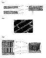
- the metal surfaces are rough on a microscopic scale. This means that when the switch is closed, most of the metal surface does not touch the opposite metal surface. The electrical contact is only established at a few contact points. This is illustrated in fig.1.
- the proposed technique relies on the use of nanotubes as the contact material for the contact surfaces.
- the effective contact area is built of a multitude of contact lines along which neighboring nanotubes belonging to different contact elements touch each other.
- the nanotubes are preferentially oriented perpendicular to the substrate, i.e. parallel to the direction of the closing or opening movement of the contact elements.
- the nanotubes are multiwalled carbon nanotubes (MWNT).
- MWNT multiwalled carbon nanotubes
- the use of carbon increases the evaporation temperature of the contact material and, due to its intrinsic resistivity, limits the amount of power supplied through a MWNT to its tip, i.e. the starting point of an arc. Hence, higher rated powers can be switched by a corresponding switch or breaker.
- Nanotube coatings can be used as a contact material.
- the concept is illustrated in fig.3.
- Two contact elements 1 with their contact surfaces 2 facing each other are part of a switch.
- a multitude of nanotubes form the contact surfaces.
- the substrate 3 may be coated with a conducting layer 4 which helps to establish a good electrical and mechanical contact to the nanotubes and comprises e.g. aluminum.
- the two contact elements 1 approach one another, the two nanotube layers penetrate each other like two brushes, thereby forming many contact lines along which two nanotube surfaces touch each other. This contrasts with the conventional contact points 5 as depicted in fig.1.
- Multiwalled carbon nanotubes can easily be grown catalytically in a dense, forest-like arrangement e.g. on top of an aluminum layer.
- Ink containing the catalyst e.g. Fe or Ni
- the sample is then exposed to a mixture of acetylene and N 2 at about 630°C.
- a dense, forest-like structure of MWNT grows perpendicular to the sample surface.
- An example is shown in fig.2, where for the purpose of visibility, a pattern of discrete MWNT-alleys has been grown. For contact applications according to the invention, the entire geometrical contact area is normally covered with MWNTs.
Landscapes
- Engineering & Computer Science (AREA)
- Chemical & Material Sciences (AREA)
- Nanotechnology (AREA)
- Physics & Mathematics (AREA)
- Mathematical Physics (AREA)
- Theoretical Computer Science (AREA)
- Crystallography & Structural Chemistry (AREA)
- Contacts (AREA)
Abstract
A low voltage switch consisting of two contact elements has a contact material forming the
contact surface and comprising nanotubes. The latter are arranged perpendicular to the
substrate and are made of carbon, i.e. multiwalled carbon nanotubes are used preferentially.
Upon closing of the switch, the nanotube layers of the two contact elements penetrate each
other like two brushes, thereby forming many contact lines as opposed to the conventional
contact points.
Description
- The invention relates to switches and relays, and a contact material therefor.
- In any mechanical switch, an electric circuit is closed by approaching two conductive surfaces until they touch. At present, preferably metallic contact materials are commonly used for this purpose, for example Ag, Au, Ni, Ag-SnO2, Ag-CdO2, Ni-Au for low voltage relays, Ag-W, Cu-Cr and Cu-Cr-Bi for low voltage vacuum switches and Ni-coated Cu for low voltage switches and breakers, all of which being designed for voltages of less than 1000 V. For high-voltage switches on the other hand, Ag-plated Cu or W-Cu alloys are used.
- In any real system, the metal surfaces are rough on a microscopic scale. This means that when the switch is closed, most of the metal surface does not touch the opposite metal surface. The electrical contact is only established at a few contact points. This is illustrated in fig.1.
- Since all the current has to pass through an effective contact area which consists of individual contact points and thus is much smaller than the macroscopic geometrical contact area, the contact resistance is much higher than what would be expected from the geometry and the conductivity of the device. A high contact resistance heats the device and contact welding is a common failure reason for existing relays and switches. In addition, a major problem of conventional devices is arcing that occurs while the switch is opened. When too much energy is deposited in the contact system, substantial damage such as destruction of the contact due to evaporation or heavy erosion might occur. This will lead to a significant limitation of the lifetime of the switch. Among the reported contact materials in vacuum arcs (Cd, Zn, Mg, Ag, Al, Cu, Cr, Ni, Fe, Ti, C, Mo, W), carbon has, together with Mo and Ti, the lowest erosion rate. Only compositions such as Ag-WC, Cu-Cr, or Cu-Cr-Bi may have even lower erosion rates. But for microswitches or MEMS (Micro Electro Mechanical System) made by silicon technology such two-component materials are hard to apply.
- It is an object of the invention to increase the effective contact area and/or to decrease the contact resistance of a switch. This object is achieved by a contact element for switches and a switch according to
claims 1 and 5. - The proposed technique relies on the use of nanotubes as the contact material for the contact surfaces. The effective contact area is built of a multitude of contact lines along which neighboring nanotubes belonging to different contact elements touch each other. The nanotubes are preferentially oriented perpendicular to the substrate, i.e. parallel to the direction of the closing or opening movement of the contact elements.
- In a preferred embodiment, the nanotubes are multiwalled carbon nanotubes (MWNT). The use of carbon increases the evaporation temperature of the contact material and, due to its intrinsic resistivity, limits the amount of power supplied through a MWNT to its tip, i.e. the starting point of an arc. Hence, higher rated powers can be switched by a corresponding switch or breaker.
- Further preferred embodiments are evident from the dependent patent claims.
- The subject matter of the invention will be explained in more detail in the following text with reference to preferred exemplary embodiments which are illustrated in the attached drawings, in which:
- Fig. 1 schematically shows a microscopic view of a state-of-the-art switch comprising two movable contact elements in an open (left) and closed (right) state,
- Fig.2 is a scanning electron micrograph of a set of catalytically grown Multiwalled Carbon Nanotubes, taken from Christian Schönenberger and Laszlo Forró, in Physics World June 2000, pp37-41, and
- Fig.3: depicts a switch according to the invention, comprising two movable contact elements in an open (left) and closed (right) state.
-
- The reference symbols used in the drawings, and their meanings, are listed in summary form in the list of reference symbols. In principle, identical parts are provided with the same reference symbols in the figures.
- Nanotube coatings can be used as a contact material. The concept is illustrated in fig.3. Two contact elements 1 with their
contact surfaces 2 facing each other are part of a switch. On asubstrate 3, a multitude of nanotubes form the contact surfaces. If required, thesubstrate 3 may be coated with a conductinglayer 4 which helps to establish a good electrical and mechanical contact to the nanotubes and comprises e.g. aluminum. When the two contact elements 1 approach one another, the two nanotube layers penetrate each other like two brushes, thereby forming many contact lines along which two nanotube surfaces touch each other. This contrasts with theconventional contact points 5 as depicted in fig.1. - Multiwalled carbon nanotubes (MWNT) can easily be grown catalytically in a dense, forest-like arrangement e.g. on top of an aluminum layer. Ink containing the catalyst (e.g. Fe or Ni) is applied to those areas where MWNT are to be grown. The sample is then exposed to a mixture of acetylene and N2 at about 630°C. At low concentrations of the catalyst in the ink, many small catalyst clusters are present and a dense, forest-like structure of MWNT grows perpendicular to the sample surface. An example is shown in fig.2, where for the purpose of visibility, a pattern of discrete MWNT-alleys has been grown. For contact applications according to the invention, the entire geometrical contact area is normally covered with MWNTs.
- There are several advantages of this method compared to the conventional contacts:
- The contact resistance is reduced, because the contact area is increased enormously. This effect is not only true for metallic nanotubes, but also compensates the higher intrinsic resistivity of inorganic and carbon MWNT compared to the conventional metallic contacts, especially because the MWNT are short (20-30µm).
- Arcing is reduced because MWNT cannot carry large currents, so that the power that is available at the possible starting point of an arc is low. Hence in this arrangement, large arcs cannot be supplied with the energy they need. Contact welding and material migration will be much less likely.
- Chemical contact contamination (e.g. oxidation) is a known problem of standard metallic relays when switching low currents. In the proposed design, this problem is also reduced because of the excellent chemical inertness of carbon nanotubes. The high chemical and mechanical stability of MWNT also highly improves the wear resistance of the contact area.
- The advantages mentioned above lead to an increased performance and lifetime of switches and relays with rated voltages of upt to 10 kV or rated currents of up to 1 kA. In particular, low-voltage switches and micro-mechanical switches incorporating a
silicon substrate 3 will benefit the most. - Preliminary results of the contact properties of two silicon substrates covered with Al and MWNT indicate that MWNT can decrease the contact resistance between macroscopic (cmscale) samples by at least one order of magnitude, compared to the case without MWNT layer.
-
- 1 Contact element
- 2 Contact surface
- 3 Substrate
- 4 Coating layer
- 5 Contact points
-
Claims (6)
- A contact element (1) for switches, with a substrate (3) and a contact surface (2) consisting of a contact material, characterized in that the contact material comprises nanotubes.
- The contact element according to claim 1, characterized in that the nanotubes are oriented at least approximately perpendicular to the substrate (3).
- The contact element according to claim 1, characterized in that the contact material comprises singlewalled or multiwalled carbon nanotubes.
- The contact element according to claim 1, characterized in that the contact material comprises inorganic nanotubes.
- A switch comprising two movable contact elements (1) according to one of claims 1 to 4.
- The switch according to claim 5, characterized in that the switch is a micro electro mechanical switch.
Priority Applications (1)
| Application Number | Priority Date | Filing Date | Title |
|---|---|---|---|
| EP01811208A EP1320111A1 (en) | 2001-12-11 | 2001-12-11 | Carbon nanotube contact for MEMS |
Applications Claiming Priority (1)
| Application Number | Priority Date | Filing Date | Title |
|---|---|---|---|
| EP01811208A EP1320111A1 (en) | 2001-12-11 | 2001-12-11 | Carbon nanotube contact for MEMS |
Publications (1)
| Publication Number | Publication Date |
|---|---|
| EP1320111A1 true EP1320111A1 (en) | 2003-06-18 |
Family
ID=8184303
Family Applications (1)
| Application Number | Title | Priority Date | Filing Date |
|---|---|---|---|
| EP01811208A Withdrawn EP1320111A1 (en) | 2001-12-11 | 2001-12-11 | Carbon nanotube contact for MEMS |
Country Status (1)
| Country | Link |
|---|---|
| EP (1) | EP1320111A1 (en) |
Cited By (7)
| Publication number | Priority date | Publication date | Assignee | Title |
|---|---|---|---|---|
| FR2853449A1 (en) * | 2003-07-17 | 2004-10-08 | Commissariat Energie Atomique | Magnetic actuator, has triggering unit that moves mobile part in manner in which contact surface of mobile part comes in electrical contact with contact surface of fixed part |
| EP1583146A3 (en) * | 2004-04-01 | 2005-10-26 | Lucent Technologies Inc. | High density nanostructured interconnection |
| WO2007118337A1 (en) * | 2006-04-13 | 2007-10-25 | Abb Research Ltd | Electrical contact assembly |
| DE102007051613A1 (en) * | 2007-10-24 | 2009-04-30 | Siemens Ag | Switching and protection device e.g. gate, for e.g. switching electric current, has current flow paths, where carbon nanotube material is aligned such that conductivity is higher in current flow direction than transverse to flow direction |
| FR2923078A1 (en) * | 2007-10-26 | 2009-05-01 | Centre Nat Rech Scient | Electrical conducting mechanical interconnection element manufacturing method for three-dimensional microelectronic device, involves carrying-out partially controlled dissolution on wires to reduce wire diameter to increase adhesion force |
| FR2930370A1 (en) * | 2008-04-18 | 2009-10-23 | Thales Sa | Electrostatic-actuation microswitch i.e. capacitor, for e.g. radar, has two armatures, of which one armature is constituted by flexible membrane with layer that is made of composite material i.e. polymer, in which nanotudes are dispersed |
| CN104576126A (en) * | 2015-01-22 | 2015-04-29 | 清华大学 | Carbon nano-tube MEMS switch and manufacturing method thereof |
Citations (2)
| Publication number | Priority date | Publication date | Assignee | Title |
|---|---|---|---|---|
| EP1087413A2 (en) * | 1999-09-24 | 2001-03-28 | Lucent Technologies Inc. | Tactile sensor comprising nanowires and method for making the same |
| EP1096523A2 (en) * | 1999-10-25 | 2001-05-02 | Lucent Technologies Inc. | Article comprising improved noble metal-based alloys and method for making the same |
-
2001
- 2001-12-11 EP EP01811208A patent/EP1320111A1/en not_active Withdrawn
Patent Citations (2)
| Publication number | Priority date | Publication date | Assignee | Title |
|---|---|---|---|---|
| EP1087413A2 (en) * | 1999-09-24 | 2001-03-28 | Lucent Technologies Inc. | Tactile sensor comprising nanowires and method for making the same |
| EP1096523A2 (en) * | 1999-10-25 | 2001-05-02 | Lucent Technologies Inc. | Article comprising improved noble metal-based alloys and method for making the same |
Cited By (14)
| Publication number | Priority date | Publication date | Assignee | Title |
|---|---|---|---|---|
| FR2853449A1 (en) * | 2003-07-17 | 2004-10-08 | Commissariat Energie Atomique | Magnetic actuator, has triggering unit that moves mobile part in manner in which contact surface of mobile part comes in electrical contact with contact surface of fixed part |
| KR101186474B1 (en) | 2004-04-01 | 2012-09-27 | 알카텔-루센트 유에스에이 인코포레이티드 | High density nanostructured interconnection |
| EP1583146A3 (en) * | 2004-04-01 | 2005-10-26 | Lucent Technologies Inc. | High density nanostructured interconnection |
| US7327037B2 (en) | 2004-04-01 | 2008-02-05 | Lucent Technologies Inc. | High density nanostructured interconnection |
| US7402913B2 (en) | 2004-04-01 | 2008-07-22 | Lucent Technologies Inc. | High density nanostructured interconnection |
| US7560817B2 (en) | 2004-04-01 | 2009-07-14 | Alcatel-Lucent Usa Inc. | Interconnect including a pliable surface and use thereof |
| CN1775656B (en) * | 2004-04-01 | 2013-06-19 | 朗迅科技公司 | Interconnection of high-density nano structure |
| WO2007118337A1 (en) * | 2006-04-13 | 2007-10-25 | Abb Research Ltd | Electrical contact assembly |
| DE102007051613A1 (en) * | 2007-10-24 | 2009-04-30 | Siemens Ag | Switching and protection device e.g. gate, for e.g. switching electric current, has current flow paths, where carbon nanotube material is aligned such that conductivity is higher in current flow direction than transverse to flow direction |
| FR2923078A1 (en) * | 2007-10-26 | 2009-05-01 | Centre Nat Rech Scient | Electrical conducting mechanical interconnection element manufacturing method for three-dimensional microelectronic device, involves carrying-out partially controlled dissolution on wires to reduce wire diameter to increase adhesion force |
| US8178416B2 (en) | 2007-10-26 | 2012-05-15 | Centre National De La Recherche Scientifique | Method for making an electrically conducting mechanical interconnection member |
| WO2009090349A3 (en) * | 2007-10-26 | 2009-09-17 | Centre National De La Recherche Scientifique | Method for making an electrically conducting mechanical interconnection member |
| FR2930370A1 (en) * | 2008-04-18 | 2009-10-23 | Thales Sa | Electrostatic-actuation microswitch i.e. capacitor, for e.g. radar, has two armatures, of which one armature is constituted by flexible membrane with layer that is made of composite material i.e. polymer, in which nanotudes are dispersed |
| CN104576126A (en) * | 2015-01-22 | 2015-04-29 | 清华大学 | Carbon nano-tube MEMS switch and manufacturing method thereof |
Similar Documents
| Publication | Publication Date | Title |
|---|---|---|
| US4570139A (en) | Thin-film magnetically operated micromechanical electric switching device | |
| Frey et al. | Metallurgical aspects of contact materials for vacuum switching devices | |
| US8183489B2 (en) | Contact element | |
| EP2006928B1 (en) | Switching element | |
| KR20010030305A (en) | Folded spring based micro electromechanical RF switch and method of making | |
| JP7221655B2 (en) | double breaker switch | |
| EP1320111A1 (en) | Carbon nanotube contact for MEMS | |
| EP4218038A1 (en) | Electric contact comprising a metal-graphene composite layer | |
| JP3054628B2 (en) | Sliding contacts for electrical equipment | |
| Cao et al. | Microrelays with bidirectional electrothermal electromagnetic actuators and liquid metal wetted contacts | |
| Sawa et al. | Recent researches and new trends of electrical contacts | |
| Oh et al. | Effects of hot switching and contamination on contact reliability of Pt-coated microswitches | |
| JPH1173848A (en) | Microswitch | |
| CN1136595C (en) | Arcing switch device | |
| Poulain et al. | A nano-scale investigation of material transfer phenomena at make in a MEMS switch | |
| WO2007118337A1 (en) | Electrical contact assembly | |
| Vincent et al. | Electrical contact reliability in a magnetic MEMS switch | |
| CN1279558C (en) | Contact structure for DC load and switchgear with the same | |
| CN1805093A (en) | sliding isolator | |
| JP4249356B2 (en) | Electrical contact material | |
| JP2000311536A (en) | Gas insulated switchgear | |
| CN215377239U (en) | Contact for a medium-voltage or high-voltage circuit breaker and medium-voltage or high-voltage circuit breaker | |
| Lindmayer et al. | The effect of unsymmetrical material combination on the contact and switching behavior | |
| CN87107122A (en) | vacuum circuit breaker | |
| Oberhammer et al. | Passive contact force and active opening force electrostatic switches for soft metal contact materials |
Legal Events
| Date | Code | Title | Description |
|---|---|---|---|
| PUAI | Public reference made under article 153(3) epc to a published international application that has entered the european phase |
Free format text: ORIGINAL CODE: 0009012 |
|
| AK | Designated contracting states |
Designated state(s): AT BE CH CY DE DK ES FI FR GB GR IE IT LI LU MC NL PT SE TR |
|
| AX | Request for extension of the european patent |
Extension state: AL LT LV MK RO SI |
|
| 17P | Request for examination filed |
Effective date: 20031120 |
|
| AKX | Designation fees paid |
Designated state(s): AT BE CH CY DE DK ES FI FR GB GR IE IT LI LU MC NL PT SE TR |
|
| 17Q | First examination report despatched |
Effective date: 20081117 |
|
| STAA | Information on the status of an ep patent application or granted ep patent |
Free format text: STATUS: THE APPLICATION IS DEEMED TO BE WITHDRAWN |
|
| 18D | Application deemed to be withdrawn |
Effective date: 20090528 |