EP1318550A2 - Semiconductor light-emitting element and optical transmission device - Google Patents
Semiconductor light-emitting element and optical transmission device Download PDFInfo
- Publication number
- EP1318550A2 EP1318550A2 EP02026252A EP02026252A EP1318550A2 EP 1318550 A2 EP1318550 A2 EP 1318550A2 EP 02026252 A EP02026252 A EP 02026252A EP 02026252 A EP02026252 A EP 02026252A EP 1318550 A2 EP1318550 A2 EP 1318550A2
- Authority
- EP
- European Patent Office
- Prior art keywords
- light
- emitting element
- semiconductor light
- wavelength
- green light
- Prior art date
- Legal status (The legal status is an assumption and is not a legal conclusion. Google has not performed a legal analysis and makes no representation as to the accuracy of the status listed.)
- Withdrawn
Links
Images


Classifications
-
- H—ELECTRICITY
- H10—SEMICONDUCTOR DEVICES; ELECTRIC SOLID-STATE DEVICES NOT OTHERWISE PROVIDED FOR
- H10H—INORGANIC LIGHT-EMITTING SEMICONDUCTOR DEVICES HAVING POTENTIAL BARRIERS
- H10H20/00—Individual inorganic light-emitting semiconductor devices having potential barriers, e.g. light-emitting diodes [LED]
- H10H20/80—Constructional details
- H10H20/84—Coatings, e.g. passivation layers or antireflective coatings
Definitions
- the present invention relates to a semiconductor light-emitting element and an optical transmission device, and in particular, to a semiconductor light-emitting element and optical transmission device which are suited to the carrying out of optical communication by use of a plastic optical fiber (hereinafter, "POF").
- PPF plastic optical fiber
- an optical transmission device which can transmit and receive light signals via a POF which is an optical transmission medium.
- the optical transmission device is equipped with a light-emitting element which emits light signals, and a light-receiving element which receives light signals from another optical transmission device.
- AlGaInP type red light-emitting diode which can respond at a high speed, is used as the light-emitting element.
- AlGaInP type red light-emitting diodes have the problems that, due to changes in temperature, the emission output decreases greatly (e.g., the emission output decreases to about 60% with respect to a change in temperature of 100°C) and the emission wavelength also varies greatly (e.g., the emission wavelength varies by about 20 nm with respect to a change in temperature of 100°C).
- the transmission loss at the POF there are great variations in the transmission loss at the POF, and the transmission distance is limited to about 50 m.
- GaN type green light-emitting diodes (wavelength: 520 nm), which emit green light which is in a wavelength region in which the loss of the POF is low, have come onto the market as displays.
- a GaN type green light-emitting diode can emit green light which is in a wavelength region in which the loss of the POF is low.
- a GaN type green light-emitting diode has the advantages that, as compared with a red light-emitting diode, there is little decrease in the emission output with respect to changes in temperature (e.g., the emission output decreases to about 75% with respect to a change in temperature of 100°C), and there is also little variation in the emission wavelength with respect to changes in temperature (e.g., the emission wavelength varies by about 3.3 nm with respect to a change in temperature of 100°C).
- the emission wavelength varies by about 3.3 nm with respect to a change in temperature of 100°C.
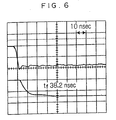
- Fig. 6 is a diagram showing the measured waveform at the falling time of a GaN type green light-emitting diode.
- the upper line which has been drawn is the driving current waveform of a GaN type green light-emitting diode
- the lower line which has been drawn is the emission output waveform.
- the falling characteristic of the light output during digital operation of the GaN type green light-emitting diode i.e., the time t f required for the output to change from 90% to 10%
- the time t f required for the output to change from 90% to 10% is about 38 nsec.
- a GaN type green light-emitting diode can only output light signals to about 20 Mbps, and cannot be used as a device for high-speed optical communication.
- the present invention has been proposed in order to overcome the above-described drawbacks, and an object of the present invention is to provide a semiconductor light-emitting element and an optical transmission device whose response characteristics are improved by the falling time of a light signal outputted from a GaN type green light-emitting diode being shortened.
- the present invention overcomes the above-described drawbacks by utilizing the property that the long-wavelength components of green light emitted by a GaN type green light-emitting diode slow the falling time of the emission output.
- a first aspect of the present invention is a semiconductor light-emitting element comprising: a GaN type green light-emitting diode emitting green light; and a wavelength selecting element selecting and outputting only light of wavelengths at which a falling time of emission output of the GaN type green light-emitting diode is less than or equal to an average value.
- a semiconductor light-emitting element comprising: a GaN type green light-emitting diode emitting green light; and a wavelength selecting element selecting and outputting only light of wavelengths at which a falling time of emission output of the GaN type green light-emitting diode is less than or equal to an average value.
- the wavelength selecting element it is possible for the wavelength selecting element to select and output only light of wavelengths of 520 nm or less from the green light. Because the wavelength of the green light outputted from the wavelength selecting element becomes 520 nm or less, the falling time can be shortened to 50 nsec or less, and the response speed can be improved.
- the wavelength selecting element select and output only light of wavelengths of less than or equal to a central wavelength of an emission spectrum of the green light.
- the central wavelength of the emission spectrum of the green light is about 515 nm.
- the wavelength selecting element selects and outputs light whose wavelength is 515 nm or less from the green light emitted from the GaN type green light-emitting diode. In this way, because the falling time can be shortened to about 40 nsec or less, the response speed can be improved even more.
- a second aspect of the present invention is an optical transmission device comprising: a semiconductor light-emitting element having a GaN type green light-emitting diode emitting green light, and a wavelength selecting element selecting and outputting only light of wavelengths at which a falling time of emission output of the GaN type green light-emitting diode is less than or equal to an average value; and an optical fiber transmitting the green light emitted by the semiconductor light-emitting element.
- optical communication can be carried out by using green light having an improved response speed.
- the loss of the light signal at the optical fiber can be suppressed, and decreases in output due to fluctuations in temperature can be reduced.
- long distance transmission which was impossible with conventional red light-emitting diodes, can be carried out.
- a third aspect of the present invention is an optical transmission device comprising: a first GaN type green light-emitting diode emitting green light; a light-receiving element receiving green light from a second GaN type green light-emitting diode which is different from the first GaN type green light-emitting diode; and a wavelength selecting element provided at at least one of a light-emitting surface of the first GaN type green light-emitting diode and a light-receiving surface of the light-receiving element, and selecting and outputting only light of wavelengths at which a falling time of emission output of one of the first and second GaN type green light-emitting diodes is less than or equal to an average value.
- the wavelength selecting element select and output, from the green light, only light of wavelengths of 520 nm or less, or only light of wavelengths less than or equal to the central wavelength of the emission spectrum of the green light.
- Fig. 1 is a diagram showing the response characteristic (a rising time t r [msec], a falling time t f [msec], and an output amplitude [mV], with respect to respective wavelengths) when respective wavelengths are separated from the emission wavelength of a GaN type green light-emitting diode (hereinafter called "GaN type green LED"). Note that spectra of 0.6 nm were obtained by a spectroscope along the full width at half maximum for the respective wavelengths in the emission spectrum of the GaN type green LED.
- the output amplitude values have the same configuration as the emission spectrum of the GaN type green LED.
- the falling time t f became longer in proportion to the wavelength. This means that the falling characteristic deteriorates due to the light components at the longer wavelength side of the central wavelength of the emission spectrum.
- the falling time t f is a minimum of 20 nsec at the short wavelength side, and is a maximum of 80 nsec at the long wavelength side.
- the falling time t f can be shortened, and the response speed can be improved.
- Fig. 2 is a diagram showing the schematic structure of an optical transmission device 1 relating to an embodiment of the present invention.
- the optical transmission device 1 transmits and receives light signals via a POF 2 which is an optical transmission medium.
- the optical transmission device 1 includes a semiconductor light-emitting element 10 which emits green light, an LED driving circuit 20 which drives the semiconductor light-emitting element 10, and a light-receiving element 30 which receives green light via the POF 2 from another optical transmission device.
- Fig. 3 is a diagram showing the structure of the semiconductor light-emitting element 10.
- the semiconductor light-emitting element 10 has a GaN type green LED 11 which emits green light, and a wavelength selecting element 12 which selects and outputs only predetermined wavelength components.
- the GaN type green LED 11 emits green light having output amplitudes [mV] of the same configuration as the emission spectrum.
- the central wavelength of the green light is about 515 nm.
- the wavelength selecting element 12 is formed by an interference filter or an etalon, and selects and outputs only wavelength components of 520 nm or less from the green light from the GaN type green LED 11. In this way, the falling time t f of the green light outputted from the wavelength selecting element 12 is 50 nsec or less.
- the wavelength 520 nm is a wavelength which is slightly longer than the central wavelength of the emission spectrum. Thus, at the wavelength 520 nm, some wavelength components which slow down the response speed are included in the output amplitude.
- a wavelength selecting element 12 which selects and outputs wavelengths at the shorter wavelength side of the central wavelength (i.e., wavelengths of 515 nm or less), may be used.
- Fig. 4 is a diagram showing another structure of the semiconductor light-emitting element 10.
- a multilayer filter 13 is formed at the light-emitting surface side of the GaN type green LED 11 of the semiconductor light-emitting element 10, i.e., on the GaN end surface.
- the multilayer filter 13 selects and outputs only wavelengths of 520 nm or less from the green light from the GaN type green LED 11. In this way, the falling time t f of the green light outputted from the multilayer filter 13 is 50 nsec or less. If it is desired to make the response speed even faster, a multilayer filter, which selects and outputs only wavelengths at the shorter wavelength side of the central wavelength (i.e., wavelengths of 515 nm or less), may be used.
- the configuration of the electrode of the GaN type green LED 11 is not particularly limited. However, in order for the green light to efficiently optically couple with the POF 2, the following configuration may be used for example.
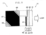
- Fig. 5 is a diagram showing the structure of the GaN type green LED 11.
- Fig. 5 includes a plan view showing the GaN type green LED 11 as viewed from the electrode side and a cross-sectional view of the GaN type green LED 11.
- n-GaN layer 42 of a thickness of 2 ⁇ m, an n-Al 0.1 Ga 0.9 N layer 43 of a thickness of 0.1 ⁇ m, an InGaN/GaN multi-quantum well 44, a p-Al 0.1 Ga 0.9 N layer 45 of a thickness of 0.1 ⁇ m, and a p-GaN layer 46 are formed in that order on one surface of a transparent sapphire substrate 41.
- a positive electrode 47 is formed on the p-GaN layer 46. Note that a portion of the n-GaN layer 42 is exposed to the exterior. A negative electrode 48 is formed at the exposed portion of the n-GaN layer 42.
- the positive electrode 47 is rectangular as shown in Fig. 5. Note that the configurations of the positive electrode 47 and the negative electrode 48 are not limited to those shown in Fig. 5, and may be other configurations.
- the GaN type green LED 11 which is structured in this way outputs green light corresponding to the configurations of the positive electrode 47 and the negative electrode 48.
- the green light outputted from the GaN type green LED 11 can be efficiently optically coupled with the POF 2.
- a light-emitting element which can operate at high speed can be realized by outputting only the short wavelengths among the green light emitted at the GaN type green LED 11.
- the optical transmission device 1 which is equipped with the semiconductor light-emitting element 10 transmits a light signal which uses only short wavelengths of the green light emitted at the GaN type green LED 11.
- the falling time t f of the light signal can be shortened, and therefore, the response speed can be improved.
- the optical transmission device 1 can achieve a response speed which is equivalent to or better than that of conventional red LEDs, light signals of wavelengths at which there is low loss at the POF 2 can be outputted without resulting in high costs. Moreover, even if fluctuations in temperature arise, a decrease in the emission output and fluctuations in the wavelength can be suppressed as compared with the case of using a red LED. As a result, an optical datalink system enabling transmission of 100 m or more, which could not be achieved with conventional red LEDs, can be realized at a low cost.
- the wavelength selecting element 12 is provided at the semiconductor light-emitting element 10.
- the wavelength selecting element 12 may be provided at the light-receiving element 30.
- an interference filter or etalon may provided as the wavelength selecting element 12, or a multilayer filter may be provided.
- the optical transmission device 1 can improve the response speed of the transmitted light signal.
Landscapes
- Led Devices (AREA)
- Optical Communication System (AREA)
- Semiconductor Lasers (AREA)
Abstract
Description
Claims (10)
- A semiconductor light-emitting element (10), comprising
a GaN type green light-emitting diode (11) emitting green light, and
a wavelength selecting element (12, 13) selecting and outputting only light of wavelengths at which a falling time of emission output of the GaN type green light-emitting diode is less than or equal to an average value. - The semiconductor light-emitting element of claim 1, wherein the wavelength selecting element (12, 13) selects and outputs only light of wavelengths of 520 nm or less from the green light.
- The semiconductor light-emitting element of claim 1 or 2, wherein the wavelength selecting element (12, 13) selects and outputs only light of wavelengths of 515 nm or less from the green light.
- The semiconductor light-emitting element of one of claims 1 to 3, wherein the wavelength selecting element (12, 13) selects and outputs only light of wavelengths less than or equal to a central wavelength of an emission spectrum of the green light.
- The semiconductor light-emitting element of one of claims 1 to 4, wherein the wavelength selecting element (12, 13) is adhered to a light-emitting surface of the GaN type green light-emitting diode (11).
- The semiconductor light-emitting element of one of claims 1 to 5, wherein the wavelength selecting element comprises a multilayer filter (13), and/or an interference filter (12), and/or an etalon (12).
- An optical transmission device, comprising
a semiconductor light-emitting element (10) according to one of claims 1 to 6, and
an optical fiber (2) transmitting the green light emitted by the semiconductor light-emitting element. - The optical transmission device of claim 7, wherein an electrode of the semiconductor light-emitting element (10) is formed in a configuration corresponding to a cross-sectional configuration of the optical fiber (2).
- The optical transmission device of claim 8, wherein the electrode of the semiconductor light-emitting element is formed to be circular.
- An optical transmission device, comprising
a first semiconductor light-emitting element (10), and
a light-receiving element (30) receiving green light from a second semiconductor light-emitting element which is different from the first semiconductor light-emitting element (10),
wherein the first and/or the second semiconductor light-emitting element(s) is/are a semiconductor light-emitting element according to one of claims 1 to 6.
Applications Claiming Priority (2)
| Application Number | Priority Date | Filing Date | Title |
|---|---|---|---|
| JP2001361191 | 2001-11-27 | ||
| JP2001361191A JP2003163369A (en) | 2001-11-27 | 2001-11-27 | Semiconductor light emitting device and optical transmission device |
Publications (2)
| Publication Number | Publication Date |
|---|---|
| EP1318550A2 true EP1318550A2 (en) | 2003-06-11 |
| EP1318550A3 EP1318550A3 (en) | 2004-01-07 |
Family
ID=19171892
Family Applications (1)
| Application Number | Title | Priority Date | Filing Date |
|---|---|---|---|
| EP02026252A Withdrawn EP1318550A3 (en) | 2001-11-27 | 2002-11-26 | Semiconductor light-emitting element and optical transmission device |
Country Status (3)
| Country | Link |
|---|---|
| US (1) | US20030099445A1 (en) |
| EP (1) | EP1318550A3 (en) |
| JP (1) | JP2003163369A (en) |
Families Citing this family (2)
| Publication number | Priority date | Publication date | Assignee | Title |
|---|---|---|---|---|
| JP2007287851A (en) * | 2006-04-14 | 2007-11-01 | Toyoda Gosei Co Ltd | LIGHT EMITTING ELEMENT USED FOR OPTICAL COMMUNICATION AND COMMUNICATION DEVICE USING THE SAME |
| JP5428714B2 (en) * | 2009-09-30 | 2014-02-26 | 住友電気工業株式会社 | Optical communication device and optical transmitter |
Family Cites Families (14)
| Publication number | Priority date | Publication date | Assignee | Title |
|---|---|---|---|---|
| GB1377936A (en) * | 1972-09-20 | 1974-12-18 | Us Envelope Co | Rotary cutting apparatus |
| JPS58149837U (en) * | 1982-03-31 | 1983-10-07 | オムロン株式会社 | light level converter |
| JPH01262684A (en) * | 1988-04-13 | 1989-10-19 | Fujitsu Ltd | Device and method for emitting pulsed light |
| JP2656837B2 (en) * | 1989-11-13 | 1997-09-24 | 日本電信電話株式会社 | Optical pulse generation method, generator and transmission method |
| JPH06310805A (en) * | 1993-04-20 | 1994-11-04 | Teratetsuku:Kk | Short pulse light generation set |
| DE69433694T2 (en) * | 1993-11-02 | 2004-08-12 | Matsushita Electric Industrial Co., Ltd., Kadoma | Semiconductor component with an aggregate of micro-needles made of semiconductor material |
| JPH08250767A (en) * | 1995-03-13 | 1996-09-27 | Nichia Chem Ind Ltd | Nitride semiconductor LED |
| JPH08307018A (en) * | 1995-05-11 | 1996-11-22 | Nippon Telegr & Teleph Corp <Ntt> | Optical signal generator |
| JP3729001B2 (en) * | 1996-12-27 | 2005-12-21 | 日亜化学工業株式会社 | Light emitting device, bullet-type light emitting diode, chip type LED |
| JPH10200154A (en) * | 1997-01-10 | 1998-07-31 | Toshiba Corp | Optical semiconductor device and method of manufacturing the same |
| JP3966954B2 (en) * | 1997-09-01 | 2007-08-29 | 東芝電子エンジニアリング株式会社 | Illumination device, reading device, projection device, purification device, and display device |
| US6233265B1 (en) * | 1998-07-31 | 2001-05-15 | Xerox Corporation | AlGaInN LED and laser diode structures for pure blue or green emission |
| US7039322B1 (en) * | 1998-12-24 | 2006-05-02 | Mitsubishi Rayon Co., Ltd. | Optical communication apparatus |
| JP2001160631A (en) * | 1999-12-01 | 2001-06-12 | Citizen Electronics Co Ltd | Structure of surface mount infrared communication module |
-
2001
- 2001-11-27 JP JP2001361191A patent/JP2003163369A/en active Pending
-
2002
- 2002-11-26 EP EP02026252A patent/EP1318550A3/en not_active Withdrawn
- 2002-11-26 US US10/303,820 patent/US20030099445A1/en not_active Abandoned
Also Published As
| Publication number | Publication date |
|---|---|
| JP2003163369A (en) | 2003-06-06 |
| EP1318550A3 (en) | 2004-01-07 |
| US20030099445A1 (en) | 2003-05-29 |
Similar Documents
| Publication | Publication Date | Title |
|---|---|---|
| US6794688B2 (en) | Semiconductor light-emitting device and manufacturing method therefor, and LED lamp and LED display | |
| Lee et al. | 26 Gbit/s LiFi system with laser-based white light transmitter | |
| JP4464888B2 (en) | Optical communication transmitter, optical communication receiver, optical communication system, and communication apparatus | |
| US6229834B1 (en) | Led display device | |
| US9447933B2 (en) | Visible light communication system | |
| JP2007095844A (en) | Semiconductor light emitting composite device | |
| WO2010044129A1 (en) | Semiconductor light-emitting element array and manufacturing method thereof | |
| US12184329B2 (en) | Wavelength-division multiplexing visible-light communication and lighting device and method | |
| JP2008311532A (en) | White light emitting device and method for forming white light emitting device | |
| KR101558241B1 (en) | Fabricating method of light emitting device | |
| KR20110053228A (en) | Light emitting element | |
| WO2017060836A1 (en) | An apparatus comprising a waveguide-modulator and laser-diode and a method of manufacture thereof | |
| KR101848804B1 (en) | Optical module, optical transceiver and communication system including the same | |
| US8417072B2 (en) | Light emitting device and optical transmission system | |
| KR102050407B1 (en) | Vertically stacked multi-wavelength light emitting device | |
| US20200259314A1 (en) | Systems including vertical cavity surface emitting lasers | |
| CN118215867A (en) | Optical fiber links based on visible wavelength LEDs | |
| US20030099445A1 (en) | Semiconductor light-emitting element and optical transmission device | |
| KR100550846B1 (en) | Gallium nitride based light emitting diode with flip chip bonding structure | |
| US7342364B2 (en) | Light source | |
| JPH0818097A (en) | Light emitting diode | |
| JPH09318853A (en) | Optical transceiver and optical communication network | |
| JPH08130508A (en) | Optical transmission system, bidirectional optical transmission system, optical multiplex transmission system, spatial optical transmission system, and spatial optical multiplex transmission system | |
| US6961033B2 (en) | GaN green LED drive device and optical transmission device | |
| JP2000174398A (en) | Semiconductor light emitting device, pointing device and optical transmission device |
Legal Events
| Date | Code | Title | Description |
|---|---|---|---|
| PUAI | Public reference made under article 153(3) epc to a published international application that has entered the european phase |
Free format text: ORIGINAL CODE: 0009012 |
|
| 17P | Request for examination filed |
Effective date: 20021126 |
|
| AK | Designated contracting states |
Designated state(s): AT BE BG CH CY CZ DE DK EE ES FI FR GB GR IE IT LI LU MC NL PT SE SK TR |
|
| AX | Request for extension of the european patent |
Extension state: AL LT LV MK RO SI |
|
| PUAL | Search report despatched |
Free format text: ORIGINAL CODE: 0009013 |
|
| AK | Designated contracting states |
Kind code of ref document: A3 Designated state(s): AT BE BG CH CY CZ DE DK EE ES FI FR GB GR IE IT LI LU MC NL PT SE SK TR |
|
| AX | Request for extension of the european patent |
Extension state: AL LT LV MK RO SI |
|
| AKX | Designation fees paid |
Designated state(s): DE FR GB |
|
| 17Q | First examination report despatched |
Effective date: 20040419 |
|
| STAA | Information on the status of an ep patent application or granted ep patent |
Free format text: STATUS: THE APPLICATION IS DEEMED TO BE WITHDRAWN |
|
| 18D | Application deemed to be withdrawn |
Effective date: 20051116 |