EP1317089A2 - Attenuation devices - Google Patents
Attenuation devices Download PDFInfo
- Publication number
- EP1317089A2 EP1317089A2 EP02257841A EP02257841A EP1317089A2 EP 1317089 A2 EP1317089 A2 EP 1317089A2 EP 02257841 A EP02257841 A EP 02257841A EP 02257841 A EP02257841 A EP 02257841A EP 1317089 A2 EP1317089 A2 EP 1317089A2
- Authority
- EP
- European Patent Office
- Prior art keywords
- optical
- stream
- demux
- mux
- output
- Prior art date
- Legal status (The legal status is an assumption and is not a legal conclusion. Google has not performed a legal analysis and makes no representation as to the accuracy of the status listed.)
- Withdrawn
Links
Images




Classifications
-
- H—ELECTRICITY
- H04—ELECTRIC COMMUNICATION TECHNIQUE
- H04B—TRANSMISSION
- H04B10/00—Transmission systems employing electromagnetic waves other than radio-waves, e.g. infrared, visible or ultraviolet light, or employing corpuscular radiation, e.g. quantum communication
- H04B10/25—Arrangements specific to fibre transmission
- H04B10/2507—Arrangements specific to fibre transmission for the reduction or elimination of distortion or dispersion
- H04B10/25073—Arrangements specific to fibre transmission for the reduction or elimination of distortion or dispersion using spectral equalisation, e.g. spectral filtering
-
- G—PHYSICS
- G02—OPTICS
- G02B—OPTICAL ELEMENTS, SYSTEMS OR APPARATUS
- G02B6/00—Light guides; Structural details of arrangements comprising light guides and other optical elements, e.g. couplings
- G02B6/24—Coupling light guides
- G02B6/26—Optical coupling means
- G02B6/264—Optical coupling means with optical elements between opposed fibre ends which perform a function other than beam splitting
- G02B6/266—Optical coupling means with optical elements between opposed fibre ends which perform a function other than beam splitting the optical element being an attenuator
-
- G—PHYSICS
- G02—OPTICS
- G02B—OPTICAL ELEMENTS, SYSTEMS OR APPARATUS
- G02B6/00—Light guides; Structural details of arrangements comprising light guides and other optical elements, e.g. couplings
- G02B6/10—Light guides; Structural details of arrangements comprising light guides and other optical elements, e.g. couplings of the optical waveguide type
- G02B6/12—Light guides; Structural details of arrangements comprising light guides and other optical elements, e.g. couplings of the optical waveguide type of the integrated circuit kind
- G02B6/12007—Light guides; Structural details of arrangements comprising light guides and other optical elements, e.g. couplings of the optical waveguide type of the integrated circuit kind forming wavelength selective elements, e.g. multiplexer, demultiplexer
- G02B6/12009—Light guides; Structural details of arrangements comprising light guides and other optical elements, e.g. couplings of the optical waveguide type of the integrated circuit kind forming wavelength selective elements, e.g. multiplexer, demultiplexer comprising arrayed waveguide grating [AWG] devices, i.e. with a phased array of waveguides
- G02B6/12019—Light guides; Structural details of arrangements comprising light guides and other optical elements, e.g. couplings of the optical waveguide type of the integrated circuit kind forming wavelength selective elements, e.g. multiplexer, demultiplexer comprising arrayed waveguide grating [AWG] devices, i.e. with a phased array of waveguides characterised by the optical interconnection to or from the AWG devices, e.g. integration or coupling with lasers or photodiodes
- G02B6/12021—Comprising cascaded AWG devices; AWG multipass configuration; Plural AWG devices integrated on a single chip
-
- H—ELECTRICITY
- H04—ELECTRIC COMMUNICATION TECHNIQUE
- H04B—TRANSMISSION
- H04B2210/00—Indexing scheme relating to optical transmission systems
- H04B2210/25—Distortion or dispersion compensation
- H04B2210/258—Distortion or dispersion compensation treating each wavelength or wavelength band separately
Definitions
- the invention relates to optical attenuation devices, in particular to such devices for attenuating the individual signals in a multiplexed optical stream.
- the invention also relates to methods of attenuating a multiplexed optical stream.
- optical signals are transported by optical fibres.
- signals are transported as multiplexed streams, typically in dense wavelength division multiplexed format; the transport bandwidth of the fibre is divided into a number, typically forty, of evenly spaced wavelength or colour channels, and signals on each channel are combined into a multiplexed stream.
- Optical signals in optical communications networks require amplification periodically to offset losses incurred in transportation.
- One method of amplification is with optical fibre amplifiers such as erbium doped fibre amplifiers (EDFAs).
- An EDFA may comprise a length of erbium doped active optical fibre; the input signal for amplification is transported along the active fibre that is also pumped with light which raises energy levels. The input signal stimulates downward transitions resulting in photons at the wavelength of the input signal, thereby amplifying it.
- a fibre amplifier will be located at a node in the network along with various other devices which may carry out required processes on incoming multiplexed streams.
- fibre amplifiers tend to have a non-uniform gain profile; that is to say, gain may vary across the operable wavelength band of the amplifier. This equates to differences in amplification between the signals on successive channels in a multiplexed stream. In addition, changes in the gain profile may result from differences in power between the signals on successive channels. It is desirable to be able to tailor the gain profile to specific requirements rather than to have to make do with the gain profile of the fibre amplifier. In one specific instance, "flat gain" across the transport bandwidth is required.
- a device which enables the degree of attenuation on each channel within a spectrum to be continually varied may be referred to as a dynamic gain flattening filter (DGFF).
- DGFF dynamic gain flattening filter
- Such individual channel attenuation may be achieved by including a thermo optical attenuator on each of the output channels of a de-multiplexer and a static reflector at the de-multiplexed output plane, or the channels from the output plane may continue and be re-multiplexed.
- a DGFF with thermo optical attenuators requires a large number of heaters (one for each channel) and can lead to thermal effects on the de-multiplexer.
- thermo optical attenuators have the downsides of polarisation dependence, high thermal load, high electrical dissipation.
- An object of the invention is to provide an attenuation device with the facility to dynamically attenuate each channel in a multiplexed optical stream. Moreover, it is an object to provide such a device with high resolution, low optical loss and simple construction.
- the invention provides an optical attenuation device comprising an input/output on which a multiplexed optical input stream is received, a multiplexer/de-multiplexer (MUX/DEMUX) for separating the received stream into individual optical signals on individual channels, an output/return path from the MUX/DEMUX for each of the channels, reflector means in each output/return path for reflecting all or a proportion of the optical signal on the respective channel back along the output/return path to the MUX/DEMUX, wherein the optical signals are recombined by the MUX/DEMUX into a multiplexed stream which is output on the input/output.
- MUX/DEMUX multiplexer/de-multiplexer
- At least one of the reflector means may be a MEMS actuated mirror.
- Each mirror may be displaced longitudinally, transversely or angularly thereby to control the proportion of individual optical signal reflected.
- An angularly displaced mirror is preferred because it is relatively insensitive to polarisation requirements and relatively small movements of the mirror are all that is needed to achieve the necessary attenuation of, say, 10-20dB.
- the optical signal beams may be of the order of 10 ⁇ m in diameter, and movements of 100-200 ⁇ m may be needed to achieve the necessary attenuation.
- a transversely displaced mirror may be hampered by polarisation dependence.
- MEMS actuated mirrors are electrostatically actuated, which involves low net electrical dissipation.
- MEMS actuated or any other mirrors may be fabricated using semi-conductor material substrates.
- each reflector means may be a MARS-type device including two mirrors arranged generally parallel to one another thereby to define a cavity with the relative spacing of the mirrors variable so as to control the proportion of optical signal reflected according to interference effects.
- each reflector means may be a mirror in combination with a controllable, optically absorbing material; the material may be placed to the signal side of the mirror and controlled so as to limit the proportion of the signal getting to and from the mirror.
- the MUX/DEMUX may be a planar waveguide device, which may be fabricated from semi-conductor material substrates.
- the optical attenuation device may further comprise a circulator or an entity of an equivalent function which enables the output multiplexed stream to be diverted on to a different branch from the input multiplexed stream.
- the invention provides an optical attenuation device for attenuating a multiplexed optical stream comprising means for attenuating each of the individual optical signals of the stream in parallel.
- the loss associated with each channel is independent of the loss of any other channel.
- the invention provides an optical attenuation device comprising an input on which a multiplexed optical input stream is received, a first MUX/DEMUX separating the received stream into individual optical signals on individual channels, an output path from the MUX/DEMUX for each of the channels, attenuator means in each output path attenuating the optical signal on the respective channel, a return path from the attenuator means for each of the channels, a second MUX/DEMUX at the ends of the return paths, and an output from the second MUX/DEMUX, wherein the attenuated optical signals are combined at the second MUX/DEMUX into a multiplexed stream which is output on the output.
- the attenuator means may be a reflector means such that attenuation is achieved by reflecting all or a proportion of the optical signal on the respective channel. Any of the reflector means discussed with reference to the first aspect of the invention may be appropriate.
- the attenuator means may be a transmission means such that attenuation is achieved by transmitting all or a proportion of the optical signal on the respective channel.
- the transmissions means may comprise a shutter, possibly a MEMS actuated shutter, which is controllably positioned so as to limit the proportion of the optical signal passing.
- the shutter is so designed as to be polarisation independent.
- the invention provides a method of attenuating a multiplexed optical stream comprising de-multiplexing the stream thereby to separate the stream into individual optical signals, attenuating at least one of the signals by reflection and multiplexing the attenuated signals thereby to combine the signals into a multiplexed stream.
- the attenuation of at least one of the signals may be achieved by reflecting all or a proportion of the signal or by transmitting all or a proportion of the signal.
- the invention provides a method of attenuating a multiplexed optical stream comprising the de-multiplexing the stream thereby to separate the stream into individual optical signals attenuating each signal in parallel with the other signals and mutiplexing the attenuated signals thereby to combine the signals into a multiplexed optical stream.
- the invention provides reflector means for an optical attenuation device according to a first or third aspects of the invention.
- the invention provides MUX/DEMUX for an optical attenuation device according to a first, second or third aspects of the invention.
- the invention provides a node in an optical communications network incorporating at least one attenuation device according to a first, second or third aspects of the invention.
- the transport bandwidth of an optical fibre (not shown) is divided into twenty-one individual, evenly spaced wavelength channels; on each channel there is an individual optical signal.
- the individual signals have been combined into a multiplexed optical stream.
- the multiplexed stream has been amplified at an Erbium doped fibre amplifier (EDFA) and, because of the non-uniform gain profile of the EDFA, the spectrum of the multiplexed stream has a non-uniform profile, with each of the channels amplified to a different extent.
- EDFA Erbium doped fibre amplifier
- the multiplexed stream requires dynamic attenuation, that is, with each of the individual optical signals attenuated to a greater or lesser degree so as to effect a flat gain profile.
- Such dynamic attenuation is achieved by utilising an attenuation device according to the invention.
- an attenuation device comprises a multiplexer/de-multiplexer (MUX/DEMUX) 2 and a dynamic mirror array 4 having n mirrors.
- the device is located at a node (not shown) in a optical communications network.
- a multiplexed optical stream is received on the input/output 6 to the MUX/DEMUX 2.
- the stream is received from an EDFA 8 via a circulator 10 on branch 16.
- the multiplexed stream is separated by the MUX/DEMUX 2 into its individual channels. Between the MUX/DEMUX 2 and the array 4 there is an output/return path 12 for each of the channels.
- Each path 12 terminates at one mirror 4 1 ,4 2 ,....4 n in the mirror array 4.
- An individual signal arriving at the corresponding mirror 4 x along a path 12 x is reflected back along the path 12 x to the MUX/DEMUX 2.
- the proportion of signal which is reflected is controlled by varying the displacement of the mirror 4 x .
- the reflected individual signals are re-combined to form an attenuated multiplexed optical stream which is output on the input/output 6 to the circulator 10 and out along branch 18.
- the non-uniform effects of the EDFA 8 can be smoothed so that the output multiplexed stream has a flat gain profile.
- the attenuation of a signal on one channel may occur simultaneously with the attenuation of one or more other signals on one or more other channels.
- the mirrors 4 x may operate in parallel and the individual signals may be attenuated in parallel.
- a specific embodiment of the invention uses a planar waveguide MUX/DEMUX 202 to separate an incoming multiplexed optical stream into individual optical signals.
- Planar waveguide multiplexer/de-multiplexers are well known, but briefly they achieve separation and recombination by utilising interference effect generated as a result of transporting signals along parallel, different length waveguide paths.
- the output/return paths 212 from the MUX/DEMUX 202 are also planar waveguides. Reflection back to the MUX/DEMUX is achieved by means of a MEMS mirror array 204 with a linear array of mirrors 204 1 , 204 2 ...204 n each individually electrostatically actuable.
- the planar waveguide MUX/DEMUX 202 is fabricated from semiconductor material substrates and joined to form hybrid working parts with the MEMS mirror array 204 located such that each mirror 204 x is aligned with one output/return path 212. Between the end of the output/return path 212 and the respective mirror 204 x , the individual signal propagates as a free space beam of the order of 10 ⁇ m in diameter.
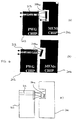
- each mirror 204 x can be used to control a degree of reflection: either (a) the mirror 204 x can be moved longitudinally, that is, back and forth in relation to the axis of the output/return path 212 and, because the beam is a free space beam between the waveguide 212 and the mirror 204 x , so as to utilise the inevitable dispersion of the beam on its path to and from the mirror 204 x such that only a proportion of the reflected signal is captured back in the waveguide 212; (b) the mirror 204 x may be pivoted so as to direct a proportion of the reflected beam "off axis" so that it is not captured by the waveguide 212; (c) the mirror 204 x may move transversely, that is, perpendicularly to the axis of the waveguide 212, so that only the proportion of the beam which is cut by the mirror 204 x
- a so-called MARS-type mirror device indicated generally at 601 which has two co-axial but spaced apart partial mirrors 602, 604 defining a tunable mirror cavity 605 with the distance between the mirrors 602, 604 variable thereby to change the degree of reflection according to the resulting interference effects.
- an attenuation device comprises a first MUX/DEMUX 2, a dynamic shutter array 40 having n shutters and a second MUX/DEMUX 20.
- the device is located at a node (not shown) in an optical communications network.
- a multiplexed optical stream is received on the input/output 6 to the MUX/DEMUX 2.
- the multiplexed stream is separated by the MUX/DEMUX 2 into its individual channels.
- the array 40 there is an output path 12 for each of the channels.
- Each path 12 terminates at one shutter 40 1 , 40 2 ........ 40 n in the shutter array 40.
- Each path 120 commences from one of the shutters 40 1 , 40 2 ........40 n in the shutter array 40.
- An individual signal arriving at the corresponding shutter 40 x along an output path 12 x is attenuated by the shutter and the attenuated signal passes along the output path 120 x to the second MUX/DEMUX 20.
- the degree of attenuation is controlled by the position of the shutter 40 x .
- At the second MUX/DEMUX 20 attenuated individual signals are recombined to form an attenuated multiplexed optical stream which is output on an output 60.
- line G represents the non-linear gain profile of an EDFA operating in the so-called C band of wavelengths, with a wavelength channel spacing of 2nm
- line E represents the profile following dynamic attenuation across all of the channels using the device described with reference to figure 2.
- an optical attenuation device has an input/output 6 on which a multiplexed optical input stream is received.
- a multiplexer/de-multiplexer (MUX/DEMUX) 2 separates the received stream into individual optical signals on individual channels and has an output/return path 12 from the MUX/DEMUX 2 for each of the channels.
- Reflector means 4 in each output/return path 12 reflects all or a proportion of the optical signal on the respective channel back along the output/return path 12 to the MUX/DEMUX 2.
- the optical signals are combined into a multiplexed stream which is output on the input/output 6.
- the device has first and second MUX/DEMUX 2, 20, an output path 12 from the first MUX/DEMUX 2, attenuation means 40 at the end of each output path 12 and return paths 120 from the attenuation means 40 to the second MUX/DEMUX 20.
- the attenuation means attenuates the optical signals on the respective channels, and the attenuated signals are combined into a multiplexed stream at the second MUX/DEMUX 20. Both embodiments achieve attenuation of multiplexed optical streams by attenuating the component optical signals of the stream in parallel.
Landscapes
- Physics & Mathematics (AREA)
- General Physics & Mathematics (AREA)
- Optics & Photonics (AREA)
- Spectroscopy & Molecular Physics (AREA)
- Electromagnetism (AREA)
- Engineering & Computer Science (AREA)
- Computer Networks & Wireless Communication (AREA)
- Signal Processing (AREA)
- Optical Communication System (AREA)
Abstract
Description
Claims (19)
- An optical attenuation device comprising an input/output (6) on which a multiplexed optical input stream is received, a multiplexer/de-multiplexer (MUX/DEMUX) (2) for separating the received stream into individual optical signals on individual channels, an output/return path from the MUX/DEMUX for each of the channels, reflector means (4) in each output/return path (12) for reflecting all or a proportion of the optical signal on the respective channel back along the output/return path to the MUX/DEMUX, wherein the optical signals are re-combined by the MUX/DEMUX into a multiplexed stream which is output on the input/output.
- An optical attenuation device according to claim 1 wherein at least one reflector means comprises a MEMS actuated mirror.
- An optical attenuation device according to claim 2 wherein the or each mirror is displaced longitudinally, transversely or angularly thereby to control the proportion of individual optical signal reflected.
- An optical attenuation device according to claim 2 or claim 3 wherein the or each mirror is electrostatically actuated.
- An optical attenuation device according to any of claims 2-4 wherein the or each mirror is fabricated using semi-conductor material substrates.
- An optical attenuation device according to claim 1 wherein at least one reflector means comprises a MARS-type device (601) including two mirrors (602, 604) arranged generally parallel to one another thereby to define a cavity (605) with the relative spacing of the mirrors variable so as to control the proportion of optical signal reflected according to interference effects.
- An optical attenuation device according to claim 1 wherein at least one reflector reflector means comprises a mirror in combination with a controllable, optically absorbing material.
- An optical attenuation device according to any of the preceding claims wherein the MUX/DEMUX is a planar waveguide device.
- An optical attenuation device according to any of the preceding claims wherein the MUX/DEMUX is which may be fabricated from semi-conductor material substrates.
- An optical attenuation device according to any of the preceding claims further comprising a circulator or an entity of an equivalent function which enables the output multiplexed stream to be diverted on to a different branch from the input multiplexed stream.
- An optical attenuation device for attenuating a multiplexed optical stream comprising means for attenuating each of the individual optical signals of the stream in parallel.
- An optical attenuation device comprising an input (6) on which a multiplexed optical input stream is received, a first MUX/DEMUX (2) separating the received stream into individual optical signals on individual channels, an output path (12) from the MUX/DEMUX for each of the channels, attenuator means (40) in each output path attenuating the optical signal on the respective channel, a return path (120) from the attenuator means for each of the channels, a second MUX/DEMUX (20) at the ends of the return paths, and an output (60) from the second MUX/DEMUX, wherein the attenuated optical signals are combined at the second MUX/DEMUX into a multiplexed stream which is output on the output.
- An optical attenuation device according to claim 12 wherein the attenuator means comprises reflector means such that attenuation is achieved by reflecting all or a proportion of the optical signal on the respective channel.
- An optical attenuation device according to claim 12 wherein the attenuator means comprises transmission means such that attenuation is achieved by transmitting all or a proportion of the optical signal on the respective channel.
- A method of attenuating a multiplexed optical stream comprising de-multiplexing the stream thereby to separate the stream into individual optical signals, attenuating at least one of the signals by reflection and multiplexing the attenuated signals thereby to combine the signals into a multiplexed stream.
- A method of attenuating a multiplexed optical stream comprising the de-multiplexing the stream thereby to separate the stream into individual optical signals attenuating each signal in parallel with the other signals and mutiplexing the attenuated signals thereby to combine the signals into a multiplexed optical stream.
- Reflector means for an optical attenuation device according to claim 1 or claim 13.
- MUX/DEMUX for an optical attenuation device according to claim 1 or claim 12.
- An optical communications network incorporating at least one optical attenuation device according to claim 1, claim 11 or claim 12.
Applications Claiming Priority (2)
| Application Number | Priority Date | Filing Date | Title |
|---|---|---|---|
| US992619 | 1992-12-18 | ||
| US09/992,619 US6862395B2 (en) | 2001-11-16 | 2001-11-16 | Attenuation devices |
Publications (2)
| Publication Number | Publication Date |
|---|---|
| EP1317089A2 true EP1317089A2 (en) | 2003-06-04 |
| EP1317089A3 EP1317089A3 (en) | 2005-04-06 |
Family
ID=25538543
Family Applications (1)
| Application Number | Title | Priority Date | Filing Date |
|---|---|---|---|
| EP02257841A Withdrawn EP1317089A3 (en) | 2001-11-16 | 2002-11-13 | Attenuation devices |
Country Status (3)
| Country | Link |
|---|---|
| US (1) | US6862395B2 (en) |
| EP (1) | EP1317089A3 (en) |
| CA (1) | CA2412040C (en) |
Families Citing this family (6)
| Publication number | Priority date | Publication date | Assignee | Title |
|---|---|---|---|---|
| US20030161574A1 (en) * | 2002-02-22 | 2003-08-28 | Aksyuk Vladimir Anatolyevich | Planar lightwave wavelength device using moveable mirrors |
| US7149378B2 (en) | 2002-02-22 | 2006-12-12 | Lucent Technologies Inc. | Monolithic waveguide/MEMS switch |
| TWI229051B (en) * | 2002-08-23 | 2005-03-11 | Asia Pacific Microsystems Inc | Movable inclined reflector based signal processing device and its method |
| US6993219B2 (en) * | 2003-03-13 | 2006-01-31 | Lucent Technologies Inc. | Waveguide/MEMS switch |
| FR2863125B1 (en) * | 2003-12-02 | 2006-12-29 | Cit Alcatel | RECONFIGURABLE OPTICAL DEVICE WITH CONTROLLED INSERTION / EXTRACTION (S) |
| US9362708B2 (en) * | 2013-09-20 | 2016-06-07 | Alcatel Lucent | Compact two-stage optical amplifier |
Family Cites Families (10)
| Publication number | Priority date | Publication date | Assignee | Title |
|---|---|---|---|---|
| JPH0596825U (en) * | 1991-09-25 | 1993-12-27 | スタンレー電気株式会社 | Reflector |
| US5519796A (en) * | 1995-03-06 | 1996-05-21 | International Business Machines Corporation | Gain equalization using monolithic planar waveguide grating multiplexer and demultiplexer |
| JPH10173597A (en) * | 1996-12-06 | 1998-06-26 | Nec Corp | Optical equalizer |
| US5949571A (en) * | 1998-07-30 | 1999-09-07 | Lucent Technologies | Mars optical modulators |
| US5943155A (en) * | 1998-08-12 | 1999-08-24 | Lucent Techonolgies Inc. | Mars optical modulators |
| US6148124A (en) * | 1998-11-20 | 2000-11-14 | Lucent Technologies | Wavelength division multiplexed optical networks |
| JP2000174699A (en) * | 1998-12-02 | 2000-06-23 | Nec Corp | Optical demultiplexing / multiplexing circuit for wavelength division multiplexing transmission |
| GB2363014B (en) * | 1999-06-30 | 2002-02-13 | Marconi Comm Ltd | Optical System |
| US6636657B1 (en) * | 1999-07-07 | 2003-10-21 | Lucent Technolgies Inc. | Channelized wavelength division multiplex equalizer using reflective attenuators |
| US6556338B2 (en) * | 2000-11-03 | 2003-04-29 | Intpax, Inc. | MEMS based variable optical attenuator (MBVOA) |
-
2001
- 2001-11-16 US US09/992,619 patent/US6862395B2/en not_active Expired - Fee Related
-
2002
- 2002-11-13 EP EP02257841A patent/EP1317089A3/en not_active Withdrawn
- 2002-11-15 CA CA2412040A patent/CA2412040C/en not_active Expired - Fee Related
Also Published As
| Publication number | Publication date |
|---|---|
| CA2412040C (en) | 2014-10-07 |
| EP1317089A3 (en) | 2005-04-06 |
| CA2412040A1 (en) | 2003-05-16 |
| US6862395B2 (en) | 2005-03-01 |
| US20030095777A1 (en) | 2003-05-22 |
Similar Documents
| Publication | Publication Date | Title |
|---|---|---|
| KR100705865B1 (en) | Apparatus, systems and methods comprising an optical integrated circuit having an integrated array waveguide grating and an optical amplifier | |
| CA2014552C (en) | Optical repeater and optical network using the same | |
| US6104527A (en) | High efficiency bandwidth doubled and gain flattened silica fiber amplifier | |
| US6304370B1 (en) | Two-stage modular wide-band optical amplifiers | |
| US8204379B2 (en) | Noise reduction in optical communications networks | |
| JPH10173597A (en) | Optical equalizer | |
| KR100334432B1 (en) | Bidirectional add / drop optical amplifier module using one waveguide thermal lattice multiplexer | |
| US5140655A (en) | Optical star coupler utilizing fiber amplifier technology | |
| US6222962B1 (en) | Optical amplifier | |
| US20020126372A1 (en) | Optical signal repeating and amplifying device and optical level adjusting device | |
| US6456428B1 (en) | Optical amplifier | |
| US6862395B2 (en) | Attenuation devices | |
| KR100649903B1 (en) | Optical transmission system and optical amplifying apparatus, optical amplifying unit, and optical coupler for the same | |
| KR100342516B1 (en) | Band-split bidirectional add/drop multiplexer and amplifier module with common mid-stage devices | |
| CN1430347A (en) | Optical relay amplifier and wave division multiplexer | |
| US6917467B2 (en) | Optical amplifier | |
| US7019893B2 (en) | Optical dynamic gain amplifier | |
| KR100342427B1 (en) | Multi-stage bidirectional optical amplifier | |
| US20030184847A1 (en) | Optical multiplexers and demultiplexers | |
| EP1006688A2 (en) | Optical multiplexer/demultiplexer circuit for wavelenght division multiplex transmission | |
| US6577416B1 (en) | Channel control in a wavelength division multiplexed communications network | |
| US6643059B1 (en) | Optical array amplifier | |
| JP4520700B2 (en) | Signal addition for wavelength division multiplexing systems. | |
| KR20030075657A (en) | Gain-providing optical power equalizer | |
| KR100600626B1 (en) | Improved bidirectional optical amplifier structure |
Legal Events
| Date | Code | Title | Description |
|---|---|---|---|
| PUAI | Public reference made under article 153(3) epc to a published international application that has entered the european phase |
Free format text: ORIGINAL CODE: 0009012 |
|
| AK | Designated contracting states |
Designated state(s): AT BE BG CH CY CZ DE DK EE ES FI FR GB GR IE IT LI LU MC NL PT SE SK TR |
|
| AX | Request for extension of the european patent |
Extension state: AL LT LV MK RO SI |
|
| PUAL | Search report despatched |
Free format text: ORIGINAL CODE: 0009013 |
|
| AK | Designated contracting states |
Kind code of ref document: A3 Designated state(s): AT BE BG CH CY CZ DE DK EE ES FI FR GB GR IE IT LI LU MC NL PT SE SK TR |
|
| AX | Request for extension of the european patent |
Extension state: AL LT LV MK RO SI |
|
| 17P | Request for examination filed |
Effective date: 20051006 |
|
| AKX | Designation fees paid |
Designated state(s): DE FR GB |
|
| 17Q | First examination report despatched |
Effective date: 20051115 |
|
| STAA | Information on the status of an ep patent application or granted ep patent |
Free format text: STATUS: THE APPLICATION IS DEEMED TO BE WITHDRAWN |
|
| 18D | Application deemed to be withdrawn |
Effective date: 20070406 |