EP1317085A2 - A method and circuit for initializing a de-skewing buffer in a clock forwarded system - Google Patents
A method and circuit for initializing a de-skewing buffer in a clock forwarded system Download PDFInfo
- Publication number
- EP1317085A2 EP1317085A2 EP02026822A EP02026822A EP1317085A2 EP 1317085 A2 EP1317085 A2 EP 1317085A2 EP 02026822 A EP02026822 A EP 02026822A EP 02026822 A EP02026822 A EP 02026822A EP 1317085 A2 EP1317085 A2 EP 1317085A2
- Authority
- EP
- European Patent Office
- Prior art keywords
- circuit
- buffer
- pointer
- data
- clock
- Prior art date
- Legal status (The legal status is an assumption and is not a legal conclusion. Google has not performed a legal analysis and makes no representation as to the accuracy of the status listed.)
- Granted
Links
Images


Classifications
-
- G—PHYSICS
- G06—COMPUTING OR CALCULATING; COUNTING
- G06F—ELECTRIC DIGITAL DATA PROCESSING
- G06F5/00—Methods or arrangements for data conversion without changing the order or content of the data handled
- G06F5/06—Methods or arrangements for data conversion without changing the order or content of the data handled for changing the speed of data flow, i.e. speed regularising or timing, e.g. delay lines, FIFO buffers; over- or underrun control therefor
- G06F5/10—Methods or arrangements for data conversion without changing the order or content of the data handled for changing the speed of data flow, i.e. speed regularising or timing, e.g. delay lines, FIFO buffers; over- or underrun control therefor having a sequence of storage locations each being individually accessible for both enqueue and dequeue operations, e.g. using random access memory
-
- H—ELECTRICITY
- H04—ELECTRIC COMMUNICATION TECHNIQUE
- H04L—TRANSMISSION OF DIGITAL INFORMATION, e.g. TELEGRAPHIC COMMUNICATION
- H04L7/00—Arrangements for synchronising receiver with transmitter
-
- H—ELECTRICITY
- H04—ELECTRIC COMMUNICATION TECHNIQUE
- H04L—TRANSMISSION OF DIGITAL INFORMATION, e.g. TELEGRAPHIC COMMUNICATION
- H04L7/00—Arrangements for synchronising receiver with transmitter
- H04L7/0016—Arrangements for synchronising receiver with transmitter correction of synchronization errors
- H04L7/005—Correction by an elastic buffer
-
- G—PHYSICS
- G06—COMPUTING OR CALCULATING; COUNTING
- G06F—ELECTRIC DIGITAL DATA PROCESSING
- G06F2205/00—Indexing scheme relating to group G06F5/00; Methods or arrangements for data conversion without changing the order or content of the data handled
- G06F2205/10—Indexing scheme relating to groups G06F5/10 - G06F5/14
- G06F2205/104—Delay lines
-
- H—ELECTRICITY
- H04—ELECTRIC COMMUNICATION TECHNIQUE
- H04L—TRANSMISSION OF DIGITAL INFORMATION, e.g. TELEGRAPHIC COMMUNICATION
- H04L7/00—Arrangements for synchronising receiver with transmitter
- H04L7/0008—Synchronisation information channels, e.g. clock distribution lines
-
- H—ELECTRICITY
- H04—ELECTRIC COMMUNICATION TECHNIQUE
- H04L—TRANSMISSION OF DIGITAL INFORMATION, e.g. TELEGRAPHIC COMMUNICATION
- H04L7/00—Arrangements for synchronising receiver with transmitter
- H04L7/04—Speed or phase control by synchronisation signals
- H04L7/10—Arrangements for initial synchronisation
Definitions
- This invention relates to clock forwarded communication systems.
- a clock forwarded interface is becoming more common in systems for communication between various devices within the system. Clock forwarded interfaces may typically offer higher speed, higher bandwidth communication among the devices as compared to traditional bus architectures.
- a clock forwarded interface generally includes point-to-point transfers of data between a sender and a receiver.
- the sender provides a clock, referred to as a forward clock, to the receiver that causes the receiver to capture the transmitted data.
- the sender synchronizes the transmitted data to the forwarded clock.
- the receiver may capture the data responsive to the forward clock and then synchronize the data to its own internal clock.
- the clock provided by the sender and the receiver clock are typically derived from the same external clock source. Therefore, both clocks are frequency matched. However, due to such factors as internal component gate delays and clock trace length mismatches, the forwarded clock and the internal receiver clock may be out of phase with each other. This is referred to as static phase mismatch. Other factors, such a temperature variations, may cause the phase relationship to change during operation. This is referred to as dynamic phase mismatch. Since the phase relationship between the two clocks is unknown, the data is typically buffered at the receiving device using a first-in, first-out (FIFO) buffer.
- the FIFO buffer typically uses a write pointer and a read pointer which are clocked by the forward clock and the internal clock, respectively.
- Data received on the clock-forwarded interface is written into the FIFO buffer using the write pointer and read from the FIFO buffer using the read pointer.
- the possibility of data corruption exists by reading data from the FIFO buffer before that data is stable from the write.
- a method and circuit for initializing a buffer in a clock forwarded system is provided.
- the buffer is configured for temporarily storing incoming data received on the clock-forwarded interface.
- the buffer may use a write pointer and a read pointer which may be clocked by two different clocks allowing independent write and read accesses to the buffer.
- a predetermined pattern of data may be written into an entry in the buffer.
- a logic circuit may detect the predetermined pattern of data and may cause the value of the write pointer to be captured.
- a synchronizing circuit may synchronize an indication that the predetermined pattern of data has been detected to the clock used by the read pointer.
- the synchronizer circuit may then provide an initialize signal to the read pointer which stores the captured write pointer value into the read pointer.
- This captured write pointer value becomes the initial value of the read pointer, effectively offsetting the read pointer from the write pointer.
- This separation of the write and read pointers may account for the static phase mismatch between the two clocks. Additional delay may be optionally added to the synchronizer circuit to provide margin for the dynamic phase mismatch.
- a circuit comprising a buffer for storing data, wherein the buffer includes a plurality of entries; a write pointer coupled to the buffer, a read pointer coupled to the buffer, a first circuit, and a synchronizing circuit.
- the write pointer is configured to sequentially indicate each one of the plurality of entries in the buffer into which data is to be written, and is clocked by a first clock.
- the read pointer is configured to sequentially indicate each one of said plurality of entries in the buffer from which data is to be read, and is clocked by a second clock.
- the first circuit is configured to generate a pointer value in response to an indication that a predetermined pattern of data is transmitted to the buffer for storage.
- the first circuit is coupled to the read pointer.
- the synchronizing circuit is coupled to the read pointer and to receive the indication, and is configured to generate a signal to the read pointer responsive to the indication.
- the read pointer is configured to update to the pointer value from the first circuit responsive to the signal.
- a method of initializing a buffer is contemplated.
- a predetermined pattern of data transmitted for storage in one of a plurality of entries in the buffer responsive to a first clock is detected.
- a pointer value is generated in response to the detecting.
- An indication of the detecting is synchronized to a second clock.
- a read pointer is updated to the pointer value responsive to the synchronizing.
- a send unit 10 transmits data to a receive unit 50 through a first connection INData 80.
- INData is at least one bit wide and may be any desired number of bits wide.
- Send unit 10 also transmits a clock signal TCLK 90 to receive unit 50.
- send unit 10 and receive unit 50 may include any devices (e.g. processors, peripheral devices, etc.).
- the transmitted data is synchronous to TCLK 90 such that in this example the data on INData 80 may be captured by a receive buffer circuit 100 on the rising edge of TCLK 90. It is noted however, that in other embodiments the falling edge of TCLK 90 or both edges of TCLK 90 may be used.
- TCLK 90 (and RCLK 70) will be used as the data reference, but as noted, the falling edge or both edges may be used in other contemplated embodiments.
- Data is written into receive buffer circuit 100 using TCLK 90 and read out of receive buffer 60 using a second clock signal RCLK 70, which is local to receive unit 50.
- RCLK 70 and TCLK 90 are frequency matched, but may not be phase matched. More particularly, RCLK 70 and TCLK 90 are sourced from the same clock source (CLK source 40 in FIG. 1). Both RCLK 70 and TCLK 90 may be generated from input clock signals from CLK source 40 (circuitry not shown).
- receive buffer circuit 100 may be configured with independent write and read pointers allowing independent write and read accesses.
- the read pointer is offset from the write pointer using an initialization procedure.
- a block diagram of one embodiment of the receive buffer circuit 100 is shown.
- a buffer 105 is coupled to a write pointer 130 and a read pointer 120, and is further coupled to receive the input data (INData 80) and to provide output data (data out 170).
- a flop 112 is coupled to the write pointer 130 and the read pointer 120.
- the flop 112 is further coupled to an AND gate 113, which is coupled to receive an inversion of the TCLK 90 (through an inverter 135) and an output of an initialization detection logic circuit 114 (referred to below as "logic circuit 114").
- the logic circuit 114 is coupled to a flop 117 which is coupled to receive the INData 80 and to a flop 115, which is further coupled to a synchronizer 145 and an N delay circuit 160.
- the N delay circuit 160 is further coupled to provide an init signal 161 to the read pointer 120.
- the logic circuit 114 is further coupled to receive in init trigger signal 109.
- the write pointer 130 and the flop 117 and flop 115 are clocked by the TCLK 90, while the synchronizer 145, the N delay circuit 160, and the read pointer 120 are clocked by the RCLK 70.
- Buffer 105 may include a plurality of entries, each of which are capable of storing a data transfer from INData 80. In other words, each entry is capable of storing the number of bits transferred on INData 80 in response to one edge of TCLK 90.
- the entries of buffer 105 are addressed by write pointer 130 and read pointer 120.
- Write pointer 130 may include a counter circuit which is clocked by TCLK 90 and may run continuously. In this particular embodiment, the counter circuit is an up counter and is incremented for each data transfer (modulo the number of entries in buffer 105). However, it is contemplated that, in other embodiments, the counter may be a down counter that is decremented for each data transfer (modulo the number of entries in buffer 105).
- Write pointer 130 points to the entry in buffer 105 that data arriving on INData 80 will be written to responsive to the next rising edge of TCLK 90. Therefore, upon transfer of data synchronized to TCLK 90, data is written into a buffer 105 entry indicated by the value in the write pointer and the write pointer is incremented to address the next entry.
- Read pointer 120 To read data out of buffer 105 (e.g. via a data out port 170), read pointer 120 is used. Read pointer 120 points to the entry in buffer 105 from which data will be read responsive to RCLK 70. Generally, data is read as frequently as it is written (e.g. on the rising edge, falling edge or both). Read pointer 120 may include a counter circuit which is clocked by RCLK 70 and may run continuously. It is noted that in this particular embodiment the counter circuit is an up counter, but it is contemplated that in other embodiments the counter circuit may be a down counter. Data is read out of an entry in buffer 105 indicated by the value in the read pointer and the read pointer is incremented to address the next entry responsive to RCLK 70.
- read pointer 120 is initialized with separation from write pointer 130. This initialization process is described next. After a system reset or other circuit main reset, receive buffer circuit 100 is initialized. A predetermined initialization value may be written into each entry in buffer 105, if desired, although other embodiments may not initialize the buffer entries. In this example, the predetermined initialization value may be all zeros. However, it is noted that the value may be any value. The initialization values are written for a number of cycles at least equal to the number of entries in buffer 105. The initialization values may be written for a number of clock cycles greater than the number of entries in buffer 105, as desired. A predetermined pattern of data is written to at least one entry in buffer 105.
- the predetermined pattern of data is all ones. However, it is noted that the predetermined pattern of data may be any pattern that is different from the initialization value (if initialization is used). It is contemplated that the initializing data and the predetermined pattern of data may be transmitted by send unit 10 of FIG. 1. Alternatively, one or both of the initializing data and the predetermined pattern of data may come from a pattern generation circuit local to receive unit 50 (not shown).
- logic circuit 114 When in initialization mode, logic circuit 114 is configured to detect reception of the predetermined pattern of data.
- the flop 117 captures data from INData 80 in response to the TCLK 90.
- the logic circuit 114 decodes the data to detect the predetermined pattern of data, and outputs a signal to the flop 115 and to the AND gate 113 indicating whether or not the pattern has been detected.
- the AND gate 113 in response to the TCLK signal being low (the inverted TCLK signal being high) and the output of the logic circuit 114 being high, causes the flop 112 to capture the value of the write pointer 130.
- the flop 112 provides the captured value to the read pointer 120.
- the counter circuit of read pointer 120 is set to the captured value in response to an activated init signal 161 from the synchronizing circuit 140 (described in more detail below).
- Init trigger 109 activates the initialization mode, and may be activated in response to any initialization event (e.g. system reset).
- any initialization event e.g. system reset.
- logic circuit 114 may not assert its output signal, thus preventing reinitializing the read pointer 120 during ordinary operating mode.
- the logic circuit 114 may assert the output signal in response to the first detection of the predetermined pattern of data and then may inhibit assertion of the output signal thereafter during initialization mode in order to capture the write pointer at the first detection of the predetermined pattern.
- the synchronizing circuit 140 samples the output signal of the logic circuit 114 according to the TCLK 90 in the flop 115. Generally, and described in greater detail below, synchronizing circuit 140 synchronizes the output signal to the local clock domain of RCLK 70 (using the synchronizer 145). As described above, the synchronizer circuit 140 provides init signal 161 to read pointer 120 responsive to the output signal from the logic circuit 114. Specifically, once the synchronizer 145 synchronizes the output signal, the synchronizing circuit 140 may output the init signal 161. In the illustrated embodiment, an optional N delay circuit 160 is included and adds N clock cycles of delay to the output signal before asserting the init signal 161. It is noted that the delay (the "N”) may be a static value, or may be configurable (e.g. the number of flops used may be programmable) and may be selected according to the conditions in a given system.
- the synchronizer 145 may, for example, include two flip-flops connected serially and clocked by RCLK 70.
- the data input to the synchronizer may be the output of the flop 115.
- Other embodiments may use more or less flip-flops.
- On the first rising edge of RCLK 70 after the data appears at the input to the first flip-flop the data is clocked to the output of the first flip-flop, which is the input to the second flip-flop.
- the data On the next rising edge of RCLK 70, the data is clocked to the output of the second flip-flop. In this way, the data is synchronized to RCLK 70.
- the output of synchronizer 145 is coupled to the input of the optional N delay circuit 160.
- the N delay circuit 160 delays the synchronized data by N cycles.
- the N cycle delay provides an additional separation between the read pointer 120 and the write pointer 130. The additional separation may allow a margin for dynamic phase mismatch between TCLK 90 and RCLK 70.
- the N delay circuit 160 may comprise a series connection of N flops clocked by the RCLK 70. In the example illustrated in Figs. 3A-3B below, N delay circuit 160 delays the synchronized data by one cycle and N delay circuit 160 includes one flip-flop that is clocked by RCLK 70. In other embodiments, N delay circuit 160 may delay the synchronized data by more or fewer cycles, and may contain more or fewer flip-flops. It is also contemplated that N delay circuit 160 may include other circuit components that achieve the same delay response as the present embodiment.
- N delay circuit 160 The output of N delay circuit 160 is init signal 161, which is provided to read pointer 120.
- read pointer 120 updates its counter value to the captured write pointer value provided by flop 112.
- Write pointer 130 continues to run, responsive to TCLK 90, as the predetermined data pattern is detected and synchronized to RCLK 70. Thus, when read pointer 120 is updated to the captured write pointer value, there is separation between the read pointer 120 and the write pointer 130.
- the logic circuit 114 is shown in Fig. 2, other embodiments may eliminate the logic circuit 114 and the flop 115.
- the predetermined pattern of data may be one bit of the data on INData 80 (or, in the case of a predetermined pattern of all ones or all zeros, one bit may be sufficient to detect the pattern).
- the flop 117 may capture the bit of the INData 80 as the pattern detection signal.
- a second logic circuit is coupled to the buffer 105.
- the second logic circuit detects which of the entries of the buffer 105 is updated with the predetermined pattern of data and generates a pointer value indicative of that entry.
- the second logic circuit may replace the flop 112 and the AND gate 113.
- flop circuits 112, 115, and 117 are shown in Fig. 2 (and are described as part of an example of the synchronizer 145 and the N delay circuit 160), any clocked storage device may be used in other embodiments (e.g. flops, registers, latches, etc.).
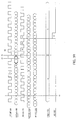
- FIG. 3A an exemplary timing diagram of one embodiment of receive buffer circuit 100 of FIG. 2 is shown.
- the timing diagram of FIG. 3A in conjunction with circuit elements of FIG. 2, illustrates the relationships between the TCLK signal and its corresponding data and write pointer and the RCLK signal and its corresponding read pointer.
- the abbreviation RPTR is used for read pointer 120
- the abbreviation WPTR is used for write pointer 130.
- INData is synchronized to TCLK such that ideally the transferring edge of TCLK would be placed in the center of any data window (e.g. the rising edge in the illustrated embodiment or, in embodiments in which the falling edge or both edges are used, the falling edge or the falling and rising edges).
- a receiving device such as, for example, buffer 105 of FIG. 2 may capture the data on that transmitting edge. It is noted however, that the data may not be centered around the rising edge of TCLK and may in fact be skewed to the left or right within some specified limits.
- RCLK is frequency matched to TCLK but not in phase with TCLK. As shown in the example of FIG. 3A, the rising edge of RCLK occurs before the rising edge of TCLK. This example depicts one way that TCLK and RCLK may be out of phase with each other. Referring back to timing reference t0, the write counter value WPTR and the read counter value both start at zero, although any random values could occur in various embodiments. At the rising edge of each clock, the respective counter values increment to the next value.
- Initialization data is written into buffer 105 of FIG. 2 for at least enough cycles to ensure that buffer 105 is initialized.
- the data on INData 80 is all zeros for each data transfer.
- each entry of buffer 105 is initialized to all zeros.
- the WPTR 130 reaches seven (assuming buffer 105 has eight entries for this example), it rolls over to zero again.
- the data changes to all ones (the predetermined pattern of data for this example). While the data changes to the predetermined pattern of data when WPTR 130 is at entry zero in this example, the predetermined pattern may be transmitted when WPTR 130 is at any entry.
- TCLK timing reference t1
- the logic circuit 114 of FIG. 2 detects the predetermined pattern of data in the flop 117 and asserts its output signal.
- TCLK timing reference t3
- the flop 112 captures the value of the write pointer 130 (the value is 1 in this example).
- the logic circuit 114 may operate within 1/2 TCLK cycle.
- flop 115 captures the asserted output signal.
- the first flip-flop of synchronizer 145 captures the asserted signal.
- N delay circuit 160 of FIG. 2 captures the data.
- the output of the N delay circuit 160 is the init signal pulse on init signal 161 (labeled 'd' in Fig. 3A). This pulse causes RPTR 120 to update to the value from flop 112 (i.e. one in this example).
- FIG. 3B a timing diagram of one embodiment of receive buffer circuit 100 of FIG. 2 is shown. Similar to the description of FIG. 3A, the timing diagram of FIG. 3B also illustrates the relationships between the TCLK signal and its corresponding data and write pointer and the RCLK signal and its corresponding read pointer. However, in FIG. 3B, the rising edge of RCLK occurs after the rising edge of TCLK. This example shows another way that TCLK and RCLK may be out of phase with each other.
- the first transfer of the predetermined pattern of data is captured at timing reference t1, and at timing reference t3 the value of the write pointer is captured and the asserted output signal of the logic circuit 114 is captured by the flop 115.
- the capturing of the data by the synchronizer circuit 140 is illustrated at timing reference t2.
- the asserted signal flows through synchronizer circuit 140 and results in an assertion of init signal 161 similar to the above description of Fig. 3A (and illustrated at 'a', 'b', 'c' and 'd' similar to the above description).
Landscapes
- Engineering & Computer Science (AREA)
- Theoretical Computer Science (AREA)
- Computer Networks & Wireless Communication (AREA)
- Signal Processing (AREA)
- Physics & Mathematics (AREA)
- General Engineering & Computer Science (AREA)
- General Physics & Mathematics (AREA)
- Synchronisation In Digital Transmission Systems (AREA)
- Logic Circuits (AREA)
Abstract
Description
Claims (13)
- A circuit comprising:wherein said read pointer is configured to update to the pointer value from the first circuit responsive to the signal.a buffer for storing data, wherein the buffer includes a plurality of entries;a write pointer coupled to the buffer, wherein the write pointer is clocked by a first clock;a read pointer coupled to the buffer, wherein the read pointer is clocked by a second clock; anda first circuit configured to generate a pointer value in response to an indication that a predetermined pattern of data is transmitted to the buffer for storage, wherein the first circuit is coupled to the read pointer;a synchronizing circuit coupled to the read pointer and to receive the indication, wherein the synchronizing circuit is configured to generate a signal to the read pointer responsive to the indication;
- The circuit as recited in claim 1 wherein the pointer value is a write pointer value of the write pointer concurrent with the indication, and wherein the circuit is a storage circuit configured to capture the write pointer value in response to the indication.
- The circuit as recited in any of claims 1-2 further comprising a logic circuit coupled to the synchronizing circuit and configured to provide the indication.
- The circuit as recited in any of claims 1-3, wherein the synchronizing circuit comprises a synchronizer for synchronizing the indication to the second clock signal.
- The circuit as recited in claim 4, wherein the synchronizing circuit further comprises a delay circuit coupled to the synchronizer and configured to delay generation of the signal in response to the indication for a predetermined delay.
- The circuit as recited in claim 5, wherein the delay circuit is clocked by the second clock.
- The circuit as recited in any of claims 5-6, wherein the delay circuit comprises a predetermined number of flip-flops.
- The circuit as recited in any of claims 5-6, wherein the delay circuit comprises a configurable number of flip-flops.
- The circuit as recited in any preceding claim, wherein the first circuit detects which of the plurality of entries in the buffer is updated with the predetermined pattern of data to generate the pointer value.
- A method of initializing a buffer, the method comprising:detecting a predetermined pattern of data transmitted for storage in one of a plurality of entries in the buffer responsive to a first clock;generating a pointer value in response to the detecting;synchronizing an indication of the detecting to a second clock;updating a read pointer to said pointer value responsive to the synchronizing.
- The method as recited in claim 10 wherein the synchronizing comprises delaying for a predetermined number of cycles of the second clock.
- The method as recited in any of claims 10-11 wherein the generating a pointer value comprises capturing a write pointer value of the write pointer concurrent with the detecting.
- The method as recited in any of claims 10-12 wherein the generating a pointer value comprises detecting which of the plurality of entries in the buffer is updated with the predetermined pattern of data.
Applications Claiming Priority (4)
| Application Number | Priority Date | Filing Date | Title |
|---|---|---|---|
| US33679801P | 2001-12-03 | 2001-12-03 | |
| US336798P | 2001-12-03 | ||
| US44549 | 2002-01-11 | ||
| US10/044,549 US6952791B2 (en) | 2001-12-03 | 2002-01-11 | Method and circuit for initializing a de-skewing buffer in a clock forwarded system |
Publications (3)
| Publication Number | Publication Date |
|---|---|
| EP1317085A2 true EP1317085A2 (en) | 2003-06-04 |
| EP1317085A3 EP1317085A3 (en) | 2006-02-08 |
| EP1317085B1 EP1317085B1 (en) | 2010-07-07 |
Family
ID=26721697
Family Applications (1)
| Application Number | Title | Priority Date | Filing Date |
|---|---|---|---|
| EP02026822A Expired - Lifetime EP1317085B1 (en) | 2001-12-03 | 2002-11-28 | A method and circuit for initializing a de-skewing buffer in a clock forwarded system |
Country Status (4)
| Country | Link |
|---|---|
| US (1) | US6952791B2 (en) |
| EP (1) | EP1317085B1 (en) |
| AT (1) | ATE473564T1 (en) |
| DE (1) | DE60236913D1 (en) |
Cited By (1)
| Publication number | Priority date | Publication date | Assignee | Title |
|---|---|---|---|---|
| EP3699723A4 (en) * | 2017-10-19 | 2021-07-28 | NEC Platforms, Ltd. | ASYNCHRONOUS FIFO CIRCUIT |
Families Citing this family (7)
| Publication number | Priority date | Publication date | Assignee | Title |
|---|---|---|---|---|
| US6961861B2 (en) * | 2002-02-27 | 2005-11-01 | Sun Microsystems, Inc. | Globally clocked interfaces having reduced data path length |
| US7698588B2 (en) * | 2003-05-15 | 2010-04-13 | International Business Machines Corporation | Circuit and related method for synchronizing data signals to a core clock |
| TWI233053B (en) * | 2003-11-06 | 2005-05-21 | Via Tech Inc | Apparatus and method for initializing an elastic buffer |
| CN1328668C (en) * | 2003-11-19 | 2007-07-25 | 威盛电子股份有限公司 | Initial device of elastic buffer and method thereof |
| WO2009107110A2 (en) * | 2008-02-28 | 2009-09-03 | Nxp B.V. | Systems and methods for multi-lane communication busses |
| US9143315B2 (en) * | 2013-10-25 | 2015-09-22 | Advanced Micro Devices, Inc. | Predictive periodic synchronization using phase-locked loop digital ratio updates |
| US9250859B2 (en) * | 2014-01-17 | 2016-02-02 | Altera Corporation | Deterministic FIFO buffer |
Family Cites Families (23)
| Publication number | Priority date | Publication date | Assignee | Title |
|---|---|---|---|---|
| DE2853523C2 (en) * | 1978-12-12 | 1981-10-01 | Ibm Deutschland Gmbh, 7000 Stuttgart | Decentralized generation of clock control signals |
| DE3213345C2 (en) * | 1982-04-08 | 1984-11-22 | Siemens Ag, 1000 Berlin Und 8000 Muenchen | Data transmission device between two asynchronously controlled data processing systems |
| JPS63110811A (en) * | 1986-10-28 | 1988-05-16 | Mitsubishi Electric Corp | Clock generator |
| JPH01251738A (en) * | 1988-03-31 | 1989-10-06 | Toshiba Corp | Standard cell |
| US5224129A (en) * | 1990-10-31 | 1993-06-29 | Tektronix, Inc. | Method of synchronizing signals of a pulse generator |
| US5448715A (en) * | 1992-07-29 | 1995-09-05 | Hewlett-Packard Company | Dual clock domain interface between CPU and memory bus |
| US5357613A (en) * | 1992-09-16 | 1994-10-18 | Texas Instruments Incorporated | Time-domain boundary buffer method and apparatus |
| US5640605A (en) * | 1994-08-26 | 1997-06-17 | 3Com Corporation | Method and apparatus for synchronized transmission of data between a network adaptor and multiple transmission channels using a shared clocking frequency and multilevel data encoding |
| US5768529A (en) * | 1995-05-05 | 1998-06-16 | Silicon Graphics, Inc. | System and method for the synchronous transmission of data in a communication network utilizing a source clock signal to latch serial data into first registers and a handshake signal to latch parallel data into second registers |
| US5867731A (en) * | 1996-08-12 | 1999-02-02 | Unisys Corporation | System for data transfer across asynchronous interface |
| US5872959A (en) * | 1996-09-10 | 1999-02-16 | Lsi Logic Corporation | Method and apparatus for parallel high speed data transfer |
| KR100255664B1 (en) * | 1997-12-29 | 2000-05-01 | 윤종용 | Clock forwarding circuit and clock forwarding method of semiconductor integrated circuit |
| US6098139A (en) * | 1998-05-27 | 2000-08-01 | 3Com Corporation | Frequency independent asynchronous clock crossing FIFO |
| US6067629A (en) * | 1998-08-10 | 2000-05-23 | Intel Corporation | Apparatus and method for pseudo-synchronous communication between clocks of different frequencies |
| JP3447586B2 (en) * | 1998-10-22 | 2003-09-16 | Necエレクトロニクス株式会社 | Clock synchronization method and device |
| US6269413B1 (en) * | 1998-10-30 | 2001-07-31 | Hewlett Packard Company | System with multiple dynamically-sized logical FIFOs sharing single memory and with read/write pointers independently selectable and simultaneously responsive to respective read/write FIFO selections |
| US6370600B1 (en) * | 1999-05-25 | 2002-04-09 | Advanced Micro Devices, Inc. | Staging buffer for translating clock domains when source clock frequency exceeds target clock frequency |
| US6434640B1 (en) * | 1999-05-25 | 2002-08-13 | Advanced Micro Devices, Inc. | Unload counter adjust logic for a receiver buffer |
| DE19935437C1 (en) * | 1999-07-28 | 2001-04-12 | Siemens Ag | Time compensation for an inverse multiplexer |
| US6813275B1 (en) * | 2000-04-21 | 2004-11-02 | Hewlett-Packard Development Company, L.P. | Method and apparatus for preventing underflow and overflow across an asynchronous channel |
| US6744834B1 (en) * | 2000-04-28 | 2004-06-01 | Hewlett-Packard Company | Method and apparatus for initializing a synchronizer for same frequency, phase unknown data across multiple bit-sliced interfaces |
| US6751235B1 (en) * | 2000-06-27 | 2004-06-15 | Intel Corporation | Communication link synchronization method |
| US6333893B1 (en) * | 2000-08-21 | 2001-12-25 | Micron Technology, Inc. | Method and apparatus for crossing clock domain boundaries |
-
2002
- 2002-01-11 US US10/044,549 patent/US6952791B2/en not_active Expired - Fee Related
- 2002-11-28 DE DE60236913T patent/DE60236913D1/en not_active Expired - Lifetime
- 2002-11-28 AT AT02026822T patent/ATE473564T1/en not_active IP Right Cessation
- 2002-11-28 EP EP02026822A patent/EP1317085B1/en not_active Expired - Lifetime
Cited By (2)
| Publication number | Priority date | Publication date | Assignee | Title |
|---|---|---|---|---|
| EP3699723A4 (en) * | 2017-10-19 | 2021-07-28 | NEC Platforms, Ltd. | ASYNCHRONOUS FIFO CIRCUIT |
| US11205463B2 (en) | 2017-10-19 | 2021-12-21 | Nec Platforms, Ltd. | Asynchronous FIFO circuit |
Also Published As
| Publication number | Publication date |
|---|---|
| DE60236913D1 (en) | 2010-08-19 |
| EP1317085B1 (en) | 2010-07-07 |
| US6952791B2 (en) | 2005-10-04 |
| ATE473564T1 (en) | 2010-07-15 |
| US20030105985A1 (en) | 2003-06-05 |
| EP1317085A3 (en) | 2006-02-08 |
Similar Documents
| Publication | Publication Date | Title |
|---|---|---|
| JP3856696B2 (en) | Configurable synchronizer for double data rate synchronous dynamic random access memory | |
| US6654897B1 (en) | Dynamic wave-pipelined interface apparatus and methods therefor | |
| US4873703A (en) | Synchronizing system | |
| EP0977109A1 (en) | Method and apparatus for synchronizing data transfers in a logic circuit having plural clock domains | |
| US6748039B1 (en) | System and method for synchronizing a skip pattern and initializing a clock forwarding interface in a multiple-clock system | |
| US8520464B2 (en) | Interface circuit and semiconductor device incorporating same | |
| US6738917B2 (en) | Low latency synchronization of asynchronous data | |
| JP2004520649A (en) | Source synchronous receiver link initialization and input floating control with clock detection and DLL lock detection | |
| US10038450B1 (en) | Circuits for and methods of transmitting data in an integrated circuit | |
| JPH07253947A (en) | Data communication device | |
| EP3739463B1 (en) | Circuit for asynchronous data transfer | |
| US5539739A (en) | Asynchronous interface between parallel processor nodes | |
| US6226698B1 (en) | Method and apparatus for dynamically calculating degrees of fullness of a synchronous FIFO | |
| US6977979B1 (en) | Enhanced clock forwarding data recovery | |
| US7287105B1 (en) | Asynchronous-mode sync FIFO having automatic lookahead and deterministic tester operation | |
| US6516420B1 (en) | Data synchronizer using a parallel handshaking pipeline wherein validity indicators generate and send acknowledgement signals to a different clock domain | |
| US6370600B1 (en) | Staging buffer for translating clock domains when source clock frequency exceeds target clock frequency | |
| US6952791B2 (en) | Method and circuit for initializing a de-skewing buffer in a clock forwarded system | |
| JP2004062630A (en) | FIFO memory and semiconductor device | |
| US6137851A (en) | System and method for synchronizing a signal with respect to another signal | |
| US7280628B1 (en) | Data capture for a source synchronous interface | |
| GB2521035A (en) | A synchronous bridge circuitry and a method of transferring data using asynchronous bridge circuitry | |
| US6067629A (en) | Apparatus and method for pseudo-synchronous communication between clocks of different frequencies | |
| JP3475857B2 (en) | Source synchronous transfer method | |
| US8555104B2 (en) | Frequency adapter utilized in high-speed internal buses |
Legal Events
| Date | Code | Title | Description |
|---|---|---|---|
| PUAI | Public reference made under article 153(3) epc to a published international application that has entered the european phase |
Free format text: ORIGINAL CODE: 0009012 |
|
| 17P | Request for examination filed |
Effective date: 20021128 |
|
| AK | Designated contracting states |
Designated state(s): AT BE BG CH CY CZ DE DK EE ES FI FR GB GR IE IT LI LU MC NL PT SE SK TR |
|
| AX | Request for extension of the european patent |
Extension state: AL LT LV MK RO SI |
|
| PUAL | Search report despatched |
Free format text: ORIGINAL CODE: 0009013 |
|
| AK | Designated contracting states |
Kind code of ref document: A3 Designated state(s): AT BE BG CH CY CZ DE DK EE ES FI FR GB GR IE IT LI LU MC NL PT SE SK TR |
|
| AX | Request for extension of the european patent |
Extension state: AL LT LV MK RO SI |
|
| RIC1 | Information provided on ipc code assigned before grant |
Ipc: H04J 3/06 20060101AFI20030110BHEP Ipc: H04L 7/00 20060101ALI20051220BHEP |
|
| AKX | Designation fees paid |
Designated state(s): AT BE BG CH CY CZ DE DK EE ES FI FR GB GR IE IT LI LU MC NL PT SE SK TR |
|
| RAP1 | Party data changed (applicant data changed or rights of an application transferred) |
Owner name: BROADCOM CORPORATION |
|
| GRAP | Despatch of communication of intention to grant a patent |
Free format text: ORIGINAL CODE: EPIDOSNIGR1 |
|
| GRAS | Grant fee paid |
Free format text: ORIGINAL CODE: EPIDOSNIGR3 |
|
| GRAA | (expected) grant |
Free format text: ORIGINAL CODE: 0009210 |
|
| AK | Designated contracting states |
Kind code of ref document: B1 Designated state(s): AT BE BG CH CY CZ DE DK EE ES FI FR GB GR IE IT LI LU MC NL PT SE SK TR |
|
| REG | Reference to a national code |
Ref country code: GB Ref legal event code: FG4D |
|
| REG | Reference to a national code |
Ref country code: CH Ref legal event code: EP |
|
| REG | Reference to a national code |
Ref country code: IE Ref legal event code: FG4D |
|
| REF | Corresponds to: |
Ref document number: 60236913 Country of ref document: DE Date of ref document: 20100819 Kind code of ref document: P |
|
| REG | Reference to a national code |
Ref country code: NL Ref legal event code: VDEP Effective date: 20100707 |
|
| PG25 | Lapsed in a contracting state [announced via postgrant information from national office to epo] |
Ref country code: NL Free format text: LAPSE BECAUSE OF FAILURE TO SUBMIT A TRANSLATION OF THE DESCRIPTION OR TO PAY THE FEE WITHIN THE PRESCRIBED TIME-LIMIT Effective date: 20100707 Ref country code: AT Free format text: LAPSE BECAUSE OF FAILURE TO SUBMIT A TRANSLATION OF THE DESCRIPTION OR TO PAY THE FEE WITHIN THE PRESCRIBED TIME-LIMIT Effective date: 20100707 Ref country code: FI Free format text: LAPSE BECAUSE OF FAILURE TO SUBMIT A TRANSLATION OF THE DESCRIPTION OR TO PAY THE FEE WITHIN THE PRESCRIBED TIME-LIMIT Effective date: 20100707 |
|
| PG25 | Lapsed in a contracting state [announced via postgrant information from national office to epo] |
Ref country code: BG Free format text: LAPSE BECAUSE OF FAILURE TO SUBMIT A TRANSLATION OF THE DESCRIPTION OR TO PAY THE FEE WITHIN THE PRESCRIBED TIME-LIMIT Effective date: 20101007 Ref country code: PT Free format text: LAPSE BECAUSE OF FAILURE TO SUBMIT A TRANSLATION OF THE DESCRIPTION OR TO PAY THE FEE WITHIN THE PRESCRIBED TIME-LIMIT Effective date: 20101108 Ref country code: CY Free format text: LAPSE BECAUSE OF FAILURE TO SUBMIT A TRANSLATION OF THE DESCRIPTION OR TO PAY THE FEE WITHIN THE PRESCRIBED TIME-LIMIT Effective date: 20100707 |
|
| PG25 | Lapsed in a contracting state [announced via postgrant information from national office to epo] |
Ref country code: BE Free format text: LAPSE BECAUSE OF FAILURE TO SUBMIT A TRANSLATION OF THE DESCRIPTION OR TO PAY THE FEE WITHIN THE PRESCRIBED TIME-LIMIT Effective date: 20100707 Ref country code: GR Free format text: LAPSE BECAUSE OF FAILURE TO SUBMIT A TRANSLATION OF THE DESCRIPTION OR TO PAY THE FEE WITHIN THE PRESCRIBED TIME-LIMIT Effective date: 20101008 Ref country code: SE Free format text: LAPSE BECAUSE OF FAILURE TO SUBMIT A TRANSLATION OF THE DESCRIPTION OR TO PAY THE FEE WITHIN THE PRESCRIBED TIME-LIMIT Effective date: 20100707 |
|
| PG25 | Lapsed in a contracting state [announced via postgrant information from national office to epo] |
Ref country code: DK Free format text: LAPSE BECAUSE OF FAILURE TO SUBMIT A TRANSLATION OF THE DESCRIPTION OR TO PAY THE FEE WITHIN THE PRESCRIBED TIME-LIMIT Effective date: 20100707 |
|
| PLBE | No opposition filed within time limit |
Free format text: ORIGINAL CODE: 0009261 |
|
| STAA | Information on the status of an ep patent application or granted ep patent |
Free format text: STATUS: NO OPPOSITION FILED WITHIN TIME LIMIT |
|
| PG25 | Lapsed in a contracting state [announced via postgrant information from national office to epo] |
Ref country code: CZ Free format text: LAPSE BECAUSE OF FAILURE TO SUBMIT A TRANSLATION OF THE DESCRIPTION OR TO PAY THE FEE WITHIN THE PRESCRIBED TIME-LIMIT Effective date: 20100707 Ref country code: SK Free format text: LAPSE BECAUSE OF FAILURE TO SUBMIT A TRANSLATION OF THE DESCRIPTION OR TO PAY THE FEE WITHIN THE PRESCRIBED TIME-LIMIT Effective date: 20100707 Ref country code: EE Free format text: LAPSE BECAUSE OF FAILURE TO SUBMIT A TRANSLATION OF THE DESCRIPTION OR TO PAY THE FEE WITHIN THE PRESCRIBED TIME-LIMIT Effective date: 20100707 Ref country code: IT Free format text: LAPSE BECAUSE OF FAILURE TO SUBMIT A TRANSLATION OF THE DESCRIPTION OR TO PAY THE FEE WITHIN THE PRESCRIBED TIME-LIMIT Effective date: 20100707 |
|
| 26N | No opposition filed |
Effective date: 20110408 |
|
| PG25 | Lapsed in a contracting state [announced via postgrant information from national office to epo] |
Ref country code: ES Free format text: LAPSE BECAUSE OF FAILURE TO SUBMIT A TRANSLATION OF THE DESCRIPTION OR TO PAY THE FEE WITHIN THE PRESCRIBED TIME-LIMIT Effective date: 20101018 Ref country code: MC Free format text: LAPSE BECAUSE OF NON-PAYMENT OF DUE FEES Effective date: 20101130 |
|
| REG | Reference to a national code |
Ref country code: CH Ref legal event code: PL |
|
| REG | Reference to a national code |
Ref country code: DE Ref legal event code: R097 Ref document number: 60236913 Country of ref document: DE Effective date: 20110408 |
|
| PG25 | Lapsed in a contracting state [announced via postgrant information from national office to epo] |
Ref country code: CH Free format text: LAPSE BECAUSE OF NON-PAYMENT OF DUE FEES Effective date: 20101130 Ref country code: LI Free format text: LAPSE BECAUSE OF NON-PAYMENT OF DUE FEES Effective date: 20101130 |
|
| REG | Reference to a national code |
Ref country code: FR Ref legal event code: ST Effective date: 20110801 |
|
| PG25 | Lapsed in a contracting state [announced via postgrant information from national office to epo] |
Ref country code: IE Free format text: LAPSE BECAUSE OF NON-PAYMENT OF DUE FEES Effective date: 20101128 Ref country code: FR Free format text: LAPSE BECAUSE OF NON-PAYMENT OF DUE FEES Effective date: 20101130 |
|
| PG25 | Lapsed in a contracting state [announced via postgrant information from national office to epo] |
Ref country code: LU Free format text: LAPSE BECAUSE OF NON-PAYMENT OF DUE FEES Effective date: 20101128 |
|
| PG25 | Lapsed in a contracting state [announced via postgrant information from national office to epo] |
Ref country code: TR Free format text: LAPSE BECAUSE OF FAILURE TO SUBMIT A TRANSLATION OF THE DESCRIPTION OR TO PAY THE FEE WITHIN THE PRESCRIBED TIME-LIMIT Effective date: 20100707 |
|
| PGFP | Annual fee paid to national office [announced via postgrant information from national office to epo] |
Ref country code: GB Payment date: 20161128 Year of fee payment: 15 |
|
| REG | Reference to a national code |
Ref country code: DE Ref legal event code: R082 Ref document number: 60236913 Country of ref document: DE Representative=s name: BOSCH JEHLE PATENTANWALTSGESELLSCHAFT MBH, DE Ref country code: DE Ref legal event code: R081 Ref document number: 60236913 Country of ref document: DE Owner name: AVAGO TECHNOLOGIES INTERNATIONAL SALES PTE. LT, SG Free format text: FORMER OWNER: BROADCOM CORP., IRVINE, CALIF., US Ref country code: DE Ref legal event code: R081 Ref document number: 60236913 Country of ref document: DE Owner name: AVAGO TECHNOLOGIES GENERAL IP (SINGAPORE) PTE., SG Free format text: FORMER OWNER: BROADCOM CORP., IRVINE, CALIF., US |
|
| REG | Reference to a national code |
Ref country code: GB Ref legal event code: 732E Free format text: REGISTERED BETWEEN 20171005 AND 20171011 |
|
| GBPC | Gb: european patent ceased through non-payment of renewal fee |
Effective date: 20171128 |
|
| REG | Reference to a national code |
Ref country code: DE Ref legal event code: R082 Ref document number: 60236913 Country of ref document: DE Representative=s name: BOSCH JEHLE PATENTANWALTSGESELLSCHAFT MBH, DE Ref country code: DE Ref legal event code: R081 Ref document number: 60236913 Country of ref document: DE Owner name: AVAGO TECHNOLOGIES INTERNATIONAL SALES PTE. LT, SG Free format text: FORMER OWNER: AVAGO TECHNOLOGIES GENERAL IP (SINGAPORE) PTE. LTD., SINGAPORE, SG |
|
| PG25 | Lapsed in a contracting state [announced via postgrant information from national office to epo] |
Ref country code: GB Free format text: LAPSE BECAUSE OF NON-PAYMENT OF DUE FEES Effective date: 20171128 |
|
| PGFP | Annual fee paid to national office [announced via postgrant information from national office to epo] |
Ref country code: DE Payment date: 20191130 Year of fee payment: 18 |
|
| REG | Reference to a national code |
Ref country code: DE Ref legal event code: R119 Ref document number: 60236913 Country of ref document: DE |
|
| PG25 | Lapsed in a contracting state [announced via postgrant information from national office to epo] |
Ref country code: DE Free format text: LAPSE BECAUSE OF NON-PAYMENT OF DUE FEES Effective date: 20210601 |