Field of the invention
This invention relates to optical amplifier
arrangements, which are for example provided at regular
intervals along optical fibers within optical
communication networks. These amplifier sites typically
comprise optical nodes at which signal amplification
takes place in addition to some sites at which signal
routing functions are also preferred.
Background of the invention
When long haul, regional or metro optical
communication networks are installed, amplification sites
are required at intervals along the optical fiber spans.
These sites provide amplification to compensate for fiber
losses over the preceding span. Current technologies
allow a maximum span between sites of approximately 80km.
The amplification sites may also compensate for other
distortions arising in the preceding span, for example
chromatic dispersion or polarization mode dispersion.
When the network is initially installed, some of the
amplification sites will provide only the amplification
and other compensation functions, and will not be
required to perform any signal routing functions. Other
sites, however, will require add/drop or signal routing
capability to enable signals to be branched off the main
span or to be provided to the span. These routing nodes
require some form of routing arrangement to allow signals
to be added or removed from the fiber span. A patch
panel may be used for this purpose, or other manual
routing arrangement, or else a switching core may operate
in a wavelength-dependent manner. A switching core is
the most expensive part of the node design, and
sufficient switching capability will only be provided for
the current or short term expected traffic requirements.
Some redundancy in the switching capability of the
communication system may be factored into the design at
the outset, dependent on the requirements for
availability at this node.
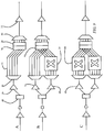
Figure 1 shows an example of a known node
architecture at which amplification and signal routing
functions can take place. For the purposes of clarity,
the components required for transmission from west to
east are shown in Figure 1, although it will be
appreciated that the node will in fact be arranged for
bi-directional flow of traffic. The node 10 receives an
incoming WDM signal from the west and amplifies this
signal using a first amplifier 12. The amplified signal
is provided to a dispersion slope compensation module 14.
A first booster amplifier 16 prepares the signal for the
signal routing part 18 of the node.
There are two amplifiers 12,16 at the input side of
the node because the loss which can be sustained between
two amplifiers is limited. Typically, the dispersion
compensation module 14 may introduce a loss of up to 10dB
and a switching core may introduce a loss of up to 15 dB.
There are, however, numerous other possible
configurations for the amplifier stages.
There is a maximum power per wavelength at which
light can be launched into a fiber before the non-linear
distortions make the signal unusable. This limits the
power of the booster 16, but the power of the booster
amplifier can be increased if it is followed by a linear
loss element (such as a switch). The signal routing part
18 has a wavelength de-multiplexer 20 which divides the
incoming WDM signal into individual channels or groups of
channels 22. These channels 22 are switched by a
switching arrangement 24 which, in addition to routing
signals across the node 10, also provides add and drop
capability, not shown. The switching arrangement is
commonly termed "switching core". The output signals 26
from the switching core 24 are provided to a bank 28 of
variable optical attenuators which are provided for
channel balancing. The balanced channels are then
combined by a multiplexer 30 to define the output of the
signal routing portion 18. This output is then amplified
by a second booster amplifier 32 to define the east bound
output of the node 10.
This node configuration will be well known to those
skilled in the art. In such an arrangement, the
switching core 24 can provide per-channel routing of
signals. However, this switching core 24 is an expensive
component and will not be installed at every amplifier
node where this level of switching capability is not
initially required. However, subsequent changes to the
network may require the switching capability at a node to
be upgraded. Increasing the switching capability also
increases the loss of the signal routing portion 18 so
that the booster amplifier 16 will also require upgrading
to support the increased switching capability.
The node illustrated in Figure 1 is shown in
simplified schematic form. For clarity, Figure 2 shows
the node architecture in which the node can perform
signal routing operations between three fiber spans, to
the east, west and south of the node. Thus, the node
architecture shown in Figure 2 implements a Y-branch.
The incoming fibers from the east, west and south each
undergo amplification, dispersion compensation, first
stage boosting and de-multiplexing using the same
components as described in connection with Figure 1. In
the example shown in Figure 2, each de-multiplexer 20
provides five channels on different respective
wavelengths. In the example shown in Figure 2, the
switching arrangement 24 has individual switching planes
25 for each of the different wavelengths. For example,
the switching plane 25a receives as input the first
channel 22a from each of the multiplexers 20, and each of
these channels 22a are on the same carrier frequency.
This enables the switching arrangement 24 to be designed
as a number of separate switching planes 25, each
designed for a specific wavelength. Furthermore, the
node can be arranged to add or drop signals on
predetermined wavelengths by modification to one of the
switching planes only. The outputs of the switching
arrangement 24 are again provided to a bank 28 of
variable attenuators before being combined by
multiplexers 30 to form the individual east bound, west
bound and south bound signals.
In order to avoid the need to provide full switching
capability when a network is installed, the node
architecture needs to be designed to enable upgrades to
be performed. There is also a need to provide
protection/duplication of equipment to enable repair or
servicing of components within the node.
Summary of the invention
The inventors have firstly recognised the need to
provide protection for the switching arrangement 24, as
it may require servicing or repair, and it may also be
desirable to change some of the switching planes, or to
add new switching planes, to allow different signal
routing capability. One possible way of providing this
protection is shown in Figure 3. In this arrangement,
two switching cores 24a, 24b are provided. An array of
splitters 40 provides the individual channels or groups
of channels 22 on two different paths, each leading to a
different switching arrangement 24. The outputs from the
two switching arrangements 24a, 24b are then applied to a
bank 42 of two-way switches which enable one or other of
the inputs to be routed to the bank of variable optical
attenuators 28. This arrangement enables the switching
core 24 to be replaced for upgrade or maintenance and
provides duplication only of the switching arrangement
itself. By providing two separate paths for the
different switching arrangements 24 protection is
provided, but this protection is not provided for the
bank 28 of attenuators, and this arrangement does not
allow upgrade of the de-multiplexer 20 and multiplexer 30
without interrupting normal service.
One way to overcome these disadvantages is to
provide two full signal routing portions 18a, 18b between
the splitter 40 and the switch 42 as shown in Figure 4.
In this way, the whole signal routing portion 18 is
protected so that the failure of any component within the
signal routing portion 18 is protected and all components
can be upgraded without interrupting service through the
node. However, if a switching arrangement 24 is being
added to a node with no switching capability, this will
normally require upgrade of the first booster amplifier
16, and the arrangement of Figure 4 requires an
interruption of service to enable this upgrade.
According to a first aspect of the invention, there
is provided an optical amplifier arrangement comprising:
In this arrangement, there are two paths between the
input and output. The path in use (the "at least one of
the paths") includes an optical amplifier and a switching
arrangement. Whilst this path is being used, the
components in the other path can be upgraded. For
example, a switching arrangement may be provided in the
other path, and an amplifier may also be upgraded,
without disrupting service in the path in use. This
enables an amplifying node within an optical
communications system to be incrementally upgraded.
For example, the switching arrangement may comprise
at least one wavelength-selective tap for tapping a
selected wavelength channel from the WDM signal. This
wavelength may be dropped or routed to a new span through
a manually-provisioned patch panel. This may be upgraded
in the unused path to a multiple input and multiple
output switching core for automatically routing
individual channels of the WDM signal. This upgrade
requires the amplifier in the path to be upgraded, and
this can also be done without disrupting service in the
path in use. The switch is then controlled to receive
signals from the upgraded path.
The two paths can be upgraded in turn, so that in
the fully upgraded arrangement, a switching core is
provided in each of the first and second output paths,
and each switching core is provided with a wavelength
division de-multiplexer at the input of the core for
dividing the WDM signal into individual channels or
groups of channels.
In one embodiment, the outputs of the switching
cores are provided to the switch, and a wavelength
division multiplexer is provided at the output of the
switch. The switch thus receives individual channels,
and can therefore be arranged as a switch array, which
can select different channels from different paths. This
means that the arrangement can provided per-channel
protection.
Alternatively, each switching core can be provided
with a wavelength division multiplexer at the output of
the core for combining the WDM channels into an
individual WDM signal, and wherein the WDM signals from
the two multiplexers are provided to the switch. The
switch thus switches the WDM signal, so that per-channel
protection is not possible. However, by placing the
multiplexer before the switch, the multiplexer in the
unused path can be upgraded or replaced without
disrupting service.
When each switching core is provided with a
wavelength division multiplexer at the output of the core
for combining the WDM channels into a WDM signal, a
further amplifier may also be provided in each path for
amplifying the WDM signals, the amplified WDM signals
being provided to the switch. The further amplifier
(which is a second booster amplifier) is then
upgradeable.
In some embodiments, the output of the switch is
further amplified before defining the output of the
amplifier arrangement.
According to a second aspect of the invention, there
is provided an optical amplifier arrangement comprising:
A wavelength division multiplexer may also be
provided at the output of the switch.
This arrangement provides the ability to upgrade the
amplifier to a higher power version, thus compensating
for the loss in the switch, and avoids the need to
provide upgraded amplifiers in two separate paths.
The invention also provides an optical
communications system comprising a plurality of nodes
connected by optical transmission lines, wherein at least
one node is provided with an optical amplifier
arrangement according to the invention.
The invention also provides a method of upgrading an
optical amplifier arrangement, comprising defining a
first path between an input and an output of the
amplifier arrangement, the first path including a
splitter;
This method allows a channel routing device to be
installed or upgraded, with installation of the required
booster amplifier, without disrupting operation of the
arrangement. By "routing a signal towards the output" is
meant that the signal ultimately contributes to the
output signal, but that additional operations may be
carried out on the signal before it defines the output of
the optical amplifier arrangement.
For example, the amplified signal may undergo
further amplification before defining the output of the
arrangement.
The method may further comprise upgrading the
amplifier and providing or upgrading a channel routing
device in the first path downstream of said splitter. In
this way, both paths may be upgraded in turn, without
disrupting service, so that the fully upgraded
arrangement can provide 1+1 protection.
The signal is preferably routed from the first or
second path towards the output by a switch.
Brief description of the drawings
Examples of the invention will now be described in
detail with reference to the accompanying drawings in
which:
Detailed description of the invention
in the following detailed description, the invention
is described in connection with one plane through the
node. In the same way that Figure 1 represents one plane
through the node architecture of Figure 2, the invention
is described in connection with one input port, one
output port, and a single switch which will in practice
form part of a multiple plane node architecture with
multiple inputs, multiple outputs, and a multi-plane
switch.
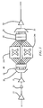
Figure 5 shows a first example of switching
arrangement in accordance with the invention. In the
following examples, this switching arrangement will be
described as a "node", as the arrangement will typically
be used within a node of an optical communication system.
This node is provided for amplification of optical
signals and optionally the routing of signals around the
network.
In the following examples where the same components
are used as described in connection with Figures 1-4, the
same reference numerals will be used.
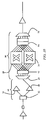
In Figure 5, two paths are provided between a
splitter 40 and a switch 42. Each path includes its own
first booster amplifier 16 and signal routing portion 18.
In this example, the splitter 40 and the switch 42
operate on the combined WDM signal. The splitter 40 is a
3dB coupler which provides equal powers on the two output
branches. The switch 42 is a two way, or 2x1 switch,
which provides at its output the full signal from the
selected input. The switch could also be a 2x2 switch,
which provides at its main output the signal from the
selected path. It also provides at a second output the
signal from the non-selected path through the signal
routing portion 18. This allows monitoring of the
signals flowing through the inactive path, to ensure that
the inactive path is operating correctly before switching
to it.
This arrangement enables one path to be used, by
selecting the appropriate input at switch 42 whilst the
components in the other path can be upgraded or repaired.
This upgrade or repair function will typically involve
adding a switching arrangement 24 and this will require a
corresponding increase in the amplification power of the
first booster amplifier 16. By providing protection both
for the first booster amplifier 16 as well as the signal
routing portion 18, additional upgrade functions can be
performed without disrupting the operation of the node.
The arrangement of Figure 5 allows the frequency
plan to be upgraded. For example, if the first path uses
a 40 lambda system with wavelengths spaced 100GHz apart,
the second upgraded path can be upgraded to use an 80
lambda system with wavelengths spaced 50GHz apart. It
would also allow movement from a banded structure to a
system that used individual wavelength granularity.
By way of example only, Figure 6 shows one possible
upgrade scheme provided by the invention.
Figure 6A shows an amplification site in which no
add/drop capability is initially required. To enable
this amplification site to be upgraded in accordance with
the invention, it is nevertheless provided with the
splitter 40 (the outputs of which may require isolators)
and switch 42, with the booster amplifier 16 between the
splitter 40 and switch 42. Thus, a first path is defined
which includes the splitter 40 and which includes an
amplifier (the first booster amplifier 16) down stream of
the splitter 40. The switch 42 is positioned to route
the amplified signal from the amplifier 16 towards the
output, in particular to the second booster amplifier 32.
Figure 6B assumes that some add/drop capability is
now required at the site of the node, for example as a
result of a population increase at that location. In
order to achieve the adding or dropping of a small number
of wavelengths at lowest cost, a number of optical
add/drop couplers 50 can be provided in the first path,
again between the splitter 40 and the switch 42. During
installation of the components 50 alternative protection
paths through the network can be employed to avoid the
need to disrupt service. Alternatively, the couplers 50
can be installed in the second path, with an associated
amplifier 16 in that path, and the switch 42 is then
switched once the second path is installed.
As the requirement for additional add/drop or signal
routing capability increases, an upgrade is carried out
in the unused path. In the example shown in Figure 6, a
second path is defined, which again includes the splitter
40. An amplifier 60 is provided in the second path
together with a full signal routing portion 18. The
amplifier 60 will typically have a higher power than the
amplifier 16, in order to compensate for the higher loss
of the signal routing portion 18. Traffic can then be
switched to the second path, by controlling the switch 42
to route signals from the second path to the second
booster amplifier 32. This then enables the first path
to be upgraded. In particular, the components 50 are
replaced by a full signal routing portion 18 and the
first booster amplifier 16 is replaced with an amplifier
with a similar specification to that of amplifier 60.
The configuration shown in Figure 6D then corresponds to
that described with reference to Figure 5.
The arrangement of the invention enables an
incremental upgrade operation to be carried out. For
example, the number of switching planes providing
add/drop and signal routing capability can be
incrementally increased, and each time an upgrade is
taking place the switch 42 will select as input the path
not at that time being disrupted.
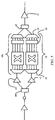
Figure 7 shows a variation to the arrangement of
Figure 5, in which the second booster amplifier 32 is
also duplicated, with one second stage booster amplifier
32 being provided in each of the two paths between the
splitter 40 and the switch 42. The second booster
amplifier 32 is then also upgradeable. Furthermore,
placing the switch 42 after the second booster amplifier
32 removes the loss of the switch from the second mid-stage.
The power of the amplifier 32 can be increased to
compensate for the loss of the switch 42.
The examples above each provide protection for all
components of the signal routing portion 18, to enable
repair or upgrade of any of those components. This is,
however, at the expense of large duplication of
components within the node. Furthermore, the switch 42
in each of the examples above switches the full WDM
signal, so that the protection provided is for the full
switch rather than on a per-channel basis.
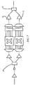
Figure 8 shows a further example of node in
accordance with the invention which enables upgrade of
the switching arrangement 24 but which also provides per-channel
protection. In this example, the two paths are
provided between the splitter 40, which acts on the full
WDM signal, and a bank 70 of switches which enables
switching of the individual channels or groups of
channels. In this case, the bank 70 of switches receives
the outputs from the two switching arrangements 24 and
can select on an individual channel (or channel group)
basis which of the two paths to route to the bank 28 of
variable optical attenuators. A single multiplexer 30 is
thus provided down stream of the bank 70 of switches, the
output of which is provided to the second booster
amplifier 32. With this arrangement, the multiplexer 30
cannot be upgraded without interrupting service. As a
result, the initial node configuration must include full
de-multiplexing and multiplexing to enable subsequent
upgrades to be carried out without modifying the
multiplexer 30.
Figure 9 illustrates one example of upgrade method
to provide the node configuration of Figure 8. In Figure
9A, even though no switching capability is initially
required, the first path between the splitter 40 and the
bank 70 of switches is nevertheless provided with a demultiplexer
20 to provide the individual channels or
groups of channels 22. This full break out of channels
allows add/drop and signal routing connections to be
manually configured using a fiber patch panel. A normal
first booster amplifier 16 will provide the required
amplification taking into account the loss resulting from
the de-multiplex and subsequent multiplex operation.
When upgrade of this node is required, the second
path is defined and is provided with a switching core 24
having add/drop and signal routing capability. A higher
power first booster amplifier 60 will be required to
compensate for the loss of the switching core 24. When
the second path has been upgraded, the bank 70 of
switches is controlled to receive signals from the second
path, which in turn allows upgrade of the first path to
provide the add/drop and signal routing capability. This
involves providing a switching core 24 in the first path
and upgrading the first booster amplifier 16 to provide
amplifier 60, as shown in Figure 9C.
The arrangement of Figure 9 enables per-channel
protection as well as upgrade of the switching core 24.
This is again achieved with a single splitter 40 and a
single bank 70 of switches. By duplicating the first
booster amplifier 60 in each of the paths between the
splitter 40 and the bank of switches 70, there is
duplication of the high power first booster amplifier 60.
It may be beneficial to duplicate the high power
booster amplifier, which is less reliable than a normal
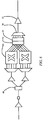
amplifier. However, Figure 10 shows an alternative
arrangement which also provides per-channel protection as
well as the capability of upgrading the switching core,
but which does not require two high power first booster
amplifiers 60. The arrangement of Figure 10 effectively
comprises an amplifier section 80 and a switching core
section 90. The amplifier section 80 has a first
splitter 82 which provides the input WDM signal on to two
paths. Within one of these paths is a low power first
booster amplifier 16 which has a power sufficient for the
initial configuration of the node in which add/drop
capability is provided through a manual patch panel, but
no switch is required. The second path has a higher
power first booster amplifier 60 having sufficient power
for the configuration in which a switch is provided. In
the initial configuration of the node, the output from
the low power first booster amplifier 16 is provided to
the demultiplexer and patch panel arrangement (manual
routing arrangement), whereas when the upgrade from the
manual routing arrangement to the automatic switching
core section 90 is carried out, the high power booster
amplifier 60 is first installed and the output from that
amplifier is connected to the switching core section 90
once it has been installed.
The switching core section 90 has a bank 92 of
splitters and a bank 94 of switches surrounding two
optical switching arrangements 24 to provide per-channel
protection. The de-multiplexer 20 and multiplexer 30 are
provided outside the branched pair of paths and are
therefore not upgradeable.
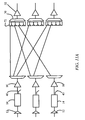
Figure 11 shows in greater detail the upgrade
operation of Figure 10 in which traffic is controlled by
the node bi-directionally between three directions, east
west and south. When the network is initially installed,
the channel connections between the different paths are
hard wired into the node, as shown in Figure 11A, using a
patch panel
In this example, each bank 70 of switches has been
integrated with the bank 28 of variable optical
attenuators to provide the combined component 72
illustrated. In order to upgrade the node, the higher
power first booster amplifiers 60 are installed and
coupled to the splitters 40 as shown in Figure 11B. The
switching core 24 is then installed together with a bank
of splitters 25 at the inputs of the switching core 24.
The outputs of the switching core 24 are coupled to the
bank 72 of switches and optical attenuators, as shown in
Figure 11C.
It is then possible to strip out the patch panel.
The bank 72 is then controlled to receive signals from
the switching core 24, thereby enabling a second
switching core to be installed. This involves
incorporating a second switching core 24 and connecting
it to the new bank of splitters 25, as shown in Figure
11D..
Figure 12 shows in schematic form one possible way
of implementing the node architecture in hardware. As
shown in Figure 12, each switch plane (such as 25 in
Figure 2) is implemented as a switch card 100 having
inputs 102 and outputs 104 along an edge 106. Each
switch card 100 may be for an individual wavelength or
for a group of wavelengths. The two de-multiplexers 20
are provided on a first board 108 and provide the
individual channel or channel group ports along an edge
110. These ports define a first series 112 for one path
(for example the working path) and a second series 114
for the other path (for example the protect path).
The bank 70 of switches and the bank 28 of optical
attenuators, together with the multiplexer 30 are
provided on a second board 120, again providing
individual working and protect channels or groups of
channels in series 122 and 124. These series of
individual channels or channel groups are arranged in the
same order for the two cards 108, 120 so that a single
switch plane 100 can interconnect all channels of the
same wavelength for all boards. For example, a
connection 130 is established where the edge 106 of the
switch plane 100 meets the edge 110 of the board 108.
The orthogonal card-to-card connections should be made
through blind mate fiber optic connectors. These might
be single fiber or multi-fiber connectors.
In the examples above, the multiplexers and de-multiplexers
are shown as a single component, but they
may be multi-stage components using interleaving
operations. More specific details of the manner in which
the node architecture may be implemented will be apparent
to those skilled in the art.
As discussed above, the amplifier arrangement of the
invention may be used in a node of an optical
communications system. Such a system comprises a
plurality of nodes connected by optical transmission
lines wherein at least one node which is an intermediate
node, is provided with an optical amplifier and signal
routing arrangement of the invention.
Although the amplifier arrangement has been
described in use in a node, it may find uses in other
parts of a network. The splitter and the switch used in
the design may take various forms, and are well known and
used components. The splitter is any device for
providing an input onto two different outputs.
In the examples above, the splitter provides the
input on both outputs, so that protection switching may
be implemented by operating the switch only. However, it
is equally possible for the splitter to comprise a
switch, so that the input is selectively provided on one
or other output. This will result in a lower loss
component, but means that both the splitter and the
switch must be controlled to enable use of the second
path for protection or to enable upgrade of the main
path. Another benefit of providing the splitter output
on both paths simultaneously is that signals are provided
to the protection paths so that the protection path can
be tested before switching to it. However, the term
"splitter" is intended to cover any component which
enables an input to be provided on at least two outputs,
whether simultaneously or selectively, possibly with
isolators. It also covers a single input or multiple
input device.
There are a large number of possible designs for the
optical amplifiers used within the arrangement, and these
will depend on the particular signal traffic through the
switching arrangement. Amplification is often carried
out using Erbium doped amplifiers- these may be fiber
based or waveguide based, and other rare-earth dopants
can be used, for example Thulium and Ytterbium. Raman
amplifiers are also known for use in broadband
amplification systems.
The switching arrangements may be all optical or
they may be hybrid systems, in which the switching takes
place in the electrical domain. In all optical systems,
the switching operation is effectively a reflection, for
example using arrays of MEM (micro-mechanical mirrors).
All of these possibilities are intended to be within
the scope of the invention as claimed.
The use of Variable Optical Attenuators has been
described above for channel balancing. As an
alternative, per channel amplifiers can be used either in
addition to the VOAs or instead of them. The signal
routing portion may also include discrete per channel or
per band amplifiers to mitigate some more of the loss.
Only a small variety of specific node configurations
have been shown. The invention will be of benefit to any
node configuration in which there is at least one booster
amplifier before the signal routing section.