EP1316913A2 - Capacitive fingerprint sensor with protective coating containing a conductive suspension - Google Patents
Capacitive fingerprint sensor with protective coating containing a conductive suspension Download PDFInfo
- Publication number
- EP1316913A2 EP1316913A2 EP02257814A EP02257814A EP1316913A2 EP 1316913 A2 EP1316913 A2 EP 1316913A2 EP 02257814 A EP02257814 A EP 02257814A EP 02257814 A EP02257814 A EP 02257814A EP 1316913 A2 EP1316913 A2 EP 1316913A2
- Authority
- EP
- European Patent Office
- Prior art keywords
- protective coating
- sensing
- conductive particles
- sensor device
- fingerprint sensor
- Prior art date
- Legal status (The legal status is an assumption and is not a legal conclusion. Google has not performed a legal analysis and makes no representation as to the accuracy of the status listed.)
- Granted
Links
Images

Classifications
-
- G—PHYSICS
- G06—COMPUTING OR CALCULATING; COUNTING
- G06V—IMAGE OR VIDEO RECOGNITION OR UNDERSTANDING
- G06V40/00—Recognition of biometric, human-related or animal-related patterns in image or video data
- G06V40/10—Human or animal bodies, e.g. vehicle occupants or pedestrians; Body parts, e.g. hands
- G06V40/12—Fingerprints or palmprints
- G06V40/13—Sensors therefor
- G06V40/1329—Protecting the fingerprint sensor against damage caused by the finger
-
- G—PHYSICS
- G06—COMPUTING OR CALCULATING; COUNTING
- G06V—IMAGE OR VIDEO RECOGNITION OR UNDERSTANDING
- G06V40/00—Recognition of biometric, human-related or animal-related patterns in image or video data
- G06V40/10—Human or animal bodies, e.g. vehicle occupants or pedestrians; Body parts, e.g. hands
- G06V40/12—Fingerprints or palmprints
- G06V40/13—Sensors therefor
- G06V40/1306—Sensors therefor non-optical, e.g. ultrasonic or capacitive sensing
Definitions
- the present invention relates generally to protective coatings for semiconductor devices, and more particularly to the surface structure of solid-state fingerprint sensors.
- a capacitive fingerprint sensor is disclosed in commonly-assigned U.S. Patent No. 6,114,862 by Tartagni et al. , the disclosure of which is hereby incorporated by reference.
- the Tartagni et al. patent discloses a two-dimensional array of capacitive sensor cells or "pixel" cells.
- the array includes a dielectric layer that forms a sensing surface for contact with the fingerprint-bearing skin of a user's finger.
- Capacitor plates at each pixel location beneath the dielectric layer distinguish between the presence of fingerprint ridges and valleys above the sensing surface during a fingerprint sensing operation.
- the dielectric layer that forms the sensing surface in prior art fingerprint sensors is typically an ultra-hard material that is resistive to wear from repeated use.
- an ultra-hard dielectric material used in prior art fingerprint sensors is a layer of silicon carbide. It has been found that such ultra-hard dielectric layers can be damaged by impact with sharp instruments, such as the point of a ballpoint pen. Although it is impractical to design a product that will survive intentional destructive misuse, it is desirable to design a product that will survive occasional accidental misuse. Therefore, it would be desirable to find a material for use as a protective coating for a fingerprint sensor that is durable with normal expected use, resistive to occasional accidental misuse, and effective in permitting accurate sensing of a fingerprint of a finger applied to a sensing surface.
- the present invention provides a protective coating for a fingerprint sensor that comprises a polymeric material with conductive particles suspended therein.
- the protective coating has an exposed upper surface for contact with the fingerprint-bearing skin of a user's finger.
- the protective coating is durable and resistive to damage from scratching or impact from a sharp or pointed object.
- the protective coating is applied to an underlying hard dielectric body that includes capacitive sensing plates embedded therein.
- the conductive particles suspended in the protective coating are generally uniformly distributed and are smaller than the thickness of the protective coating so that they define parallel strings of series capacitors between the upper sensing surface of the protective coating and the capacitive sensing plates disposed beneath the protective coating at each pixel location.
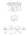
- a portion of an array 10 of sensing elements 12 is shown defining pixel locations within a fingerprint sensor device.
- the sensing elements 12 are arranged in rows and columns of sufficient number to create an image of a fingerprint.
- the sensing elements 12 are disposed beneath a sensing surface 14 to which the fingerprint-bearing skin of a user' s finger is applied during a sensing operation.
- the sensing elements 12 are arranged with a center-to-center spacing of about 50 microns, column-to-column and row-to row, throughout the array 10.
- the cross-sectional structure of a portion of the pixel array 10 is shown schematically in relationship to a user's finger 16.
- the finger 16 has fingerprint-bearing skin 18 that includes ridges 20 and valleys 22, which are common characteristics of human fingerprints but are uniquely patterned for each individual.
- the ridges 20 are shown in contact with the sensing surface 14, and the valleys 22 are spaced just above the sensing surface 14.
- the fingerprint sensor of which the array 10 is a part is formed on a semiconductor substrate 24, which may consist essentially of monocrystalline silicon doped to a specified resistivity.
- An epitaxial layer 26 is formed atop the substrate 24 and is considered part of the substrate 24.
- Active circuitry which may consist mainly of interconnected MOS transistors (not shown), is formed in the epitaxial layer 26 using conventional semiconductor manufacturing techniques. An example of suitable active circuitry formed in the epitaxial layer 26 is described below with reference to FIG. 5.
- the sensing elements 12 communicate with the active circuitry in the epitaxial layer 26 through conductive paths 28, depicted generally in FIG. 2.
- the sensing elements 12 and conductive paths 28 are formed in a composite dielectric body 30, which typically includes multiple layers of oxide, nitride or other conventional dielectric materials used in semiconductor device fabrication.
- the composite dielectric body 30 has an upper surface 32.
- the sensing elements 12 extend to the upper surface 32 from a depth therebelow.
- a protective coating 34 Disposed atop the upper surface 32 of the composite dielectric body 30 is a protective coating 34 that includes multiple conductive particles 36 suspended therein.
- the sensing element 12 preferably is a capacitive sensing element.
- the capacitive sensing element 12 includes an upper capacitor plate 38 lying at the upper surface 32 of the composite dielectric body 30.
- the sensing element 12 further includes a first lower capacitor plate 40 and a second lower capacitor plate 42, which are coplanar and are arranged beneath the upper plate 38 to define respective first and second capacitors therewith.
- a thin dielectric layer 44 which is a portion of the composite dielectric body 30, separates the upper capacitor plate 38 from the first and second lower capacitor plates 40 and 42.
- the thin dielectric layer 44 is preferably from 0.2 to 0.3 microns thick and may comprise silicon nitride, phosphosilicate glass or other such commonly used dielectric materials.
- a narrow gap 46 is formed between the facing edges of the lower plates 40 and 42. The gap 46 is about 1 to 2 microns wide and is filled with dielectric material.
- the first and second lower plates 40 and 42 preferably occupy an area that corresponds to and is juxtaposed beneath the upper plate 38. Such an arrangement advantageously minimizes the parasitic capacitance between the upper plate 38 and ground.
- Conductors 48 and 50 connect respective plates 40 and 42 to the active circuitry in the epitaxial layer 26 of the substrate 24. The conductors 48 and 50 correspond to one of the conductive paths 28 described above with reference to FIG. 2.
- the upper plate 38 need not be in direct contact with the protective coating 34.
- the structure could include a very thin polymeric layer (for example, less than 2 microns thick) between the surface 32 and the protective coating 34, the very thin polymeric layer serving as a second protective coating.
- This second very thin protective coating would be essentially free of conductive particles and would be permanently affixed to the surface 32 to protect the composite dielectric body 30 and sensing elements 12.
- the protective coating 34 with suspended conductive particles 36 therein could be replaced if damaged or after excessive wear. This would permit extending the useful life of the fingerprint-sensing device.
- the plates 38, 40, and 42 may be made from conventional metal layers, which are typically aluminum, deposited at two different levels during fabrication of the device. Other conductive materials can be used.
- plate 38 can comprise titanium oxide or a titanium oxide layer atop an aluminum layer.
- plates 40 and 42 can be formed from a conductive polysilicon layer, such as silicided polysilicon.
- the areas shared by the plate 38 and the underlying plates 40 and 42 are sufficiently large that the two capacitors they form each has a much greater capacitance than the capacitor formed between the facing edges of lower plates 40 and 42.
- the protective coating 34 preferably comprises a fluoropolymer that is durable and scratch resistant.
- fluoropolymers are well suited for this application.
- DuPont sells fluorinated ethylene propylene coatings under its brand Teflon® FEP, which are highly hydrophobic and oleophobic, and therefore inhibit retention of fingerprints from skin oil on the sensing surface 14.
- Successful experiments have been performed using a DuPont coating type 958-203, which is a fluoropolymer containing carbon black particles.
- conductive particles 36 Suspended within the protective coating are conductive particles 36 of conductive material or metal, which preferably are generally spherical in shape, although other shapes can function effectively.
- Suitable materials for the conductive particles include carbon, graphite, silicon, aluminum, copper and silver. It is known from analysis of DuPont coating type 958-203 that carbon in the form of carbon black particles can be generally uniformly distributed within a fluoropolymer coating.
- the particles 36 can comprise conductive crystals, such as doped silicon microcrystals. Other conductive materials may be employed.
- the conductive particles 36 can each comprise a particle having a conductive core with a thin outer dielectric coating.
- the conductive particles 36 can be balls of aluminum, each having a thin aluminum oxide film defining an exterior surface.
- a preferred thickness for the protective coating 34 is from 10 to 20 microns. Such a thickness is desirable, not only for its manufacturability and its stress-spreading capability, but also for good image sensitivity and resolution. Preferably, to achieve good image sensitivity and resolution, the thickness of the protective coating 34 should not exceed one-half of the center-to-center spacing between sensing elements 12 of the array 10.
- the protective coating 34 with the conductive particles 36 generally uniformly distributed therein can be applied at the final stage of conventional wafer fabrication. Wafers having multiple sensor devices formed on a common substrate can be prepared by masking off bonding pads on the device surfaces, spraying on the protective coating, allowing the coating to harden, slicing the wafer into chips, uncovering the bonding pads, mounting each chip in protective housing or "package,” wire bonding the chip's bonding pads to terminals within the package, and sealing the package leaving the sensing surface exposed. Similar techniques are commonly practiced in semiconductor device manufacturing.
- the conductive particles 36 should be generally uniform in size and be significantly smaller in diameter (or largest dimension for non-spherical particles) than the thickness of the protective coating 34.
- the conductive particles 36 should have diameters typically of about 5 microns. That is, the diameter or largest dimension the conductive particles 36 ideally should be about one-third the thickness of the protective coating 34. It is not necessary that all such particles 36 be approximately the same size, but best results will be achieved if the larger particles have diameters or largest dimensions that do not exceed one-half of the thickness of the protective coating 34. It is believed that best results will be achieved if more than 90 percent of the particles 36 are sized such that their largest dimension is from one-fourth to one-third of the thickness of the protective coating 34.
- FIG. 4 shows a simplified equivalent circuit that includes a plurality of capacitors arranged in series strings, many such strings being arranged in parallel per pixel. Although three strings of three capacitors each are shown for the pixel corresponding to the plate 38, generally there will be many more such strings, and there may be more or less than three capacitors per string at each pixel location.
- the capacitor strings extend from the upper capacitor plate 38 (seen in FIG. 3) to the sensing surface 14 (seen in FIG. 2).
- the capacitors in FIG. 4 are formed by the conductive particles 36 shown in FIGS. 2 and 3.
- the upper plate 38, the conductive particles 36 disposed thereover, and the sensing surface 14 form a sensing capacitor C s .
- the conductive particles 36 have the electrical effect of making the sensing surface 14 appear much closer to the upper plate 38 than the actual separation distance between them.
- the capacitance of capacitor C s varies with the characteristics of the fingerprint-bearing skin 18 applied to the sensing surface 14 immediately above the upper plate 38 of each pixel. The capacitance is greater when a ridge 20 rather than a valley 22 is present at the sensing surface 14 over a particular sensing element 12.
- the circuitry dedicated to one pixel includes an input node 52, an output node 54, and the circuit elements therebetween.
- Input circuitry 56 selectively connects the input node 52 to a reference voltage source V r .
- the output node 54 is connected to output circuitry 58 that senses output signals from the pixel periodically.
- the output of the pixel at node 54 is generated by an inverting amplifier or charge integrator I, which is similar to the inverting amplifier of U.S. Patent No. 6,114,862 with a different feedback arrangement, as described below.
- the charge integrator I integrates the charge appearing at its negative (-) input and generates a corresponding amplified analog output.
- Series connected capacitors C 1 and C 2 interconnect the pixel's input node 52 with a node 60 that corresponds to the charge integrator's negative (-) input.
- the charge integrator's positive (+) input is connected to a voltage source such as ground.
- the connection between capacitors C 1 and C 2 defines an electrically floating node 62 that also defines a point of connection between capacitors C s and C p .
- Capacitor C p represents the parasitic capacitance that exists between the floating node 62 and the ground node.
- the ground symbols in FIG. 5 may represent the actual ground terminal of the fingerprint sensing device or may represent a
- capacitor C 1 is formed by plate 40 and the portion of plate 38 lying thereover
- capacitor C 2 is formed by plate 42 and the portion of plate 38 lying thereover.
- Capacitor C s is the pixel's sensing capacitor that is formed between the upper plate 38 and the sensing surface 14 (seen in FIG. 2). The capacitance of capacitor C s varies with the presence of ridges and valleys of the skin of the user's finger applied to the sensing surface 14 during a sensing operation.
- a reset switch 64 (seen in FIG. 5) is opened to prepare the charge integrator I to generate an accurate output signal during the sensing operation.
- the reset switch 64 may be a conventional transistor, such as an NMOS transistor, and interconnects the charge integrator's input node 60 and output node 54.
- a feedback capacitor C fb is included in the circuit and couples the charge integrator's output node 54 to its input node 60.
- the device designer can select the capacitance value of feedback capacitor C fb to tune the gain of the charge integrator I to a predetermined desired level.
- Capacitor C fp may be formed in any suitable manner, and may comprise, for example, metal plates at two different levels, or a metal plate disposed over a conductive polysilicon layer, or a conductive polysilicon layer disposed over a heavily-doped surface region in the epitaxial layer 26 of the substrate 24. In whatever form, the capacitor C fp should have a predetermined value maintained within a tight tolerance.
- capacitor C in is connected between the charge integrator's input node 60 and ground
- capacitor C out is connected between the charge integrator' s output node 54 and ground.
- the pixel of FIG. 5 can be considered as having two stages: a capacitive sensing stage comprising capacitors C s , C 1 , C 2 , and C p ; and an amplifier stage comprising the charge integrator I, feedback capacitor C fb , reset transistor switch 64, and the parasitic capacitors C in and C out .
- the reference voltage source V r , input circuitry 56, and the output circuitry 58 are shared by the various pixels of the fingerprint sensor array.
- the pixel is periodically interrogated or "read” in a sequence that individually interrogates each pixel in the entire array of similar such pixels.
- the array 10 can be addressed in a way similar to the way a random access memory chip is addressed, using row and column decoders.
- Address decoder circuitry (not shown) can select individual pixels for interrogation one at a time in a predetermined sequence.
- the pixel takes its turn in the addressing sequence when an input pulse signal ⁇ V generated by reference voltage source V r is applied to capacitor C 1 .
- the pulse ⁇ V propagates through the series-connected capacitors C 1 and C 2 to node 60, where it appears as a transient increase in charge that is input to the charge integrator I.
- the charge integrator's output signal at node 54 is the product of the reference voltage input pulse ⁇ V and the gain of the charge integrator I.
- the output circuitry 58 creates a digitized value of the analog output appearing at node 54. It will be appreciated that the output circuitry 58 will include an analog-to-digital converter (not shown) for converting the analog pixel outputs to digital signals for output off the chip for processing by a system processor or computer.
- Each individual pixel of the sensing array typically occupies an area of about 50 microns by 50 microns.
- the entire sensing surface of which surface 14 is a part is rectangular and has dimensions of 12.8 mm by 18.0 mm.
- there may be over 90,000 pixels in a typical fingerprint sensor which enables a very high resolution of the digitized fingerprint image to be achieved. Since an individual pixel can be addressed and its output read in less than a microsecond, an entire fingerprint image can be captured in less than one-tenth of a second.
- Each of the digitized values of the pixel outputs can be stored in a memory or compared to previously stored fingerprint data in memory. A gray scale image of a detected or previously stored fingerprint can be output to a display screen if desired for visual inspection.
- the protective coating 34 described above can be employed with various configurations of sensing elements and sensing circuitry.
- the inclusion of conductive particles in a thin polymeric coating is particularly useful in capacitive fingerprint sensors, as described herein.
Landscapes
- Engineering & Computer Science (AREA)
- Human Computer Interaction (AREA)
- Physics & Mathematics (AREA)
- General Physics & Mathematics (AREA)
- Multimedia (AREA)
- Theoretical Computer Science (AREA)
- Measurement Of Length, Angles, Or The Like Using Electric Or Magnetic Means (AREA)
- Image Input (AREA)
- Measurement Of The Respiration, Hearing Ability, Form, And Blood Characteristics Of Living Organisms (AREA)
Abstract
Description
phosphosilicate glass or other such commonly used dielectric materials. A
Claims (15)
- A sensor device, comprising:a semiconductor substrate;a dielectric body disposed on the substrate and having a flat upper surface;an array of sensing elements formed in the dielectric body proximate to its upper surface; anda protective coating disposed on the upper surface of the dielectric body over the sensing elements, the protective coating having a flat upper surface defining a sensing surface of the device, the protective coating having conductive particles suspended therein, the conductive particles being distributed within the protective coating to define parallel strings of series capacitors between the sensing surface and each sensing element therebelow.
- The sensor device of Claim 1 wherein each sensing element is a capacitive sensing element having a capacitor plate disposed at the upper surface of the dielectric body.
- A fingerprint sensor device, comprising:an array of capacitive sensing elements, each element having capacitor plate defining one plate of a variable capacitor;a protective coating disposed over the capacitor plate, the protective coating having an upper sensing surface for contact by the fingerprint-bearing skin of a user's finger;the protective coating comprising a polymeric material having conductive particles suspended therein, the protective coating having a uniform thickness, the majority of the conductive particles having a largest dimension that is less than half the thickness of the protective coating; andthe conductive particles being distributed with sufficient density within the protective coating to define parallel strings of series capacitors between the upper sensing surface and each capacitor plate therebelow.
- The fingerprint sensor device of Claim 3 wherein the majority of the conductive particles have largest dimensions that are from one-quarter to one-third the thickness of the protective coating.
- The fingerprint sensor device of Claim 3 wherein the polymeric material comprises at least one of a fluoropolymer and fluorinated ethylene propylene.
- The fingerprint sensor device of Claim 3 wherein the conductive particles are generally spherically shaped.
- The fingerprint sensor device of Claim 1 or 3 wherein the conductive particles comprise conductive material selected from the group consisting of carbon, graphite, silicon, aluminum, copper, and silver.
- The fingerprint sensor device of Claim 3 further comprising a thin polymeric layer is interposed between the protective coating and the capacitor plates of the sensing elements, the thin polymeric layer being less than 2 microns thick.
- A fingerprint sensor device for sensing the fingerprint-bearing skin of a user's finger and generating digitized signals from which an image of the fingerprint can be created, the device comprising:a semiconductor substrate;a plurality of pixels formed at locations above the substrate, the pixels being uniformly spaced apart by a predetermined center-to-center spacing;a dielectric body disposed on the substrate and having an upper surface, the dielectric body having capacitor plates embedded therein, the capacitor plates including upper capacitor plates lying at the upper surface, each upper capacitor plate corresponding to a pixel location and defining a portion of a capacitive sensing stage for each pixel;active circuitry formed in the substrate including an amplifier stage for each pixel, each amplifier stage connected to its pixel's capacitive sensing stage for generating an amplified output signal that is a function of a fingerprint characteristic that occurs at the respective pixel when a user's finger is applied to the device; anda protective coating disposed over the dielectric body, the protective coating having a uniform thickness and including a plurality of conductive particles distributed therein, the protective coating having an upper surface defining a sensing surface of the device to which the fingerprint-bearing skin of a user's finger is applied during a sensing operation, the sizes of a majority of the conductive particles being less than one-half the thickness of the protective coating, the density of the conductive particles within the protective coating being sufficiently large to create capacitors within the protective coating at each pixel location of the device to couple the capacitance defined by the user's skin applied to the sensing surface to the pixel's capacitive sensing stage therebelow.
- The fingerprint sensor device of Claim 9 wherein the capacitive sensing stage of each pixel includes first and second capacitors connected in series, the first and second capacitors being defined by the upper capacitor plate and respective first and second lower plates embedded in the dielectric body beneath the upper plate, the upper capacitor plate defining a common node of the series first and second capacitors, the upper capacitor plate and the conductive particles thereover defining a sensing capacitor whose capacitance varies with the fingerprint characteristics of the user's finger applied to the sensing surface thereover at the respective pixel location.
- The fingerprint sensor device of Claim 9 wherein the protective coating comprises a fluoropolymer and the thickness of the protective coating is less than one-half the center-to-center pixel spacing.
- The sensor device of Claim 1 or 9 wherein the thickness of the protective coating is from 10 to 20 microns.
- The fingerprint sensor device of Claim 9 wherein at least 90 percent of the conductive particles have largest dimensions that are from one-quarter to one-third the thickness of the protective coating.
- The fingerprint sensor device of Claim 1 or 9 wherein the protective coating comprises at least one of fluorinated ethylene propylene and a fluoropolymer.
- The fingerprint sensor device of Claim 9 wherein the conductive particles have conductive cores covered by a thin outer dielectric coating.
Applications Claiming Priority (2)
| Application Number | Priority Date | Filing Date | Title |
|---|---|---|---|
| US10/000,174 US6693441B2 (en) | 2001-11-30 | 2001-11-30 | Capacitive fingerprint sensor with protective coating containing a conductive suspension |
| US174 | 2001-11-30 |
Publications (3)
| Publication Number | Publication Date |
|---|---|
| EP1316913A2 true EP1316913A2 (en) | 2003-06-04 |
| EP1316913A3 EP1316913A3 (en) | 2006-08-23 |
| EP1316913B1 EP1316913B1 (en) | 2008-03-05 |
Family
ID=21690259
Family Applications (1)
| Application Number | Title | Priority Date | Filing Date |
|---|---|---|---|
| EP02257814A Expired - Lifetime EP1316913B1 (en) | 2001-11-30 | 2002-11-12 | Capacitive fingerprint sensor with protective coating containing a conductive suspension |
Country Status (4)
| Country | Link |
|---|---|
| US (1) | US6693441B2 (en) |
| EP (1) | EP1316913B1 (en) |
| JP (1) | JP4308508B2 (en) |
| DE (1) | DE60225407T2 (en) |
Cited By (9)
| Publication number | Priority date | Publication date | Assignee | Title |
|---|---|---|---|---|
| WO2007078678A1 (en) * | 2005-12-30 | 2007-07-12 | Cardinal Health 303, Inc. | Optical fingerprint imaging system and method with protective film |
| WO2010120646A1 (en) * | 2009-04-15 | 2010-10-21 | Authentec, Inc. | Thinned finger sensor and associated methods |
| US8487624B2 (en) | 2008-09-01 | 2013-07-16 | Idex Asa | Surface sensor |
| WO2014195429A1 (en) * | 2013-06-07 | 2014-12-11 | Morpho | Device for capturing an image representing an impression of a body part of a person |
| US9122901B2 (en) | 2009-12-29 | 2015-09-01 | Idex Asa | Surface sensor |
| WO2015134164A1 (en) * | 2014-03-04 | 2015-09-11 | Apple Inc. | Field shaping channels in a substrate above a biometric sensing device |
| EP3370187A4 (en) * | 2017-01-19 | 2018-10-31 | Shenzhen Goodix Technology Co., Ltd. | Fingerprint recognition device |
| EP2959430B1 (en) * | 2013-02-22 | 2019-03-27 | Idex Asa | Integrated fingerprint sensor |
| WO2024239906A1 (en) * | 2023-05-19 | 2024-11-28 | 京东方科技集团股份有限公司 | Display panel and display apparatus |
Families Citing this family (84)
| Publication number | Priority date | Publication date | Assignee | Title |
|---|---|---|---|---|
| US7316167B2 (en) * | 2000-05-16 | 2008-01-08 | Fidelica, Microsystems, Inc. | Method and apparatus for protection of contour sensing devices |
| JP2003093370A (en) * | 2001-09-26 | 2003-04-02 | Sony Corp | Fingerprint detection device |
| US6927581B2 (en) * | 2001-11-27 | 2005-08-09 | Upek, Inc. | Sensing element arrangement for a fingerprint sensor |
| US6941004B2 (en) * | 2001-12-06 | 2005-09-06 | Motorola, Inc. | Method and apparatus for asperity sensing and storage |
| US20040115823A1 (en) * | 2002-12-12 | 2004-06-17 | Potyrailo Radislav Alexandrovi | Method for improvement of environmental stability and selectivity of materials for sensors |
| WO2005031636A1 (en) * | 2003-09-24 | 2005-04-07 | Authentec, Inc. | Finger biometric sensor with sensor electronics distributed over thin film and monocrystalline substrates and related methods |
| US8165355B2 (en) | 2006-09-11 | 2012-04-24 | Validity Sensors, Inc. | Method and apparatus for fingerprint motion tracking using an in-line array for use in navigation applications |
| US8229184B2 (en) | 2004-04-16 | 2012-07-24 | Validity Sensors, Inc. | Method and algorithm for accurate finger motion tracking |
| US8358815B2 (en) | 2004-04-16 | 2013-01-22 | Validity Sensors, Inc. | Method and apparatus for two-dimensional finger motion tracking and control |
| US8175345B2 (en) | 2004-04-16 | 2012-05-08 | Validity Sensors, Inc. | Unitized ergonomic two-dimensional fingerprint motion tracking device and method |
| US8447077B2 (en) | 2006-09-11 | 2013-05-21 | Validity Sensors, Inc. | Method and apparatus for fingerprint motion tracking using an in-line array |
| US8131026B2 (en) | 2004-04-16 | 2012-03-06 | Validity Sensors, Inc. | Method and apparatus for fingerprint image reconstruction |
| WO2005106774A2 (en) | 2004-04-23 | 2005-11-10 | Validity Sensors, Inc. | Methods and apparatus for acquiring a swiped fingerprint image |
| DE602005022900D1 (en) | 2004-10-04 | 2010-09-23 | Validity Sensors Inc | FINGERPRINTER CONSTRUCTIONS WITH ONE SUBSTRATE |
| US20060129839A1 (en) * | 2004-12-13 | 2006-06-15 | Jun Ye | Flexchip-mounted fingerprint sensor |
| US7339448B2 (en) * | 2004-12-14 | 2008-03-04 | Freudenberg-Nok General Partnership | Water resistant encoding material |
| US7849751B2 (en) * | 2005-02-15 | 2010-12-14 | Clemson University Research Foundation | Contact sensors and methods for making same |
| US7193423B1 (en) * | 2005-12-12 | 2007-03-20 | International Business Machines Corporation | Wafer-to-wafer alignments |
| US20080079442A1 (en) * | 2006-08-31 | 2008-04-03 | Joshua Posamentier | Quantum tunneling biometric identification methods and apparatuses |
| CN100535648C (en) * | 2006-09-12 | 2009-09-02 | 吕志刚 | Damage detection information smart coat with subsidiary damage feature |
| US7584068B2 (en) * | 2007-02-22 | 2009-09-01 | Teradyne, Inc. | Electrically stimulated fingerprint sensor test method |
| US8107212B2 (en) | 2007-04-30 | 2012-01-31 | Validity Sensors, Inc. | Apparatus and method for protecting fingerprint sensing circuitry from electrostatic discharge |
| US8290150B2 (en) | 2007-05-11 | 2012-10-16 | Validity Sensors, Inc. | Method and system for electronically securing an electronic device using physically unclonable functions |
| US20090155456A1 (en) * | 2007-12-14 | 2009-06-18 | Validity Sensors, Inc. | System and Method for Fingerprint-Resistant Surfaces for Devices Using Fingerprint Sensors |
| US8204281B2 (en) | 2007-12-14 | 2012-06-19 | Validity Sensors, Inc. | System and method to remove artifacts from fingerprint sensor scans |
| US8276816B2 (en) | 2007-12-14 | 2012-10-02 | Validity Sensors, Inc. | Smart card system with ergonomic fingerprint sensor and method of using |
| US8116540B2 (en) | 2008-04-04 | 2012-02-14 | Validity Sensors, Inc. | Apparatus and method for reducing noise in fingerprint sensing circuits |
| EP2321764A4 (en) | 2008-07-22 | 2012-10-10 | Validity Sensors Inc | System, device and method for securing a device component |
| US8391568B2 (en) | 2008-11-10 | 2013-03-05 | Validity Sensors, Inc. | System and method for improved scanning of fingerprint edges |
| US8600122B2 (en) | 2009-01-15 | 2013-12-03 | Validity Sensors, Inc. | Apparatus and method for culling substantially redundant data in fingerprint sensing circuits |
| US8278946B2 (en) | 2009-01-15 | 2012-10-02 | Validity Sensors, Inc. | Apparatus and method for detecting finger activity on a fingerprint sensor |
| US8374407B2 (en) | 2009-01-28 | 2013-02-12 | Validity Sensors, Inc. | Live finger detection |
| US8820173B2 (en) | 2009-03-06 | 2014-09-02 | Andrew C. Clark | Contact sensors and methods for making same |
| WO2010141742A1 (en) * | 2009-06-03 | 2010-12-09 | Sensortech Corporation | Contact sensors and methods for making same |
| US9336428B2 (en) | 2009-10-30 | 2016-05-10 | Synaptics Incorporated | Integrated fingerprint sensor and display |
| US9274553B2 (en) | 2009-10-30 | 2016-03-01 | Synaptics Incorporated | Fingerprint sensor and integratable electronic display |
| US9400911B2 (en) | 2009-10-30 | 2016-07-26 | Synaptics Incorporated | Fingerprint sensor and integratable electronic display |
| US8421890B2 (en) | 2010-01-15 | 2013-04-16 | Picofield Technologies, Inc. | Electronic imager using an impedance sensor grid array and method of making |
| US8791792B2 (en) | 2010-01-15 | 2014-07-29 | Idex Asa | Electronic imager using an impedance sensor grid array mounted on or about a switch and method of making |
| US8866347B2 (en) | 2010-01-15 | 2014-10-21 | Idex Asa | Biometric image sensing |
| US9666635B2 (en) | 2010-02-19 | 2017-05-30 | Synaptics Incorporated | Fingerprint sensing circuit |
| US8716613B2 (en) | 2010-03-02 | 2014-05-06 | Synaptics Incoporated | Apparatus and method for electrostatic discharge protection |
| US9001040B2 (en) | 2010-06-02 | 2015-04-07 | Synaptics Incorporated | Integrated fingerprint sensor and navigation device |
| US8331096B2 (en) | 2010-08-20 | 2012-12-11 | Validity Sensors, Inc. | Fingerprint acquisition expansion card apparatus |
| US8594393B2 (en) | 2011-01-26 | 2013-11-26 | Validity Sensors | System for and method of image reconstruction with dual line scanner using line counts |
| US8538097B2 (en) | 2011-01-26 | 2013-09-17 | Validity Sensors, Inc. | User input utilizing dual line scanner apparatus and method |
| GB2489100A (en) | 2011-03-16 | 2012-09-19 | Validity Sensors Inc | Wafer-level packaging for a fingerprint sensor |
| WO2012138351A1 (en) | 2011-04-08 | 2012-10-11 | Empire Technology Development Llc | Gel formed battery |
| WO2012138352A1 (en) * | 2011-04-08 | 2012-10-11 | Empire Technology Development Llc | Charge storage system |
| US8735001B2 (en) | 2011-04-08 | 2014-05-27 | Empire Technology Development Llc | Gel formed battery |
| US8722228B2 (en) | 2011-04-08 | 2014-05-13 | Empire Technology Development Llc | Moisture activated battery |
| US8828581B2 (en) | 2011-04-08 | 2014-09-09 | Empire Technology Development Llc | Liquid battery formed from encapsulated components |
| US10043052B2 (en) | 2011-10-27 | 2018-08-07 | Synaptics Incorporated | Electronic device packages and methods |
| US9195877B2 (en) | 2011-12-23 | 2015-11-24 | Synaptics Incorporated | Methods and devices for capacitive image sensing |
| US9785299B2 (en) | 2012-01-03 | 2017-10-10 | Synaptics Incorporated | Structures and manufacturing methods for glass covered electronic devices |
| WO2013119670A1 (en) | 2012-02-06 | 2013-08-15 | Ultra-Scan Corporation | Biometric scanner having a protective conductive array |
| DE102013102557B4 (en) * | 2012-03-16 | 2014-07-10 | Intel Mobile Communications GmbH | Detection of environmental conditions in a semiconductor chip |
| US9793220B2 (en) | 2012-03-16 | 2017-10-17 | Intel Deutschland Gmbh | Detection of environmental conditions in a semiconductor chip |
| US9137438B2 (en) | 2012-03-27 | 2015-09-15 | Synaptics Incorporated | Biometric object sensor and method |
| US9268991B2 (en) | 2012-03-27 | 2016-02-23 | Synaptics Incorporated | Method of and system for enrolling and matching biometric data |
| US9251329B2 (en) | 2012-03-27 | 2016-02-02 | Synaptics Incorporated | Button depress wakeup and wakeup strategy |
| US9600709B2 (en) | 2012-03-28 | 2017-03-21 | Synaptics Incorporated | Methods and systems for enrolling biometric data |
| US9152838B2 (en) | 2012-03-29 | 2015-10-06 | Synaptics Incorporated | Fingerprint sensor packagings and methods |
| WO2013155224A1 (en) | 2012-04-10 | 2013-10-17 | Picofield Technologies Inc. | Biometric sensing |
| KR101380340B1 (en) * | 2012-08-31 | 2014-04-02 | 크루셜텍 (주) | Fingerprint sensor package and portable electronic device having the same |
| US9665762B2 (en) | 2013-01-11 | 2017-05-30 | Synaptics Incorporated | Tiered wakeup strategy |
| US9243390B2 (en) | 2013-03-14 | 2016-01-26 | Delta Faucet Company | Capacitive sensing faucet including a conductive polymer |
| FR3013139B1 (en) * | 2013-11-12 | 2017-01-06 | Morpho | PERSONAL AUTHENTICATION DEVICE AND METHOD FOR MANUFACTURING SUCH A DEVICE |
| JP2016167134A (en) * | 2015-03-09 | 2016-09-15 | 旭硝子株式会社 | Cover member for apparatus including capacitance-type sensor for fingerprint authentication, capacitance-type sensor unit for fingerprint authentication, and apparatus |
| CN104932763B (en) * | 2015-04-17 | 2018-06-01 | 汕头超声显示器技术有限公司 | A kind of capacitance touch screen and its fingerprint detection method with fingerprint identification function |
| TW201638756A (en) * | 2015-04-21 | 2016-11-01 | 映智科技股份有限公司 | Sensing device |
| USD776664S1 (en) * | 2015-05-20 | 2017-01-17 | Chaya Coleena Hendrick | Smart card |
| TWI553563B (en) * | 2015-05-25 | 2016-10-11 | 義隆電子股份有限公司 | Fingerprint identification device |
| KR20170019581A (en) * | 2015-08-12 | 2017-02-22 | 삼성전자주식회사 | Fingerprint sensor, electronic device having the same, and method of operating fingerprint sensor |
| EP3350585A4 (en) | 2015-09-15 | 2019-07-17 | Sencorables LLC | Floor contact sensor system and methods for using same |
| CN106767628B (en) * | 2015-12-18 | 2019-04-19 | 深圳市汇顶科技股份有限公司 | A kind of thickness detecting method and system of fingerprint sensor protective layer |
| KR20170111805A (en) * | 2016-03-29 | 2017-10-12 | 삼성전자주식회사 | Unit pixel of fingerprint sensor and fingerprint sensor including the same |
| US9946920B1 (en) * | 2016-11-23 | 2018-04-17 | Image Match Design Inc. | Sensing element and fingerprint sensor comprising the sensing elements |
| US11724037B2 (en) | 2017-06-06 | 2023-08-15 | West Pharmaceutical Services, Inc. | Elastomer articles having embedded electronics and methods of manufacturing the same |
| JP7027458B2 (en) | 2017-06-06 | 2022-03-01 | ウエスト ファーマスーティカル サービシーズ インコーポレイテッド | Elastomer article with embedded electronic device and its manufacturing method |
| CN109299635B (en) * | 2017-07-25 | 2021-03-09 | 中芯国际集成电路制造(上海)有限公司 | Fingerprint sensor and forming method thereof |
| US10146986B1 (en) * | 2017-07-28 | 2018-12-04 | Sunasic Technologies, Inc. | Capacitive image sensor and method for operating the same |
| KR102452251B1 (en) | 2017-08-04 | 2022-10-11 | 삼성디스플레이 주식회사 | Display apparatus |
| CN118256865A (en) * | 2018-07-10 | 2024-06-28 | 耐科思特生物识别集团股份公司 | Electronic device and method of manufacturing the same |
Family Cites Families (14)
| Publication number | Priority date | Publication date | Assignee | Title |
|---|---|---|---|---|
| US4394773A (en) * | 1980-07-21 | 1983-07-19 | Siemens Corporation | Fingerprint sensor |
| US5254633A (en) * | 1991-07-10 | 1993-10-19 | Allied Signal Inc. | Process for the preparation of conductive polymer blends |
| US5352342A (en) * | 1993-03-19 | 1994-10-04 | William J. Riffe | Method and apparatus for preventing corrosion of metal structures |
| US5578527A (en) * | 1995-06-23 | 1996-11-26 | Industrial Technology Research Institute | Connection construction and method of manufacturing the same |
| US6114862A (en) | 1996-02-14 | 2000-09-05 | Stmicroelectronics, Inc. | Capacitive distance sensor |
| US6088471A (en) * | 1997-05-16 | 2000-07-11 | Authentec, Inc. | Fingerprint sensor including an anisotropic dielectric coating and associated methods |
| US6080987A (en) * | 1997-10-28 | 2000-06-27 | Raytheon Company | Infrared-sensitive conductive-polymer coating |
| US6091082A (en) * | 1998-02-17 | 2000-07-18 | Stmicroelectronics, Inc. | Electrostatic discharge protection for integrated circuit sensor passivation |
| DE19855603C1 (en) * | 1998-12-02 | 2000-10-26 | Siemens Ag | Capacitive surface sensor and method for its production |
| US6346739B1 (en) | 1998-12-30 | 2002-02-12 | Stmicroelectronics, Inc. | Static charge dissipation pads for sensors |
| US6478976B1 (en) * | 1998-12-30 | 2002-11-12 | Stmicroelectronics, Inc. | Apparatus and method for contacting a conductive layer |
| US6326227B1 (en) | 1998-12-30 | 2001-12-04 | Stmicroelectronics, Inc. | Topographical electrostatic protection grid for sensors |
| WO2001036905A1 (en) * | 1999-11-18 | 2001-05-25 | Asahi Glass Company, Limited | Fingerprint reader |
| US6501284B1 (en) * | 2000-08-28 | 2002-12-31 | Stmicroelectronics, Inc. | Capacitive finger detection for fingerprint sensor |
-
2001
- 2001-11-30 US US10/000,174 patent/US6693441B2/en not_active Expired - Fee Related
-
2002
- 2002-11-12 DE DE60225407T patent/DE60225407T2/en not_active Expired - Lifetime
- 2002-11-12 EP EP02257814A patent/EP1316913B1/en not_active Expired - Lifetime
- 2002-12-02 JP JP2002350078A patent/JP4308508B2/en not_active Expired - Fee Related
Cited By (19)
| Publication number | Priority date | Publication date | Assignee | Title |
|---|---|---|---|---|
| US8971594B2 (en) | 2005-10-18 | 2015-03-03 | Authentec, Inc. | Thinned finger sensor and associated methods |
| US8358816B2 (en) | 2005-10-18 | 2013-01-22 | Authentec, Inc. | Thinned finger sensor and associated methods |
| US7515252B2 (en) | 2005-12-30 | 2009-04-07 | Cardinal Health 303, Inc. | Optical fingerprint imaging system and method with protective film |
| WO2007078678A1 (en) * | 2005-12-30 | 2007-07-12 | Cardinal Health 303, Inc. | Optical fingerprint imaging system and method with protective film |
| US8487624B2 (en) | 2008-09-01 | 2013-07-16 | Idex Asa | Surface sensor |
| WO2010120646A1 (en) * | 2009-04-15 | 2010-10-21 | Authentec, Inc. | Thinned finger sensor and associated methods |
| CN102460467A (en) * | 2009-04-15 | 2012-05-16 | 奥森泰克公司 | Thinned finger sensor and associated methods |
| US9396379B2 (en) | 2009-12-29 | 2016-07-19 | Idex Asa | Surface sensor |
| US9122901B2 (en) | 2009-12-29 | 2015-09-01 | Idex Asa | Surface sensor |
| US10762322B2 (en) | 2009-12-29 | 2020-09-01 | Idex Biometrics Asa | Fingerprint sensor including a substrate defining a ledge with contact points for incorporation into a smartcard |
| EP2959430B1 (en) * | 2013-02-22 | 2019-03-27 | Idex Asa | Integrated fingerprint sensor |
| FR3006791A1 (en) * | 2013-06-07 | 2014-12-12 | Morpho | DEVICE FOR CAPTURING AN IMAGE REPRESENTATIVE OF AN IMPRESSION OF A PART OF THE BODY OF A PERSON |
| WO2014195429A1 (en) * | 2013-06-07 | 2014-12-11 | Morpho | Device for capturing an image representing an impression of a body part of a person |
| US9323973B2 (en) | 2013-06-07 | 2016-04-26 | Morpho | Device for capturing an image representing a print of a part of the body of a person |
| WO2015134164A1 (en) * | 2014-03-04 | 2015-09-11 | Apple Inc. | Field shaping channels in a substrate above a biometric sensing device |
| US9342727B2 (en) | 2014-03-04 | 2016-05-17 | Apple Inc. | Field shaping channels in a substrate above a biometric sensing device |
| EP3370187A4 (en) * | 2017-01-19 | 2018-10-31 | Shenzhen Goodix Technology Co., Ltd. | Fingerprint recognition device |
| US10372959B2 (en) | 2017-01-19 | 2019-08-06 | Shenzhen GOODIX Technology Co., Ltd. | Fingerprint identification apparatus |
| WO2024239906A1 (en) * | 2023-05-19 | 2024-11-28 | 京东方科技集团股份有限公司 | Display panel and display apparatus |
Also Published As
| Publication number | Publication date |
|---|---|
| JP4308508B2 (en) | 2009-08-05 |
| US6693441B2 (en) | 2004-02-17 |
| EP1316913A3 (en) | 2006-08-23 |
| DE60225407D1 (en) | 2008-04-17 |
| DE60225407T2 (en) | 2009-04-23 |
| US20030102874A1 (en) | 2003-06-05 |
| EP1316913B1 (en) | 2008-03-05 |
| JP2003254707A (en) | 2003-09-10 |
Similar Documents
| Publication | Publication Date | Title |
|---|---|---|
| EP1316913B1 (en) | Capacitive fingerprint sensor with protective coating containing a conductive suspension | |
| EP1018698B1 (en) | Static charge dissipation for an active circuit surface | |
| US6737329B2 (en) | Static charge dissipation pads for sensors | |
| US7522753B2 (en) | Electrostatic discharge protection of a capacitive type fingerprint sensing array | |
| US6636053B1 (en) | Capacitive pixel for fingerprint sensor | |
| US5778089A (en) | Driver circuit for a contact imaging array | |
| US6333989B1 (en) | Contact imaging device | |
| US6191593B1 (en) | Method for the non-invasive sensing of physical matter on the detection surface of a capacitive sensor | |
| US7099497B2 (en) | Capacitive fingerprint sensor | |
| US6234031B1 (en) | Fingerprint detection apparatus | |
| US8633525B2 (en) | Scratch protection for direct contact sensors | |
| EP0889521A2 (en) | Solid state fingerprint sensor packaging apparatus and method | |
| EP1017009B1 (en) | Apparatus and method for contacting a sensor conductive layer | |
| EP0983572A1 (en) | Fingerprint sensor including an anisotropic dielectric coating and associated methods | |
| US6091132A (en) | Passivation for integrated circuit sensors | |
| JPH11512962A (en) | Capacitive sensing arrangement | |
| US6357302B1 (en) | Capacitive sensing array device including electrostatic damage prevention means | |
| US10417475B1 (en) | Fingerprint sensing circuit, electronic device and method for processing fingerprint image | |
| JP2006153470A (en) | Capacitance detection device |
Legal Events
| Date | Code | Title | Description |
|---|---|---|---|
| PUAI | Public reference made under article 153(3) epc to a published international application that has entered the european phase |
Free format text: ORIGINAL CODE: 0009012 |
|
| AK | Designated contracting states |
Designated state(s): AT BE BG CH CY CZ DE DK EE ES FI FR GB GR IE IT LI LU MC NL PT SE SK TR |
|
| AX | Request for extension of the european patent |
Extension state: AL LT LV MK RO SI |
|
| RAP1 | Party data changed (applicant data changed or rights of an application transferred) |
Owner name: UPEK INC., |
|
| PUAL | Search report despatched |
Free format text: ORIGINAL CODE: 0009013 |
|
| AK | Designated contracting states |
Kind code of ref document: A3 Designated state(s): AT BE BG CH CY CZ DE DK EE ES FI FR GB GR IE IT LI LU MC NL PT SE SK TR |
|
| AX | Request for extension of the european patent |
Extension state: AL LT LV MK RO SI |
|
| RIC1 | Information provided on ipc code assigned before grant |
Ipc: G06K 9/20 20060101AFI20030327BHEP |
|
| 17P | Request for examination filed |
Effective date: 20061003 |
|
| 17Q | First examination report despatched |
Effective date: 20070116 |
|
| AKX | Designation fees paid |
Designated state(s): DE FR GB IT |
|
| RAP1 | Party data changed (applicant data changed or rights of an application transferred) |
Owner name: UPEK, INC. |
|
| GRAP | Despatch of communication of intention to grant a patent |
Free format text: ORIGINAL CODE: EPIDOSNIGR1 |
|
| GRAS | Grant fee paid |
Free format text: ORIGINAL CODE: EPIDOSNIGR3 |
|
| GRAA | (expected) grant |
Free format text: ORIGINAL CODE: 0009210 |
|
| AK | Designated contracting states |
Kind code of ref document: B1 Designated state(s): DE FR GB IT |
|
| REG | Reference to a national code |
Ref country code: GB Ref legal event code: FG4D |
|
| REF | Corresponds to: |
Ref document number: 60225407 Country of ref document: DE Date of ref document: 20080417 Kind code of ref document: P |
|
| ET | Fr: translation filed | ||
| REG | Reference to a national code |
Ref country code: FR Ref legal event code: CA |
|
| PLBE | No opposition filed within time limit |
Free format text: ORIGINAL CODE: 0009261 |
|
| STAA | Information on the status of an ep patent application or granted ep patent |
Free format text: STATUS: NO OPPOSITION FILED WITHIN TIME LIMIT |
|
| 26N | No opposition filed |
Effective date: 20081208 |
|
| PGFP | Annual fee paid to national office [announced via postgrant information from national office to epo] |
Ref country code: FR Payment date: 20101123 Year of fee payment: 9 |
|
| PGFP | Annual fee paid to national office [announced via postgrant information from national office to epo] |
Ref country code: DE Payment date: 20101110 Year of fee payment: 9 |
|
| PGFP | Annual fee paid to national office [announced via postgrant information from national office to epo] |
Ref country code: IT Payment date: 20101111 Year of fee payment: 9 Ref country code: GB Payment date: 20101110 Year of fee payment: 9 |
|
| GBPC | Gb: european patent ceased through non-payment of renewal fee |
Effective date: 20111112 |
|
| REG | Reference to a national code |
Ref country code: FR Ref legal event code: ST Effective date: 20120731 |
|
| PG25 | Lapsed in a contracting state [announced via postgrant information from national office to epo] |
Ref country code: IT Free format text: LAPSE BECAUSE OF NON-PAYMENT OF DUE FEES Effective date: 20111112 |
|
| REG | Reference to a national code |
Ref country code: DE Ref legal event code: R119 Ref document number: 60225407 Country of ref document: DE Effective date: 20120601 |
|
| PG25 | Lapsed in a contracting state [announced via postgrant information from national office to epo] |
Ref country code: GB Free format text: LAPSE BECAUSE OF NON-PAYMENT OF DUE FEES Effective date: 20111112 |
|
| PG25 | Lapsed in a contracting state [announced via postgrant information from national office to epo] |
Ref country code: FR Free format text: LAPSE BECAUSE OF NON-PAYMENT OF DUE FEES Effective date: 20111130 |
|
| PG25 | Lapsed in a contracting state [announced via postgrant information from national office to epo] |
Ref country code: DE Free format text: LAPSE BECAUSE OF NON-PAYMENT OF DUE FEES Effective date: 20120601 |