EP1315406A2 - Electronic circuit for supplying high-frequency power for fluorescent lamps - Google Patents
Electronic circuit for supplying high-frequency power for fluorescent lamps Download PDFInfo
- Publication number
- EP1315406A2 EP1315406A2 EP02079806A EP02079806A EP1315406A2 EP 1315406 A2 EP1315406 A2 EP 1315406A2 EP 02079806 A EP02079806 A EP 02079806A EP 02079806 A EP02079806 A EP 02079806A EP 1315406 A2 EP1315406 A2 EP 1315406A2
- Authority
- EP
- European Patent Office
- Prior art keywords
- power
- lamp
- circuit
- power supply
- supply circuit
- Prior art date
- Legal status (The legal status is an assumption and is not a legal conclusion. Google has not performed a legal analysis and makes no representation as to the accuracy of the status listed.)
- Withdrawn
Links
Images

Classifications
-
- H—ELECTRICITY
- H05—ELECTRIC TECHNIQUES NOT OTHERWISE PROVIDED FOR
- H05B—ELECTRIC HEATING; ELECTRIC LIGHT SOURCES NOT OTHERWISE PROVIDED FOR; CIRCUIT ARRANGEMENTS FOR ELECTRIC LIGHT SOURCES, IN GENERAL
- H05B41/00—Circuit arrangements or apparatus for igniting or operating discharge lamps
- H05B41/14—Circuit arrangements
- H05B41/36—Controlling
-
- H—ELECTRICITY
- H05—ELECTRIC TECHNIQUES NOT OTHERWISE PROVIDED FOR
- H05B—ELECTRIC HEATING; ELECTRIC LIGHT SOURCES NOT OTHERWISE PROVIDED FOR; CIRCUIT ARRANGEMENTS FOR ELECTRIC LIGHT SOURCES, IN GENERAL
- H05B41/00—Circuit arrangements or apparatus for igniting or operating discharge lamps
- H05B41/14—Circuit arrangements
- H05B41/26—Circuit arrangements in which the lamp is fed by power derived from DC by means of a converter, e.g. by high-voltage DC
- H05B41/28—Circuit arrangements in which the lamp is fed by power derived from DC by means of a converter, e.g. by high-voltage DC using static converters
- H05B41/282—Circuit arrangements in which the lamp is fed by power derived from DC by means of a converter, e.g. by high-voltage DC using static converters with semiconductor devices
- H05B41/2825—Circuit arrangements in which the lamp is fed by power derived from DC by means of a converter, e.g. by high-voltage DC using static converters with semiconductor devices by means of a bridge converter in the final stage
Definitions
- the present invention refers to an electronic circuit for supplying high-frequency power to fluorescent lamps of different types and powers.
- Electronic ballasts are apparatuses which allow high-frequency power supply (in the order of tens of kHz) to fluorescent lamps with undoubted advantages in terms of efficiency and performance, such as protection against working anomalies, no flickering, etc.
- the purpose of the present invention is therefore that of avoiding the aforementioned drawbacks and, in particular, that of realising an electronic circuit for supplying high-frequency power for fluorescent lamps which is capable of supplying fluorescent lamps of different types and powers, overcoming the limitations of apparatuses available up to now.
- Another purpose of the present invention is that of realising an electronic circuit for supplying high-frequency power for fluorescent lamps which is particularly reliable and which is capable of recognising the type of lamp connected to it, then supplying it in the correct manner.
- a further purpose of the present invention is that of indicating an electronic circuit for supplying high-frequency power for fluorescent lamps which is also simple to realise, safe and relatively economic, also concerning the low management and maintenance costs, with respect to the electronic "ballasts" of the conventional type.
- the topology of the power stage of the power supply circuit for fluorescent lamps object of the invention is a half-bridge with series resonant load, consisting of the capacitor CRES and of the inductor LRES, and has the fluorescent lamp LF connected in parallel to the resonance capacitor CRES.
- Two power MOSFETs are connected to the series resonant load and are supplied with power by a supply line or high voltage bus HVB (about 400 Volts) .
- the power MOFSETs QHIGH and QLOW are driven by a suitable integrated command circuit ("half-bridge driver") - indicated with HBD in figure 1.
- the power supply circuit or "ballast" starts to oscillate at a frequency value far from the value of the resonance frequency of the mains comprising the capacitor CRES and the inductor LRES, allowing the cathodes or filaments of the lamp to be preheated, without switching it on.
- the voltage at the ends of the lamp LF is, indeed, kept below a predetermined value which is shown on the specific lamp. Such a value is the lowest from all of the lamps which can be supplied.
- the frequency of oscillation of the supply circuit gradually decreases moving closer to the resonance value of the mains L-C formed by the capacitor CRES and by the inductor LRES.
- the voltage at the ends of the lamp LF increases allowing it to be switched on.
- the supply circuit or "ballast" functions at the minimum frequency of oscillation corresponding to the maximum power.
- the procedure with which the electronic power supply recognises the lamp LF consists of measuring the average power absorbed by it and of varying the frequency of oscillation of the half-bridge circuit to adapt the current and voltage values to that which is requested by the lamp LF.
- the measurement of the power absorbed by the lamp LF is carried out through a resistance, indicated with RS in figure 2 connected in series to the "SOURCE" of the MOSFET with power QLOW.
- the average value of the voltage signal at the ends of the resistance RS is directly proportional to the average power absorbed by the lamp LF.
- a low power filter R-C is used, generically indicated with LPF in figure 3.
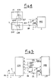
- a discriminator circuit of the power absorbed is foreseen which, in preferred example embodiments of the present invention, consists of a comparator CMP with output DO, of the open-drain type (see, in particular, figure 3).
- the signal coming from RS, mediated by the low power filter LPF, is compared with a low voltage reference LVR.
- a second comparator circuit PI ("preheat inhibit") is used to inhibit the recognition of the fluorescent lamp LF during the preheating step of the filaments.
- the output OUT of the comparator PI is low and forces to ground the low voltage reference LVR of the comparator CMP.
- the output DO (open-drain output) of the comparator CMP relative to the power signal is connected to the pin 6 (capacitor CT) of an integrated circuit which functions as a half-bridge driver circuit.
- the integrated circuit IR2156 is used as a half-bridge driver HBD.
- the output DO of the comparator CMP is also connected to the pin 4 (resistance RT) of the integrated driver circuit HBD, respectively, through a signal diode DS (usually a 1N4148 diode is used) and a resistance RSH.
- the output DO of the comparator CMP is high (circuit open), i.e. in minimum power conditions, the resistance RSH is connected in parallel to the resistance RT, unless there is a drop in potential on the diode DS. In such conditions, the capacitor CT is charged faster and the frequency of oscillation of the half-bridge is higher.
- the value of the resistance RT together with the value of CT, set the minimum value of the frequency of oscillation (and a corresponding maximum power value), whereas the value of the resistance RSH sets the frequency of oscillation relative to the minimum operating power condition.
- CMOS with output DO (open-drain) is used, indicated with CDO in figure 5.
- the comparator TS393 was used, in which the two voltage thresholds LVR (threshold of the power comparator CMP of figure 3) and HVR (threshold of "inhibit” of Figure 3) are obtained by a partition, formed by the resistances RDV1, RDV2, RDV3 of figure 5, of the supply voltage VCC of all of the integrated circuits, the typical value of which is 15.6 Volts.
- LVR and HVR are respectively connected to the non-inverting input of the power comparator CMP (pin 3 of the comparator CDO) and to the inverting input of the inhibit comparator PI (pin 6 of the comparator CDO).
- the inverting input of the power comparator CMP (pin 2 of the comparator CDO) is connected to the signal S coming from the resistance RS, mediated by the low-power filter R-C, whereas the inverting input of the inhibit comparator PI (pin 5 of the comparator CDO) is connected to the capacitor CPH (pin 7 of the driver circuit HBD of figure 5), with which the preheating time of the fluorescent lamp LF is set.
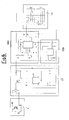
- figure 6 schematically illustrates the overall circuit of the power supply device or "ballast" object of the invention.
- said circuit has been divided into five blocks and, in particular, it is possible to identify an interference filter F ("EMI filter”), a stage S1 for the active control of the power factor (“PFC section”), a half-bridge driver circuit HBD, a discriminator circuit CDO of the power absorbed (“power comparator”) and a resonant load LR.
- EMI filter interference filter
- PFC section stage S1 for the active control of the power factor
- HBD half-bridge driver circuit
- CDO of the power absorbed power comparator
- LR resonant load
- the interference filter F is not essential for the operation of the supply circuit, but is obviously necessary to contain the interference within the limits set by the current norms in the field.
- the stage S1 allows the values of the power factor near to the unit to be obtained and allows the harmonic content of the current absorbed by the mains to be limited within the limits dictated by the norms.
- the stage S1 also allows a virtually constant continuous regulated voltage (with a low residual "ripple” at 100 Hz) to be obtained with which the half-bridge is to be supplied.
Landscapes
- Circuit Arrangements For Discharge Lamps (AREA)
Abstract
Description
- figure 1 shows a circuit diagram relative to the topology of the power stage of the power supply device, according to the present invention;
- figure 2 shows a circuit for measuring the power absorbed by each lamp, which is used in the power supply device, according to the present invention;
- figures 3 and 4 show a block diagram of a discriminator circuit of the power absorbed and a circuit for changing the frequency of oscillation, which are present in a power supply device, according to the present invention;
- figure 5 represents a circuit for comparing and varying the frequency used in the power supply device, according to the present invention;
- figure 6 shows an example overall embodiment of the electronic circuit for supplying high-frequency power for fluorescent lamps, according to the present invention.
Claims (9)
- Electronic circuit for supplying high-frequency power for fluorescent lamps (LF), characterised in that it comprises a command circuit (HBD) of a power stage, a resonant load circuit (LR) and a discriminator circuit (CDO) of the active power absorbed by each lamp (LF), which measures the power absorbed by each type of fluorescent lamp (LF), so that said lamp (LF) is correctly supplied with consequent determined values of current and voltage.
- Electronic power supply circuit according to claim 1, characterised in that it also comprises at least one interference filter (F) and at least one circuit stage (S1) for actively controlling the power factor, in order to obtain power factor values near to the unit and to limit the harmonic content of the current absorbed by the mains, said circuit control stage (S1) also allowing a substantially constant continuous regulated voltage to be obtained with which said power stage is to be supplied.
- Electronic power supply circuit according to claim 1, characterised in that said power stage is of the half-bridge type and comprises a resonant load of the series type with resonance capacitor (CRES) and inductor (LRES), said fluorescent lamp (LF) being connected in parallel to said resonance capacitor (CRES).
- Electronic power supply circuit according to claim 1, characterised in that power transistor devices (QHIGH, QLOW), which are supplied with power by a high voltage ballast (HVB), are connected to said series resonant load, said transistor devices (QHIGH, QLOW) being driven by said driver circuit (HBD) and said connection to the supply line being used to operate a preheating step of the filaments of said lamp (LF) during which said supply circuit oscillates at a predetermined frequency value, independently from the type of fluorescent lamp (LF) connected.
- Electronic power supply circuit according to claim 4, characterised in that following said preheating step of the filaments of the lamp (LF) there is a step in which said frequency of oscillation gradually reduces moving closer to the resonant frequency value of said resonant circuit (CRES, LRES), so that the voltage at the ends of said lamp (LF), increasing, allows it to be switched on.
- Electronic power supply circuit according to claim 5, characterised in that said frequency of oscillation of the half-bridge circuit is regulated so as to adapt the voltage and current values applied to said fluorescent lamp (LF), according to the average power values absorbed by the lamp (LF) with respect to a determined threshold value.
- Electronic power supply circuit according to claim 6, characterised in that one of the terminals of at least one of said power transistor devices (QLOW) is connected to at least one resistive element (RS), suitable for measuring the power absorbed by said lamp (LF), said resistive element (RS) being connected to a low-power filter (LPF) which is, in turn, connected in cascade to said discriminator circuit (CDO) of the power absorbed.
- Electronic power supply circuit according to claim 7, characterised in that said discriminator circuit (CDO) comprises at least one first comparator device (CMP) with output (DO) of the open-drain type, said first comparator (CMP) taking care of comparing a signal (S) coming from said resistive element (RS) and mediated by said low-power filter (LPF) with a low voltage reference (LVR), so as to force said output (DO) to ground or to make it an open circuit, according to the value of said signal (S) compared to said low voltage reference (LVR).
- Electronic power supply circuit according to claim 8, characterised in that a second comparator device (PI) is used to inhibit the recognition of said fluorescent lamp (LF) during the preheating step of the filaments, the output (OUT) of said second comparator (PI) being connected to said low voltage reference (LVR).
Applications Claiming Priority (2)
| Application Number | Priority Date | Filing Date | Title |
|---|---|---|---|
| ITMI20012453 | 2001-11-21 | ||
| ITMI20012453 ITMI20012453A1 (en) | 2001-11-21 | 2001-11-21 | HIGH FREQUENCY ELECTRONIC POWER CIRCUIT FOR LAMPS |
Publications (2)
| Publication Number | Publication Date |
|---|---|
| EP1315406A2 true EP1315406A2 (en) | 2003-05-28 |
| EP1315406A3 EP1315406A3 (en) | 2004-05-12 |
Family
ID=11448622
Family Applications (1)
| Application Number | Title | Priority Date | Filing Date |
|---|---|---|---|
| EP02079806A Withdrawn EP1315406A3 (en) | 2001-11-21 | 2002-11-18 | Electronic circuit for supplying high-frequency power for fluorescent lamps |
Country Status (2)
| Country | Link |
|---|---|
| EP (1) | EP1315406A3 (en) |
| IT (1) | ITMI20012453A1 (en) |
Cited By (1)
| Publication number | Priority date | Publication date | Assignee | Title |
|---|---|---|---|---|
| WO2010031535A1 (en) | 2008-09-16 | 2010-03-25 | Tridonicatco Gmbh & Co. Kg | Determination of the type of a lamp or the topology of a plurality of lamps |
Family Cites Families (5)
| Publication number | Priority date | Publication date | Assignee | Title |
|---|---|---|---|---|
| WO1980001839A1 (en) * | 1979-02-27 | 1980-09-04 | New Nippon Electric Co | Gas concentration detector |
| US4356432A (en) * | 1981-02-25 | 1982-10-26 | Exxon Research And Engineering Co. | Solid state power switch for gas discharge lamps |
| JPH0658830B2 (en) * | 1987-11-30 | 1994-08-03 | 池田電機株式会社 | Discharge lamp lighting device |
| JP3273161B2 (en) * | 1996-06-11 | 2002-04-08 | シャープ株式会社 | Load drive circuit |
| JP3694146B2 (en) * | 1997-06-10 | 2005-09-14 | 三菱電機株式会社 | Discharge lamp lighting device |
-
2001
- 2001-11-21 IT ITMI20012453 patent/ITMI20012453A1/en unknown
-
2002
- 2002-11-18 EP EP02079806A patent/EP1315406A3/en not_active Withdrawn
Cited By (1)
| Publication number | Priority date | Publication date | Assignee | Title |
|---|---|---|---|---|
| WO2010031535A1 (en) | 2008-09-16 | 2010-03-25 | Tridonicatco Gmbh & Co. Kg | Determination of the type of a lamp or the topology of a plurality of lamps |
Also Published As
| Publication number | Publication date |
|---|---|
| EP1315406A3 (en) | 2004-05-12 |
| ITMI20012453A1 (en) | 2003-05-21 |
Similar Documents
| Publication | Publication Date | Title |
|---|---|---|
| CN1147209C (en) | inverter | |
| US7129647B2 (en) | Electronic ballast with programmable processor | |
| CA2338507C (en) | Electronic ballast with frequency management | |
| KR101521834B1 (en) | Led lighting device using ballast | |
| JP3600976B2 (en) | Discharge lamp lighting device | |
| KR20000016493A (en) | Ballast | |
| US5892335A (en) | Gas discharge lamp with active crest factor correction | |
| KR20140105658A (en) | Led lighting device using ballast | |
| JP2004514250A (en) | Voltage regulated electronic ballast for multiple discharge lamps | |
| CN1197586A (en) | Power supply for powering and starting gas discharge lamps | |
| KR20000016492A (en) | Anti-flicker scheme for fluorescent lamp ballast driver | |
| JP2005533362A5 (en) | ||
| US7045967B2 (en) | Multi-lamp actuating facility | |
| US20030057866A1 (en) | Electronic ballast and lighting fixture | |
| US8593078B1 (en) | Universal dimming ballast platform | |
| KR101522694B1 (en) | Led lamp using alternative form circuit of fluorescent lamp | |
| JP2004521467A (en) | Circuit device | |
| KR100426647B1 (en) | Electronic ballast which comprising a control circuit of cathode pre-heating current therein | |
| JP4441108B2 (en) | Discharge lamp lighting device | |
| JP4314978B2 (en) | Discharge lamp lighting device and lighting fixture | |
| JP4124791B2 (en) | Electronic ballast for fluorescent lamp | |
| JP4283348B2 (en) | Discharge lamp lighting device | |
| JP3890688B2 (en) | Discharge lamp lighting device | |
| JP2007194224A (en) | Discharge lamp lighting device | |
| JPH0634396B2 (en) | Lamp abnormality detection circuit |
Legal Events
| Date | Code | Title | Description |
|---|---|---|---|
| PUAI | Public reference made under article 153(3) epc to a published international application that has entered the european phase |
Free format text: ORIGINAL CODE: 0009012 |
|
| AK | Designated contracting states |
Designated state(s): AT BE BG CH CY CZ DE DK EE ES FI FR GB GR IE IT LI LU MC NL PT SE SK TR |
|
| AX | Request for extension of the european patent |
Extension state: AL LT LV MK RO SI |
|
| PUAL | Search report despatched |
Free format text: ORIGINAL CODE: 0009013 |
|
| AK | Designated contracting states |
Kind code of ref document: A3 Designated state(s): AT BE BG CH CY CZ DE DK EE ES FI FR GB GR IE IT LI LU MC NL PT SE SK TR |
|
| AX | Request for extension of the european patent |
Extension state: AL LT LV MK RO SI |
|
| AKX | Designation fees paid | ||
| REG | Reference to a national code |
Ref country code: DE Ref legal event code: 8566 |
|
| STAA | Information on the status of an ep patent application or granted ep patent |
Free format text: STATUS: THE APPLICATION IS DEEMED TO BE WITHDRAWN |
|
| 18D | Application deemed to be withdrawn |
Effective date: 20041113 |