EP1315294A2 - Method for adjusting and stabilizing the frequency of an acoustic resonator - Google Patents
Method for adjusting and stabilizing the frequency of an acoustic resonator Download PDFInfo
- Publication number
- EP1315294A2 EP1315294A2 EP02020669A EP02020669A EP1315294A2 EP 1315294 A2 EP1315294 A2 EP 1315294A2 EP 02020669 A EP02020669 A EP 02020669A EP 02020669 A EP02020669 A EP 02020669A EP 1315294 A2 EP1315294 A2 EP 1315294A2
- Authority
- EP
- European Patent Office
- Prior art keywords
- electrode
- fbar
- resonant frequency
- oxidizing
- oxidation
- Prior art date
- Legal status (The legal status is an assumption and is not a legal conclusion. Google has not performed a legal analysis and makes no representation as to the accuracy of the status listed.)
- Granted
Links
Images



Classifications
-
- H—ELECTRICITY
- H03—ELECTRONIC CIRCUITRY
- H03H—IMPEDANCE NETWORKS, e.g. RESONANT CIRCUITS; RESONATORS
- H03H3/00—Apparatus or processes specially adapted for the manufacture of impedance networks, resonating circuits, resonators
- H03H3/007—Apparatus or processes specially adapted for the manufacture of impedance networks, resonating circuits, resonators for the manufacture of electromechanical resonators or networks
- H03H3/02—Apparatus or processes specially adapted for the manufacture of impedance networks, resonating circuits, resonators for the manufacture of electromechanical resonators or networks for the manufacture of piezoelectric or electrostrictive resonators or networks
- H03H3/04—Apparatus or processes specially adapted for the manufacture of impedance networks, resonating circuits, resonators for the manufacture of electromechanical resonators or networks for the manufacture of piezoelectric or electrostrictive resonators or networks for obtaining desired frequency or temperature coefficient
Definitions
- the invention relates generally to acoustic resonators and more particularly to adjusting and stabilizing the resonant frequency of a film bulk acoustic resonator (FBAR).
- FBAR film bulk acoustic resonator
- a common signal path is coupled to both an input of a receiver and an output of a transmitter.
- an antenna may be coupled to the receiver and the transmitter.
- a duplexer is often used to couple the common signal path to the input and the output. The function of the duplexer is to provide the necessary coupling to and from the common signal path, while preventing the signals generated by the transmitter from being coupled to the input of the receiver.
- a half duplexer uses a switch to connect the common signal path to the receiver or the transmitter on a time division basis.
- the half duplexer has the desired attenuation properties, but is unacceptable in many telephony applications, since it does not allow parties of a call to speak and be heard simultaneously.
- a type of duplexer that is more acceptable for telephony applications is the full duplexer.
- a full duplexer operates only if the transmit signal has a frequency that is different than the frequency of the receive signal.
- the full duplexer incorporates band-pass filters that isolate the transmit signal from the receive signal according to the frequencies.
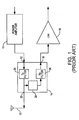
- Fig. 1 illustrates a conventional circuit used in cellular telephones, personal communication system (PCS) devices and other transmit/receive devices.
- a power amplifier 10 of a transmitter is connected to a transmit port 12 of a full duplexer 14.
- the duplexer also includes a receive port 16 that is connected to a low noise amplifier (LNA) 18 of a receiver.
- LNA low noise amplifier
- the duplexer 14 includes an antenna port 20, which is connected to an antenna 22.
- the duplexer 14 is a three-port device having the transmit port 12, the receive port 16 and the antenna port 20. Internally, the duplexer includes a transmit band-pass filter 24, a receive band-pass filter 26 and a phase shifter 28. The passbands of the two filters 24 and 26 are respectively centered on the frequency range of the transmit signal that is input via the power amplifier 10 and the receive signal to which the receiver is tuned.
- the requirements for the band-pass filters 24 and 26 of the duplexer 14 are stringent.
- the band-pass filters must isolate low intensity receive signals generated by the antenna 22 from the strong transmit signals generated by the power amplifier 10.
- the sensitivity of the low noise amplifier may be in the order of -100 dBm, while the power amplifier may provide transmit signals having an intensity of approximately 28 dBm.
- the duplexer 14 must attenuate the transmit signal by approximately 50 dB between the antenna port 20 and the receive port 16 to prevent any residual transmit signal mixed with the receive signal at the receive port from overloading the low noise amplifier.
- a passband 30 is defined by at least two of poles and at least two of zeros. The poles and zeros are equidistantly spaced from a center frequency 32.
- the transmitter-to-antenna insertion loss 34 is preferably less than -3 dB over most of the band. The isolation from the transmitter to receiver ports exceeds 50 dB across most of the transmitter band and 46 dB in the receiver band.
- the crossover between the transmitter and receiver bands occurs around 1900 MHz, which is 20 MHz below the CDMA specification.
- the lower-frequency pole is determined by the characteristics of shunt resonators, while the higher-frequency pole is determined by the characteristics of series resonators.
- the power amplifier 10 in the transmitter of Fig. 1 can deliver 1 Watt of power to the transmit port 12 of the duplexer 14.
- the band-pass filter 24 must be capable of handling such power without being destroyed and without its performance being degraded.
- the duplexer 14 of Fig. 1 will be described in greater detail with reference to Fig. 3.
- the duplexer includes a transmit film bulk acoustic resonator (FBAR) array 40 and a receive FBAR array 42.
- the transmit FBAR array 40 is a 21 ⁇ 2-stage ladder circuit having three series FBARs 44, 46 and 48 and two shunt FBARs 50 and 52.
- the series FBARs are connected in series between the transmit port 12 and the antenna port 20, while the shunt FBARs are connected between electrical ground and nodes between the series FBARs.
- Each full stage of an FBAR array is composed of one series FBAR and one shunt FBAR.
- a half stage is limited to either one series FBAR or one shunt FBAR. In the exemplary array 40, the half stage is the series FBAR 48.
- the receive FBAR array 42 is a 31 ⁇ 2-stage ladder circuit.
- the FBAR array includes three series FBARs 54, 56 and 58 and four shunt FBARs 60, 62, 64 and 66.
- the series FBARs are connected in series between the ninety degree phase shifter 28 and the receive port 16.
- the shunt FBARs are connected between electrical ground and nodes between the series FBARs.
- phase shifter 28 may be composed of inductors and capacitors or may be a ⁇ /4 transmission line.
- each series FBAR 44, 46 and 48 may have the same resonant frequency (f r ).
- the shunt FBARs 50 and 52 may have the same resonant frequency, but the resonant frequency of the series FBARs is approximately 3.0 percent greater than that of the shunt FBARs.
- the receive FBAR array 42 of the receive band-pass filter 26 may also be composed of series FBARs 54, 56 and 58 having the same f r and shunt FBARs 60, 62, 64 and 66 having the same f r that is 3.0 percent different than the resonant frequency of the series FBARs.
- the receive band-pass filter 26 is required to attenuate the transmit signal to such a low level that the residual transmit signal mixed with the receive signal at the receive port 16 does not overload the low noise amplifier 18 of Fig. 1. Consequently, the transmit signal rejection requirements of the receive band-pass filter are considerably more stringent than the receive signal rejection requirements of the transmit band-pass filter 24. This is most easily achieved if the shunt FBARs 60, 62, 64 and 66 of the receive FBAR array have more than one resonant frequency.
- the resonant frequency of the series FBARs 54, 56 and 58 of the receive FBAR array may be approximately 80 MHz higher than the resonant frequency of the series FBARs 44, 46 and 48 of the transmit FBAR array.
- the center frequencies of the two arrays will be offset.
- each FBAR in the transmit FBAR array 40 and the receive FBAR array 42 be tuned to its target frequency, so that the transmit band-pass filter 24 and the receive band-pass filter 26 can properly isolate the transmit signals from the receive signals without any objectionable crossover noise. Furthermore, optimal performance of the duplexer 14 can only be achieved if the band-pass filters 24 and 26 remain stable over an extended period of time without any frequency shift in either direction, i.e., an increase or a decrease in frequency.
- FBARs fabricated on different wafers may not produce the target resonant frequency required for optimal performance. As a result, a number of FBARs may yield resonant frequencies that are beyond the acceptable margin of error of the target resonant frequency.
- an FBAR 68 is shown as comprising of an electrode-piezoelectric stack 72 that is above a substrate 70.
- the electrode-piezoelectric stack 72 has a bottom metallic electrode layer 74 and a top metallic electrode layer 78 with a piezoelectric (PZ) layer 76 sandwiched between the two electrode layers 74 and 78.
- PZ piezoelectric
- this method requires sputtering a protective layer (e.g., aluminum) that is chemically inert to the etching process over the portions of the FBAR which are not to be etched. This extra step adds to the overall cost of FBAR fabrication.
- a protective layer e.g., aluminum
- the required FBAR performance is still achieved by adjusting their resonant frequencies to conform to the target resonant frequencies.
- the preferred method for adjusting the resonant frequency of an off-target FBAR requires intentionally oxidizing a top surface of the top metallic electrode layer at an elevated temperature for a selected period of time. The oxidization process induces a change in the molecular structure of the electrode material (e.g., Mo) from one state to another when the electrode is exposed to the oxygen. Specifically, the Mo reacts with oxygen to form molybdenum oxide.
- the electrode material e.g., Mo
- the Mo is intentionally exposed to an oxidizing environment that is gas comprising of about 20% oxygen.
- the oxidation process can be accelerated by elevating the temperature of the oxidation-inducing environment over a hot-plate or similar structure.
- the oxidizing environment is within a rapid thermal annealer (RTA) in which the temperature and the amount of oxygen entering into the oxidizing environment can easily be controlled.
- RTA rapid thermal annealer
- the Mo on the top surface of the electrode layer reacts with oxygen to form molybdenum oxide molecules.
- the molybdenum oxide molecules continue to grow on the top surface of the electrode layer, thereby increasing the thickness of the top metallic electrode layer.
- the resonant frequency can be modified by varying the total thickness of the electrode layers relative to the piezoelectric layer.
- the resonant frequency exhibited by the FBAR can be adjusted downwardly by increasing the ratio of the total thickness of the electrode layers relative to the piezoelectric layer.
- the resonant frequency exhibited for the same FBAR can be adjusted upwardly by decreasing the ratio of the total thickness of the electrode layers relative to the piezoelectric layer.
- the resonant frequency of the FBAR is adjusted downwardly.
- intentionally inducing oxidation is used as a technique for stabilizing the resonant frequency for a given FBAR.
- the number of Mo available for oxidation decreases in a logarithmic manner. For example, although it might take two hours to grow 100 angstroms of molybdenum oxide, it may take another 10 hours to grow a duplicate amount. The reason for this phenomenon is that a decline occurs in the availability of Mo for oxidation as Mo transforms into molybdenum oxides.
- the thickness of the top electrode layer approaches a finite level over an extended period as the rate of oxidation decreases. Since the resonant frequency is dependent upon the "weighted thickness" of the piezoelectric stack, the resonant frequency for an FBAR is stabilized as the thickness of the electrode approaches a steady state relative to the piezoelectric layer.
- a target resonant frequency is selected for an FBAR in step 88.
- the target resonant frequency may comply with CDMA requirements, but the invention may be used in other applications.
- the FBAR 68 may be formed on top of a substrate 70, but this is not critical. Conventionally, FBARs of the type described are formed on a silicon substrate. As shown, the FBAR 68 comprises an electrode-piezoelectric stack 72 that is above the substrate 70. The electrode-piezoelectric stack 72 has a bottom metallic electrode layer 74 and a top metallic electrode layer 78 with a piezoelectric (PZ) layer 76 sandwiched between the two electrode layers.
- the preferred material for forming the piezoelectric layer 76 is AIN, but other materials may be utilized (e.g., zinc oxide).
- the preferred electrode material for electrode layers 74 and 78 is Mo, but other metals may be substituted (e.g., aluminum, tungsten, gold or titanium).
- the resonance characteristics are dependent upon geometrical factors such as the thickness of the piezoelectric layer 76, the thicknesses of the electrodes 74 and 78, and the area of overlap between the electrodes.
- the resonant frequency is dependent upon the "weighted thickness" of the electrode-piezoelectric stack.
- the weighted thickness is the physical thickness with an adjustment that is based upon the selection of the electrode and piezoelectric materials. The adjustment is necessary, since the velocity of sound is different in different materials. Changing the weighted thickness of one or both of the electrodes changes the weighted thickness of the electrode-piezoelectric stack, thereby adjusting the resonant frequency of the stack.
- Fig. 4 shows an electrode-piezoelectric stack 72 suspended over a cavity 80 to provide resonator-to-air interfaces at both sides.
- a solidly mounted resonator (SMR) 82 of Fig. 6 is fabricated without diverging from the invention.
- the SMR 82 is shown as including an acoustic Bragg reflector 84 that is situated below the electrode-piezoelectric stack 72 and above the substrate 70 to provide a large acoustic impedance.
- the Bragg reflector 84 is made of layers of alternating high and low acoustic impedance materials, with each layer having a thickness of approximately one quarter wavelength of the resonant frequency of the SMR 82.
- an electrode-piezoelectric stack having an off-target resonant frequency is selected in step 90.
- the "selection" step is implemented by identifying an FBAR that does not meet a specification.
- the FBAR to be fabricated is unintentionally outside of the acceptable margin of error (e.g., 1%) of the target resonator frequency.
- the FBAR having an off-target resonant frequency is corrected by thermal oxidation.
- the oxidation process alters the molecular structure of the Mo that is located on the surface of the top electrode layer, forming molybdenum oxide.
- a molybdenum oxide layer 100 is formed on the surface of the top electrode layer 78 of an FBAR 98. While the layers 78 and 100 are shown as being separate layers, they are integrally linked. As a result of intentionally induced oxidation, the overall thickness of the top electrode layer (now comprising of the former electrode layer 78 and an additional molybdenum layer 100) increases.
- the resonant frequency for a given FBAR is dependent upon the "weighted thickness" of the electrode-piezoelectric stack 86, the resonant frequency can be modified by varying the total thickness of the electrode layers 78 and 74 relative to the piezoelectric layer 76. Accordingly, the resonant frequency exhibited by the FBAR 98 can be adjusted downwardly in a controlled manner.
- the thermal oxidation step 92 of Fig. 5 can be used to stabilize the resonant frequency of the FBAR 98.
- the molybdenum oxide layer 100 continues to grow on the surface of the top electrode layer 78, the number of Mo available for further oxidation decreases in a logarithmic fashion.
- the thickness of the top electrode layer approaches a finite level over an extended period as the rate of oxidation decreases.
- the resonant frequency for the FBAR 98 is stabilized as the overall thickness of the electrode layer (now comprising the electrode layer 78 and the molybdenum oxide layer 100) approaches a steady state relative to the piezoelectric layer 76.
- the thermal oxidation step 92 of Fig. 5 occurs in an oxidation-inducing environment that is air over a hot-plate.
- oxidation step 92 occurs in an oxidation-inducing environment that is within a rapid thermal annealer (RTA).
- RTA rapid thermal annealer
- FIG. 8 an RTA 102 is shown in which the temperature can be elevated by a temperature controller 104.
- the flow rates and percentages of gases, including oxygen, entering the oxidizing environment of RTA 102 can be controlled by a gas monitor controller 106.
- the temperature of the oxidization inducing environment is elevated to 215 degrees Celsius.
- the passband at the 3 dB bandwidth 112 corresponds to a left frequency 114 (i.e., f 3dB_L ) and a right frequency 116 (i.e., f 3dB_R ).
- the two frequencies 114 and 116 at which the transmission drops by 3 dB is the 3dB insertion loss 118 of the 3 dB bandwidth 112.
- the passband at the 15 dB bandwidth 120 corresponds to a left frequency 122 (i.e., f 15dB_L ) and a right frequency 124 (i.e., f 15dB_R ).
- the two frequencies 122 and 124 at which the transmission drops by 15 dB define the 15 dB insertion loss 126 of the 15 dB bandwidth 120.
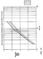
- a graph is shown in which the FBAR 98 is intentionally exposed to an oxidation environment at an elevated temperature of 215 degrees Celsius.
- the horizontal axis is the measure of time t in minutes and the vertical axis is the measure of frequency f shift down in MHz.
- Each of the plots (i.e., 122, 114, 116 and 124) in Fig. 10 represents one of the four passband frequencies 122, 114, 116 and 124 in Fig. 9.
- the FBAR is intentionally oxidated for a selected period of time t , there is a change in frequencies 122, 114, 116 and 124 as a function of time.
- the left frequency 114 and the right frequency 116 corresponding to the 3 dB bandwidth 112 are adjusted downwardly.
- the left frequency 122 and the right frequency 124 corresponding to the 15 dB bandwidth 120 are adjusted downwardly.
- oxidation time t 1.291In t - 1.5673 where the frequency f is measured in MHz and the time t is measured in minutes.
- a thermal oxidation time of 100 minutes at 215 degrees Celsius would result in a downward shift of frequencies 114, 116, 122 and 124 of approximately 4.4 MHz.
- Fig. 10 shows a strong linear correlation between an increase in time and a downward shift in frequencies 114, 116, 122 and 124.
- the coefficient r always has a value between -1 and +1, reflecting the consistency of the effect that a change in one variable has on the other.
- a value of +1 signifies a perfect positive correlation
- a value of -1 shows a perfect negative correlation.
- the coefficient of linear correlation r is approximately 0.996, which reflects a downward shift in frequency as being almost linear, given the increase in oxidation time at 215 degrees Celsius in air.
- Fig. 11 illustrates the frequency shifts measured in MHz on the vertical axis due to oxidation after eight-five minutes at 215 degrees Celsius air anneal for six sample FBARs 128, 130, 132, 134, 136 and 138 that are designated on the horizontal axis.
- the bandpass characteristics are given by (a) the left frequency 144 corresponding to the 15 dB insertion loss, (b) the left frequency 140 corresponding to the 3 dB insertion loss, (c) the right frequency 142 corresponding to the 3 dB insertion loss, and (d) the right frequency 146 corresponding to the 15 dB insertion loss.
- Fig. 11 follows the same format as Fig. 9. That is, the frequencies 144, 146, 140 and 142 of the sample FBAR 128 in Fig. 11 correspond to the respective frequencies 122, 114, 116 and 124 of the FBAR 110 in Fig. 9.
- While the invention has been described as being used in an FBAR 98 having a single piezoelectric layer 76, the invention may be extended to stacked FBARs, i.e., SBARs, without diverging from the level of skill in the art. That is, arrays of FBARs having stacked piezoelectric layers that are separated by electrode layers may be fabricated to have the target resonant frequencies, so as to achieve desired filter characteristics.
Landscapes
- Engineering & Computer Science (AREA)
- Manufacturing & Machinery (AREA)
- Piezo-Electric Or Mechanical Vibrators, Or Delay Or Filter Circuits (AREA)
Abstract
Description
Claims (11)
- A method for adjusting the resonant frequency of an acoustic resonator (68; 82; 98; 128, 130, 132, 134, 136 and 138) comprising the steps of:identifying an electrode-piezoelectric stack (72; 86) having an off-target resonant frequency, said electrode-piezoelectric stack having conductive electrode layers (74 and 78); andoxidizing at least one of said conductive electrode layers (74 and 78) of said electrode-piezoelectric stack (72; 86) so as to achieve a target resonant frequency that is dissimilar from said off-target resonant frequency, including intentionally inducing oxidation by exposing said at least one conductive electrode layer to an oxidizing environment.
- The method of claim 1 wherein said step of oxidizing includes thermally oxidizing said at least one conductive electrode layer (74 and 78) of said electrode-piezoelectric stack (72; 86) by exposing said electrode-piezoelectric stack to an oxidation-inducing environment at an elevated temperature.
- The method of claim 2 wherein said step of thermally oxidizing includes exposing a top electrode layer (78) of said conductive electrode layers (74 and 78) to said oxidation-inducing environment at said elevated temperature.
- The method of claim 3 wherein said step of thermally oxidizing indudes exposing a top surface of said top electrode layer (78) to said oxidation-inducing environment at said elevated temperature, said oxidizing being limited to a top region of said top electrode.
- The method of claim 1, 2, 3 or 4 wherein said step of oxidizing includes providing said oxidizing environment as air.
- The method of claim 1, 2, 3, 4 or 5 wherein said step of oxidizing includes forming said oxidizing environment within a rapid thermal annealer (RTA) (102).
- The method of claim 1, 2, 3, 4, 5 or 6 further comprising a step of fabricating said electrode-piezoelectric stack (72; 86) to be suspended over a cavity (80).
- The method of claim 1, 2, 3, 4, 5 or 6 further comprising a step of fabricating said electrode-piezoelectric stack (72; 86) over a Bragg reflector (84).
- A film bulk acoustic resonator (FBAR) (68; 82; 98; 128, 130, 132, 134, 136 and 138) comprising:wherein said FBAR (68; 82; 98; 128, 130, 132, 134, 136 and 138) having said portion of metal oxide has a resonant frequency that is substantially closer to a target resonant frequency than said FBAR without said portion of metal oxide.a substrate (70);a bottom electrode (74) above said substrate (70);a piezoelectric layer (76) above said bottom electrode (74); anda top electrode (78) having an upper region above said piezoelectric layer (76), said upper region including metal oxide, at least a portion of said metal oxide being realized by an elevated temperature that is higher than the ambient temperature;
- The FBAR (68; 82; 98; 128, 130, 132, 134, 136 and 138) of claim 9 wherein said top electrode (78) has a thickness that is greater than a comparable electrode without said portion of metal oxide being realized by said elevated temperature that is higher than said ambient temperature.
- The FBAR (68; 82; 98; 128, 130, 132, 134, 136 and 138) of claim 9 or 10 wherein said top and bottom electrodes (78 and 74) and said piezoelectric layer (76) form an element of an FBAR array (40 and 42).
Applications Claiming Priority (2)
| Application Number | Priority Date | Filing Date | Title |
|---|---|---|---|
| US996951 | 2001-11-27 | ||
| US09/996,951 US6710508B2 (en) | 2001-11-27 | 2001-11-27 | Method for adjusting and stabilizing the frequency of an acoustic resonator |
Publications (3)
| Publication Number | Publication Date |
|---|---|
| EP1315294A2 true EP1315294A2 (en) | 2003-05-28 |
| EP1315294A3 EP1315294A3 (en) | 2004-06-16 |
| EP1315294B1 EP1315294B1 (en) | 2009-02-18 |
Family
ID=25543465
Family Applications (1)
| Application Number | Title | Priority Date | Filing Date |
|---|---|---|---|
| EP02020669A Expired - Lifetime EP1315294B1 (en) | 2001-11-27 | 2002-09-13 | Method for adjusting and stabilizing the frequency of an acoustic resonator |
Country Status (4)
| Country | Link |
|---|---|
| US (1) | US6710508B2 (en) |
| EP (1) | EP1315294B1 (en) |
| JP (1) | JP4010545B2 (en) |
| DE (1) | DE60231181D1 (en) |
Cited By (2)
| Publication number | Priority date | Publication date | Assignee | Title |
|---|---|---|---|---|
| US7550900B2 (en) * | 2003-12-12 | 2009-06-23 | Stmicroelectronics Sa | Acoustic resonator device |
| CN111355459A (en) * | 2020-03-26 | 2020-06-30 | 中国科学院半导体研究所 | Frequency tuning method of MEMS resonator based on electrochemical corrosion |
Families Citing this family (71)
| Publication number | Priority date | Publication date | Assignee | Title |
|---|---|---|---|---|
| US7277403B2 (en) * | 2001-12-13 | 2007-10-02 | Avago Technologies Wireless Ip (Singapore) Pte Ltd | Duplexer with a differential receiver port implemented using acoustic resonator elements |
| CN100521527C (en) * | 2002-12-13 | 2009-07-29 | Nxp股份有限公司 | Electro-acoustic resonator |
| US7212789B2 (en) * | 2002-12-30 | 2007-05-01 | Motorola, Inc. | Tunable duplexer |
| US7275292B2 (en) | 2003-03-07 | 2007-10-02 | Avago Technologies Wireless Ip (Singapore) Pte. Ltd. | Method for fabricating an acoustical resonator on a substrate |
| US7356314B2 (en) * | 2003-04-17 | 2008-04-08 | Kyocera Wireless Corp. | Systems and methods for reusing a low noise amplifier in a wireless communications device |
| US6946928B2 (en) * | 2003-10-30 | 2005-09-20 | Agilent Technologies, Inc. | Thin-film acoustically-coupled transformer |
| US7332985B2 (en) * | 2003-10-30 | 2008-02-19 | Avago Technologies Wireless Ip (Singapore) Pte Ltd. | Cavity-less film bulk acoustic resonator (FBAR) devices |
| US7019605B2 (en) * | 2003-10-30 | 2006-03-28 | Larson Iii John D | Stacked bulk acoustic resonator band-pass filter with controllable pass bandwidth |
| US7362198B2 (en) * | 2003-10-30 | 2008-04-22 | Avago Technologies Wireless Ip (Singapore) Pte. Ltd | Pass bandwidth control in decoupled stacked bulk acoustic resonator devices |
| EP1528677B1 (en) | 2003-10-30 | 2006-05-10 | Agilent Technologies, Inc. | Film acoustically-coupled transformer with two reverse c-axis piezoelectric elements |
| US7161448B2 (en) * | 2004-06-14 | 2007-01-09 | Avago Technologies Wireless Ip (Singapore) Pte. Ltd. | Acoustic resonator performance enhancements using recessed region |
| US7114252B2 (en) * | 2004-06-17 | 2006-10-03 | Toko, Inc. | Large scale simultaneous circuit encapsulating apparatus |
| US7615833B2 (en) | 2004-07-13 | 2009-11-10 | Avago Technologies Wireless Ip (Singapore) Pte. Ltd. | Film bulk acoustic resonator package and method of fabricating same |
| US20060017352A1 (en) * | 2004-07-20 | 2006-01-26 | Aram Tanielian | Thin device and method of fabrication |
| US20060059269A1 (en) * | 2004-09-13 | 2006-03-16 | Chien Chen | Transparent recovery of switch device |
| US7388454B2 (en) * | 2004-10-01 | 2008-06-17 | Avago Technologies Wireless Ip Pte Ltd | Acoustic resonator performance enhancement using alternating frame structure |
| US7098758B2 (en) * | 2004-11-03 | 2006-08-29 | Avago Technologies Wireless Ip (Singapore) Pte. Ltd. | Acoustically coupled thin-film resonators having an electrode with a tapered edge |
| US8981876B2 (en) * | 2004-11-15 | 2015-03-17 | Avago Technologies General Ip (Singapore) Pte. Ltd. | Piezoelectric resonator structures and electrical filters having frame elements |
| US20060125084A1 (en) * | 2004-12-15 | 2006-06-15 | Fazzio Ronald S | Integration of micro-electro mechanical systems and active circuitry |
| US7202560B2 (en) | 2004-12-15 | 2007-04-10 | Avago Technologies Wireless Ip (Singapore) Pte. Ltd. | Wafer bonding of micro-electro mechanical systems to active circuitry |
| US7791434B2 (en) | 2004-12-22 | 2010-09-07 | Avago Technologies Wireless Ip (Singapore) Pte. Ltd. | Acoustic resonator performance enhancement using selective metal etch and having a trench in the piezoelectric |
| US7427819B2 (en) * | 2005-03-04 | 2008-09-23 | Avago Wireless Ip Pte Ltd | Film-bulk acoustic wave resonator with motion plate and method |
| US7369013B2 (en) * | 2005-04-06 | 2008-05-06 | Avago Technologies Wireless Ip Pte Ltd | Acoustic resonator performance enhancement using filled recessed region |
| US7436269B2 (en) | 2005-04-18 | 2008-10-14 | Avago Technologies Wireless Ip (Singapore) Pte. Ltd. | Acoustically coupled resonators and method of making the same |
| US7443269B2 (en) * | 2005-07-27 | 2008-10-28 | Avago Technologies General Ip (Singapore) Pte. Ltd. | Method and apparatus for selectively blocking radio frequency (RF) signals in a radio frequency (RF) switching circuit |
| US7378781B2 (en) * | 2005-09-07 | 2008-05-27 | Nokia Corporation | Acoustic wave resonator with integrated temperature control for oscillator purposes |
| US7868522B2 (en) | 2005-09-09 | 2011-01-11 | Avago Technologies Wireless Ip (Singapore) Pte. Ltd. | Adjusted frequency temperature coefficient resonator |
| US7391286B2 (en) * | 2005-10-06 | 2008-06-24 | Avago Wireless Ip Pte Ltd | Impedance matching and parasitic capacitor resonance of FBAR resonators and coupled filters |
| US7737807B2 (en) | 2005-10-18 | 2010-06-15 | Avago Technologies Wireless Ip (Singapore) Pte. Ltd. | Acoustic galvanic isolator incorporating series-connected decoupled stacked bulk acoustic resonators |
| US7675390B2 (en) * | 2005-10-18 | 2010-03-09 | Avago Technologies Wireless Ip (Singapore) Pte. Ltd. | Acoustic galvanic isolator incorporating single decoupled stacked bulk acoustic resonator |
| US7425787B2 (en) * | 2005-10-18 | 2008-09-16 | Avago Technologies Wireless Ip (Singapore) Pte. Ltd. | Acoustic galvanic isolator incorporating single insulated decoupled stacked bulk acoustic resonator with acoustically-resonant electrical insulator |
| US7423503B2 (en) * | 2005-10-18 | 2008-09-09 | Avago Technologies Wireless Ip (Singapore) Pte. Ltd. | Acoustic galvanic isolator incorporating film acoustically-coupled transformer |
| US7525398B2 (en) * | 2005-10-18 | 2009-04-28 | Avago Technologies General Ip (Singapore) Pte. Ltd. | Acoustically communicating data signals across an electrical isolation barrier |
| US7463499B2 (en) | 2005-10-31 | 2008-12-09 | Avago Technologies General Ip (Singapore) Pte Ltd. | AC-DC power converter |
| US7561009B2 (en) * | 2005-11-30 | 2009-07-14 | Avago Technologies General Ip (Singapore) Pte. Ltd. | Film bulk acoustic resonator (FBAR) devices with temperature compensation |
| US7612636B2 (en) * | 2006-01-30 | 2009-11-03 | Avago Technologies Wireless Ip (Singapore) Pte. Ltd. | Impedance transforming bulk acoustic wave baluns |
| US7746677B2 (en) * | 2006-03-09 | 2010-06-29 | Avago Technologies Wireless Ip (Singapore) Pte. Ltd. | AC-DC converter circuit and power supply |
| US20070210724A1 (en) * | 2006-03-09 | 2007-09-13 | Mark Unkrich | Power adapter and DC-DC converter having acoustic transformer |
| US7479685B2 (en) * | 2006-03-10 | 2009-01-20 | Avago Technologies General Ip (Singapore) Pte. Ltd. | Electronic device on substrate with cavity and mitigated parasitic leakage path |
| US7872945B2 (en) * | 2006-04-11 | 2011-01-18 | Xact Downhole Telemetry, Inc. | Dynamic efficiency optimization of piezoelectric actuator |
| US7629865B2 (en) | 2006-05-31 | 2009-12-08 | Avago Technologies Wireless Ip (Singapore) Pte. Ltd. | Piezoelectric resonator structures and electrical filters |
| US7508286B2 (en) * | 2006-09-28 | 2009-03-24 | Avago Technologies Wireless Ip (Singapore) Pte. Ltd. | HBAR oscillator and method of manufacture |
| US20080202239A1 (en) * | 2007-02-28 | 2008-08-28 | Fazzio R Shane | Piezoelectric acceleration sensor |
| US7791435B2 (en) * | 2007-09-28 | 2010-09-07 | Avago Technologies Wireless Ip (Singapore) Pte. Ltd. | Single stack coupled resonators having differential output |
| US7732977B2 (en) * | 2008-04-30 | 2010-06-08 | Avago Technologies Wireless Ip (Singapore) | Transceiver circuit for film bulk acoustic resonator (FBAR) transducers |
| US7855618B2 (en) * | 2008-04-30 | 2010-12-21 | Avago Technologies Wireless Ip (Singapore) Pte. Ltd. | Bulk acoustic resonator electrical impedance transformers |
| US9735338B2 (en) | 2009-01-26 | 2017-08-15 | Cymatics Laboratories Corp. | Protected resonator |
| US8030823B2 (en) | 2009-01-26 | 2011-10-04 | Resonance Semiconductor Corporation | Protected resonator |
| US8291559B2 (en) * | 2009-02-24 | 2012-10-23 | Epcos Ag | Process for adapting resonance frequency of a BAW resonator |
| US8902023B2 (en) * | 2009-06-24 | 2014-12-02 | Avago Technologies General Ip (Singapore) Pte. Ltd. | Acoustic resonator structure having an electrode with a cantilevered portion |
| US8248185B2 (en) * | 2009-06-24 | 2012-08-21 | Avago Technologies Wireless Ip (Singapore) Pte. Ltd. | Acoustic resonator structure comprising a bridge |
| US8193877B2 (en) * | 2009-11-30 | 2012-06-05 | Avago Technologies Wireless Ip (Singapore) Pte. Ltd. | Duplexer with negative phase shifting circuit |
| JP5617523B2 (en) * | 2009-12-08 | 2014-11-05 | 株式会社村田製作所 | Manufacturing method of multilayer piezoelectric thin film filter |
| US8796904B2 (en) | 2011-10-31 | 2014-08-05 | Avago Technologies General Ip (Singapore) Pte. Ltd. | Bulk acoustic resonator comprising piezoelectric layer and inverse piezoelectric layer |
| US9243316B2 (en) | 2010-01-22 | 2016-01-26 | Avago Technologies General Ip (Singapore) Pte. Ltd. | Method of fabricating piezoelectric material with selected c-axis orientation |
| US8962443B2 (en) | 2011-01-31 | 2015-02-24 | Avago Technologies General Ip (Singapore) Pte. Ltd. | Semiconductor device having an airbridge and method of fabricating the same |
| US9154112B2 (en) | 2011-02-28 | 2015-10-06 | Avago Technologies General Ip (Singapore) Pte. Ltd. | Coupled resonator filter comprising a bridge |
| US9425764B2 (en) | 2012-10-25 | 2016-08-23 | Avago Technologies General Ip (Singapore) Pte. Ltd. | Accoustic resonator having composite electrodes with integrated lateral features |
| US9136818B2 (en) | 2011-02-28 | 2015-09-15 | Avago Technologies General Ip (Singapore) Pte. Ltd. | Stacked acoustic resonator comprising a bridge |
| US9203374B2 (en) | 2011-02-28 | 2015-12-01 | Avago Technologies General Ip (Singapore) Pte. Ltd. | Film bulk acoustic resonator comprising a bridge |
| US9083302B2 (en) | 2011-02-28 | 2015-07-14 | Avago Technologies General Ip (Singapore) Pte. Ltd. | Stacked bulk acoustic resonator comprising a bridge and an acoustic reflector along a perimeter of the resonator |
| US9048812B2 (en) | 2011-02-28 | 2015-06-02 | Avago Technologies General Ip (Singapore) Pte. Ltd. | Bulk acoustic wave resonator comprising bridge formed within piezoelectric layer |
| US9148117B2 (en) | 2011-02-28 | 2015-09-29 | Avago Technologies General Ip (Singapore) Pte. Ltd. | Coupled resonator filter comprising a bridge and frame elements |
| US8575820B2 (en) | 2011-03-29 | 2013-11-05 | Avago Technologies General Ip (Singapore) Pte. Ltd. | Stacked bulk acoustic resonator |
| US9444426B2 (en) | 2012-10-25 | 2016-09-13 | Avago Technologies General Ip (Singapore) Pte. Ltd. | Accoustic resonator having integrated lateral feature and temperature compensation feature |
| US8350445B1 (en) | 2011-06-16 | 2013-01-08 | Avago Technologies Wireless Ip (Singapore) Pte. Ltd. | Bulk acoustic resonator comprising non-piezoelectric layer and bridge |
| US8922302B2 (en) | 2011-08-24 | 2014-12-30 | Avago Technologies General Ip (Singapore) Pte. Ltd. | Acoustic resonator formed on a pedestal |
| US8923794B2 (en) * | 2011-11-02 | 2014-12-30 | Triquint Semiconductor, Inc. | Temperature compensation of acoustic resonators in the electrical domain |
| US9236997B2 (en) * | 2013-09-23 | 2016-01-12 | Broadcom Corporation | Wireless transceiver with circulator-based quadrature duplexer and methods for use therewith |
| WO2018235339A1 (en) * | 2017-06-20 | 2018-12-27 | 株式会社村田製作所 | Resonator and resonance device |
| TWI721934B (en) * | 2020-10-22 | 2021-03-11 | 台灣奈米碳素股份有限公司 | Method for manufacturing film bulk acoustic resonance device having specific resonant frequency |
Family Cites Families (13)
| Publication number | Priority date | Publication date | Assignee | Title |
|---|---|---|---|---|
| CA1106960A (en) * | 1976-02-17 | 1981-08-11 | Virgil E. Bottom | Method of adjusting the frequency of a crystal resonator |
| US4320365A (en) * | 1980-11-03 | 1982-03-16 | United Technologies Corporation | Fundamental, longitudinal, thickness mode bulk wave resonator |
| US4638536A (en) * | 1986-01-17 | 1987-01-27 | The United States Of America As Represented By The Secretary Of The Army | Method of making a resonator having a desired frequency from a quartz crystal resonator plate |
| US5185589A (en) * | 1991-05-17 | 1993-02-09 | Westinghouse Electric Corp. | Microwave film bulk acoustic resonator and manifolded filter bank |
| US6051907A (en) * | 1996-10-10 | 2000-04-18 | Nokia Mobile Phones Limited | Method for performing on-wafer tuning of thin film bulk acoustic wave resonators (FBARS) |
| US6249074B1 (en) * | 1997-08-22 | 2001-06-19 | Cts Corporation | Piezoelectric resonator using sacrificial layer and method of tuning same |
| US6081171A (en) * | 1998-04-08 | 2000-06-27 | Nokia Mobile Phones Limited | Monolithic filters utilizing thin film bulk acoustic wave devices and minimum passive components for controlling the shape and width of a passband response |
| US6060818A (en) * | 1998-06-02 | 2000-05-09 | Hewlett-Packard Company | SBAR structures and method of fabrication of SBAR.FBAR film processing techniques for the manufacturing of SBAR/BAR filters |
| US6420820B1 (en) * | 2000-08-31 | 2002-07-16 | Agilent Technologies, Inc. | Acoustic wave resonator and method of operating the same to maintain resonance when subjected to temperature variations |
| US6424237B1 (en) * | 2000-12-21 | 2002-07-23 | Agilent Technologies, Inc. | Bulk acoustic resonator perimeter reflection system |
| US6483229B2 (en) * | 2001-03-05 | 2002-11-19 | Agilent Technologies, Inc. | Method of providing differential frequency adjusts in a thin film bulk acoustic resonator (FBAR) filter and apparatus embodying the method |
| US6469597B2 (en) * | 2001-03-05 | 2002-10-22 | Agilent Technologies, Inc. | Method of mass loading of thin film bulk acoustic resonators (FBAR) for creating resonators of different frequencies and apparatus embodying the method |
| US6472954B1 (en) * | 2001-04-23 | 2002-10-29 | Agilent Technologies, Inc. | Controlled effective coupling coefficients for film bulk acoustic resonators |
-
2001
- 2001-11-27 US US09/996,951 patent/US6710508B2/en not_active Expired - Lifetime
-
2002
- 2002-09-13 EP EP02020669A patent/EP1315294B1/en not_active Expired - Lifetime
- 2002-09-13 DE DE60231181T patent/DE60231181D1/en not_active Expired - Lifetime
- 2002-11-26 JP JP2002341761A patent/JP4010545B2/en not_active Expired - Fee Related
Cited By (3)
| Publication number | Priority date | Publication date | Assignee | Title |
|---|---|---|---|---|
| US7550900B2 (en) * | 2003-12-12 | 2009-06-23 | Stmicroelectronics Sa | Acoustic resonator device |
| CN111355459A (en) * | 2020-03-26 | 2020-06-30 | 中国科学院半导体研究所 | Frequency tuning method of MEMS resonator based on electrochemical corrosion |
| CN111355459B (en) * | 2020-03-26 | 2023-06-20 | 中国科学院半导体研究所 | MEMS resonator frequency trimming method based on electrochemical corrosion |
Also Published As
| Publication number | Publication date |
|---|---|
| US20030098631A1 (en) | 2003-05-29 |
| EP1315294B1 (en) | 2009-02-18 |
| EP1315294A3 (en) | 2004-06-16 |
| DE60231181D1 (en) | 2009-04-02 |
| JP4010545B2 (en) | 2007-11-21 |
| JP2003209451A (en) | 2003-07-25 |
| US6710508B2 (en) | 2004-03-23 |
Similar Documents
| Publication | Publication Date | Title |
|---|---|---|
| EP1315294B1 (en) | Method for adjusting and stabilizing the frequency of an acoustic resonator | |
| US6472954B1 (en) | Controlled effective coupling coefficients for film bulk acoustic resonators | |
| KR100743555B1 (en) | Transmitter filter arrangement for multiband mobile phone | |
| EP0750394B1 (en) | Saw coupled resonator filter and radio using such a filter | |
| JP4654220B2 (en) | Filter structure including a piezoelectric resonator | |
| CN100511998C (en) | Coupled BAW resonator based duplexers | |
| KR100809120B1 (en) | Ladder filters, radio frequency band pass filters, radio frequency receivers and / or transmitter devices | |
| US6741146B2 (en) | Filter structure comprising piezoelectric resonators | |
| US10727811B2 (en) | Effective coupling coefficients for strained single crystal epitaxial film bulk acoustic resonators | |
| US7106148B2 (en) | Branching filter and communication device | |
| EP1713179A1 (en) | Surface acoustic wave filter, and saw duplexer | |
| US11211918B2 (en) | Effective coupling coefficients for strained single crystal epitaxial film bulk acoustic resonators | |
| WO2022022438A1 (en) | Filter designing method, filter, multiplexer, and communication device | |
| US20070024397A1 (en) | Surface acoustic wave resonator, surface acoustic wave device, and communications equipment | |
| JP2005223808A (en) | Piezoelectric thin film filter, branching filter, and communication apparatus | |
| JP2002344349A (en) | Transmission and reception switching device using thin film piezoelectric resonator | |
| CN112187213B (en) | Duplexer design method and duplexer, multiplexer, communication equipment | |
| JP2005160056A (en) | Piezoelectric device, antenna duplexer, and method of manufacturing a piezoelectric resonator used therefor |
Legal Events
| Date | Code | Title | Description |
|---|---|---|---|
| PUAI | Public reference made under article 153(3) epc to a published international application that has entered the european phase |
Free format text: ORIGINAL CODE: 0009012 |
|
| AK | Designated contracting states |
Designated state(s): AT BE BG CH CY CZ DE DK EE ES FI FR GB GR IE IT LI LU MC NL PT SE SK TR |
|
| AX | Request for extension of the european patent |
Extension state: AL LT LV MK RO SI |
|
| PUAL | Search report despatched |
Free format text: ORIGINAL CODE: 0009013 |
|
| AK | Designated contracting states |
Kind code of ref document: A3 Designated state(s): AT BE BG CH CY CZ DE DK EE ES FI FR GB GR IE IT LI LU MC NL PT SE SK TR |
|
| AX | Request for extension of the european patent |
Extension state: AL LT LV MK RO SI |
|
| 17P | Request for examination filed |
Effective date: 20041006 |
|
| AKX | Designation fees paid |
Designated state(s): DE FR GB IT |
|
| RAP1 | Party data changed (applicant data changed or rights of an application transferred) |
Owner name: AVAGO TECHNOLOGIES WIRELESS IP (SINGAPORE) PTE. LT |
|
| 17Q | First examination report despatched |
Effective date: 20080310 |
|
| GRAP | Despatch of communication of intention to grant a patent |
Free format text: ORIGINAL CODE: EPIDOSNIGR1 |
|
| GRAS | Grant fee paid |
Free format text: ORIGINAL CODE: EPIDOSNIGR3 |
|
| GRAA | (expected) grant |
Free format text: ORIGINAL CODE: 0009210 |
|
| AK | Designated contracting states |
Kind code of ref document: B1 Designated state(s): DE FR GB IT |
|
| REG | Reference to a national code |
Ref country code: GB Ref legal event code: FG4D |
|
| REF | Corresponds to: |
Ref document number: 60231181 Country of ref document: DE Date of ref document: 20090402 Kind code of ref document: P |
|
| PLBE | No opposition filed within time limit |
Free format text: ORIGINAL CODE: 0009261 |
|
| STAA | Information on the status of an ep patent application or granted ep patent |
Free format text: STATUS: NO OPPOSITION FILED WITHIN TIME LIMIT |
|
| 26N | No opposition filed |
Effective date: 20091119 |
|
| GBPC | Gb: european patent ceased through non-payment of renewal fee |
Effective date: 20090913 |
|
| REG | Reference to a national code |
Ref country code: FR Ref legal event code: ST Effective date: 20100531 |
|
| PG25 | Lapsed in a contracting state [announced via postgrant information from national office to epo] |
Ref country code: FR Free format text: LAPSE BECAUSE OF NON-PAYMENT OF DUE FEES Effective date: 20090930 |
|
| PG25 | Lapsed in a contracting state [announced via postgrant information from national office to epo] |
Ref country code: GB Free format text: LAPSE BECAUSE OF NON-PAYMENT OF DUE FEES Effective date: 20090913 |
|
| PG25 | Lapsed in a contracting state [announced via postgrant information from national office to epo] |
Ref country code: IT Free format text: LAPSE BECAUSE OF FAILURE TO SUBMIT A TRANSLATION OF THE DESCRIPTION OR TO PAY THE FEE WITHIN THE PRESCRIBED TIME-LIMIT Effective date: 20090218 |
|
| REG | Reference to a national code |
Ref country code: DE Ref legal event code: R082 Ref document number: 60231181 Country of ref document: DE Representative=s name: DILG HAEUSLER SCHINDELMANN PATENTANWALTSGESELL, DE |
|
| REG | Reference to a national code |
Ref country code: DE Ref legal event code: R082 Ref document number: 60231181 Country of ref document: DE Representative=s name: DILG HAEUSLER SCHINDELMANN PATENTANWALTSGESELL, DE Effective date: 20130703 Ref country code: DE Ref legal event code: R081 Ref document number: 60231181 Country of ref document: DE Owner name: AVAGO TECHNOLOGIES GENERAL IP (SINGAPORE) PTE., SG Free format text: FORMER OWNER: AVAGO TECHNOLOGIES WIRELESS IP (SINGAPORE) PTE. LTD., SINGAPORE, SG Effective date: 20130703 |
|
| REG | Reference to a national code |
Ref country code: DE Ref legal event code: R082 Ref document number: 60231181 Country of ref document: DE Representative=s name: DILG, HAEUSLER, SCHINDELMANN PATENTANWALTSGESE, DE Ref country code: DE Ref legal event code: R082 Ref document number: 60231181 Country of ref document: DE Representative=s name: DILG HAEUSLER SCHINDELMANN PATENTANWALTSGESELL, DE Ref country code: DE Ref legal event code: R081 Ref document number: 60231181 Country of ref document: DE Owner name: AVAGO TECHNOLOGIES INTERNATIONAL SALES PTE. LI, SG Free format text: FORMER OWNER: AVAGO TECHNOLOGIES GENERAL IP (SINGAPORE) PTE. LTD., SINGAPORE, SG |
|
| PGFP | Annual fee paid to national office [announced via postgrant information from national office to epo] |
Ref country code: DE Payment date: 20190927 Year of fee payment: 18 |
|
| REG | Reference to a national code |
Ref country code: DE Ref legal event code: R119 Ref document number: 60231181 Country of ref document: DE |
|
| PG25 | Lapsed in a contracting state [announced via postgrant information from national office to epo] |
Ref country code: DE Free format text: LAPSE BECAUSE OF NON-PAYMENT OF DUE FEES Effective date: 20210401 |