EP1315187A2 - Substrate and manufacturing method thereof - Google Patents
Substrate and manufacturing method thereof Download PDFInfo
- Publication number
- EP1315187A2 EP1315187A2 EP02025945A EP02025945A EP1315187A2 EP 1315187 A2 EP1315187 A2 EP 1315187A2 EP 02025945 A EP02025945 A EP 02025945A EP 02025945 A EP02025945 A EP 02025945A EP 1315187 A2 EP1315187 A2 EP 1315187A2
- Authority
- EP
- European Patent Office
- Prior art keywords
- contact points
- fixed contact
- substrate
- lead
- movable contact
- Prior art date
- Legal status (The legal status is an assumption and is not a legal conclusion. Google has not performed a legal analysis and makes no representation as to the accuracy of the status listed.)
- Withdrawn
Links
- 239000000758 substrate Substances 0.000 title claims abstract description 57
- 238000004519 manufacturing process Methods 0.000 title claims abstract description 14
- 238000000034 method Methods 0.000 claims abstract description 13
- 239000002184 metal Substances 0.000 claims description 6
- 229910052751 metal Inorganic materials 0.000 claims description 6
- 238000000465 moulding Methods 0.000 claims description 3
- 239000011347 resin Substances 0.000 claims description 3
- 229920005989 resin Polymers 0.000 claims description 3
- 238000005520 cutting process Methods 0.000 claims description 2
- 238000003825 pressing Methods 0.000 claims description 2
- 230000005540 biological transmission Effects 0.000 description 7
- UTMWFJSRHLYRPY-UHFFFAOYSA-N 3,3',5,5'-tetrachlorobiphenyl Chemical compound ClC1=CC(Cl)=CC(C=2C=C(Cl)C=C(Cl)C=2)=C1 UTMWFJSRHLYRPY-UHFFFAOYSA-N 0.000 description 6
- 239000004952 Polyamide Substances 0.000 description 5
- 229920002647 polyamide Polymers 0.000 description 5
- 238000005476 soldering Methods 0.000 description 2
- RYGMFSIKBFXOCR-UHFFFAOYSA-N Copper Chemical compound [Cu] RYGMFSIKBFXOCR-UHFFFAOYSA-N 0.000 description 1
- 244000145845 chattering Species 0.000 description 1
- 239000011889 copper foil Substances 0.000 description 1
- 230000007935 neutral effect Effects 0.000 description 1
- 239000012811 non-conductive material Substances 0.000 description 1
- KKEYFWRCBNTPAC-UHFFFAOYSA-L terephthalate(2-) Chemical compound [O-]C(=O)C1=CC=C(C([O-])=O)C=C1 KKEYFWRCBNTPAC-UHFFFAOYSA-L 0.000 description 1
Images


Classifications
-
- H—ELECTRICITY
- H01—ELECTRIC ELEMENTS
- H01H—ELECTRIC SWITCHES; RELAYS; SELECTORS; EMERGENCY PROTECTIVE DEVICES
- H01H11/00—Apparatus or processes specially adapted for the manufacture of electric switches
- H01H11/0056—Apparatus or processes specially adapted for the manufacture of electric switches comprising a successive blank-stamping, insert-moulding and severing operation
-
- H—ELECTRICITY
- H01—ELECTRIC ELEMENTS
- H01H—ELECTRIC SWITCHES; RELAYS; SELECTORS; EMERGENCY PROTECTIVE DEVICES
- H01H1/00—Contacts
- H01H1/58—Electric connections to or between contacts; Terminals
- H01H1/5866—Electric connections to or between contacts; Terminals characterised by the use of a plug and socket connector
-
- H—ELECTRICITY
- H01—ELECTRIC ELEMENTS
- H01H—ELECTRIC SWITCHES; RELAYS; SELECTORS; EMERGENCY PROTECTIVE DEVICES
- H01H19/00—Switches operated by an operating part which is rotatable about a longitudinal axis thereof and which is acted upon directly by a solid body external to the switch, e.g. by a hand
- H01H19/54—Switches operated by an operating part which is rotatable about a longitudinal axis thereof and which is acted upon directly by a solid body external to the switch, e.g. by a hand the operating part having at least five or an unspecified number of operative positions
- H01H19/56—Angularly-movable actuating part carrying contacts, e.g. drum switch
- H01H19/58—Angularly-movable actuating part carrying contacts, e.g. drum switch having only axial contact pressure, e.g. disc switch, wafer switch
-
- H—ELECTRICITY
- H01—ELECTRIC ELEMENTS
- H01H—ELECTRIC SWITCHES; RELAYS; SELECTORS; EMERGENCY PROTECTIVE DEVICES
- H01H2300/00—Orthogonal indexing scheme relating to electric switches, relays, selectors or emergency protective devices covered by H01H
- H01H2300/02—Application transmission, e.g. for sensing the position of a gear selector or automatic transmission
Definitions
- the present invention relates to a substrate and a method for manufacturing the substrate. More specifically, the present invention pertains to a substrate for a slide switch that has fixed contact points and movable contact points, which slide along the fixed contact points to switch the connection state with the fixed contact points, and to a method for manufacturing the substrate.
- a slide switch is used as, for example, a shift position switch for detecting the position of a shift lever.
- Fig. 8 shows a conventional substrate for a shift position switch, which is a printed circuit board (PCB) 80.
- the PCB 80 has a substantially arcuate insulated substrate 86.
- Five fixed contact points 82 which are made of copper foil, are located on the surface of the insulated substrate 86. As shown in Fig. 9, each fixed contact point 82 projects from the surface of the insulated substrate 86. In this example, the thickness of each fixed contact point 82 is 35 ⁇ m.
- Five connecting portions 81 are located at the center of the outer circumference of the insulated substrate 86. Each connecting portion 81 is electrically connected to one of the fixed contact points 82.
- a terminal 85 is connected to each connecting portion 81 by soldering.
- the terminals 85 are connected to a controller (not shown), which controls an automatic transmission and an indicator.
- the terminals 85 are supported by a housing 84, which accommodates the
- leaf springs which are five movable contact points 83 (see Fig. 8), are rotated about the center C while sliding along the surface of the PCB 80.
- the movable contact points 83 contact all or some of the fixed contact points 82 in accordance with the position of the shift lever.
- the shift position switch sends signals corresponding to the fixed contact points 82 to which the movable contact points 83 contact to the controller via the terminals 85.
- the controller controls the operation of the automatic transmission and the indicator by determining the position of the shift lever based on the output signals.
- each fixed contact point 82 needs to be secured to one of the terminals 85 at the corresponding connecting portion 81 by soldering, the processes for manufacturing the PCB 80 are increased.
- the fixed contact points 82 are easily worn out. This is because since the fixed contact points 82 project from the surface of the insulated substrate 86, the movable contact points 83 hit the edges Y of the fixed contact points 82 when sliding along the surface of the PCB 80. Wear of the fixed contact points 82 causes improper contact between the fixed contact points 82 and the movable contact points 83 such as chattering. In addition, as shown in Fig. 9, when each movable contact point 83 moves from the insulated substrate 86 to one of the fixed contact points 82, a portion of the movable contact point 83 other than the actual contact point X contacts the edge Y of the fixed contact point 82.
- the distance S between the actual contact point X of the movable contact point 83 and the edge Y of the fixed contact point 82 needs to be always taken into consideration when designing the PCB 80.
- the edges Y of the fixed contact points 82 may be chamfered by a buffed finish. However, this increases the manufacturing cost and is thus impractical.
- the present invention provides a substrate for a slide switch.
- the slide switch has a plurality of fixed contact points and a movable contact point, which slides along the fixed contact points to switch the connection state with the fixed contact points.
- the substrate includes the fixed contact points and a plurality of terminals, each of which is electrically connected to one of the fixed contact points.
- the substrate is characterized in that each of the fixed contact points and the corresponding terminal are integrally formed.
- the present invention also provides a method for manufacturing the substrate according to claim 1.
- the method includes: forming a lead frame by pressing a metal plate, wherein the lead frame includes a plurality of lead pieces and a plurality of tie bars, which connect the lead pieces with each other, and wherein each lead piece includes a portion corresponding to the fixed contact points and a portion corresponding to the terminals; insert molding a molded body by filling a mold, in which the lead frame is set, with nonconductive resin; and cutting the tie bars by forming through holes at portions of the molded body corresponding to the tie bars.
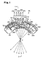
- a substrate 25 according to a preferred embodiment of the present invention will now be described with reference to Figs. 1 to 7.
- the substrate 25 is used for a shift position switch 15.
- the shift position switch 15 is arranged in a shift apparatus 11, which is located on a floor console of a vehicle.
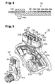
- the shift apparatus 11 includes a shift lever 12, a housing 13, a lid 14, and the shift position switch 15.
- the top of the housing 13 is open and is closed by the lid 14.
- the lid 14 has a shift gate 14a, which extends straight.
- the shift lever 12 projects upward from the shift gate 14a and is shifted along the shift gate 14a.
- Indications representing the shift position of the shift lever 12 are shown next to the shift gate 14a.
- the indications include a parking (P) range, a reverse (R) range, a neutral (N) range, a drive (D) range, a third (3rd) range, a second (2nd) range, and a low (L) range.
- a rotary shaft 17 is supported by the proximal end of the shift lever 12.
- the rotary shaft 17 extends in a direction perpendicular to the axis of the shift lever 12 and to the longitudinal direction of the shift gate 14a.
- the rotary shaft 17 is rotated about its own axis.
- the shift position switch 15 is supported by one end of the rotary shaft 17 and the inner wall of the housing 13.
- a controller 18 is electrically connected to the shift position switch 15.
- the controller 18 controls the operations of a transmission 19 and an indicator 20 based on output signals from the shift position switch 15.
- the indicator is located on, for example, an instrument panel inside the vehicle compartment and indicates the currently selected shift range.
- the shift position switch 15 will be described below. As shown in Fig. 3, the shift position switch 15 includes a stator 21 and a rotor 22.
- the stator 21 is substantially sectorial and is secured to the inner wall of the housing 13.
- a recess 21a having substantially the same sectorial shape as the stator 21 is formed in the stator 21.
- the substrate 25 is accommodated at the upper portion of the recess 21a.
- First connector terminals 23a to 23e extend from the substrate 25.
- the first connector terminals 23a to 23e are collected in an accommodating portion 24 located at the upper portion of the stator 21.
- Terminals 27 are located at a portion of the recess 21a lower than the substrate 25.
- Four second connector terminals 23f to 23i extend from the terminal 27.
- the second connector terminals 23f to 23i are also collected in the accommodating portion 24.
- An insert hole 21b is formed at the lower portion of the stator 21.
- the rotor 22 is coupled to the rotary shaft 17 to rotate integrally with the rotary shaft 17.
- the rotor 22 has a shaft 31, which is coaxial with the rotary shaft 17 and has a first end 31a and a second end 31b. The outer circumferential surface of the first end 31a is threaded. The second end 31b is rotatably inserted in the insert hole 21b.
- the rotor 22 has five leaf springs 32 (only four is shown in Fig. 3), which are located in a direction perpendicular to the axis of the shaft 31.
- the distal end of each leaf spring 32 is branched into two and curved to describe an arc (see Figs. 5(a) and 5(b)).
- the distal end of each leaf spring 32 serves as a movable contact point 32a.
- the movable contact points 32a slide along the surface of the substrate 25 when the rotor 22 is rotated.
- the substrate 25 has a substantially arcuate shape.
- the substrate 25 has five fixed contact points 28a to 28e, which are electrically connected to the first connector terminals 23a to 23e, respectively.
- the fixed contact points 28a to 28e are adhered to the insulated substrate 29 made of polyamide. Portions of the fixed contact points 28a to 28e where the movable contact points 32a contact are flush with portions of the insulated substrate 29 where the movable contact points 32a moves along.
- the fixed contact points 28a to 28e are thinner than the first connector terminals 23a to 23e.
- the thicknesses of the first connector terminals 23a to 23e are approximately 0.64mm and the thicknesses of the fixed contact points 28a to 28e are approximately 0.3mm.
- a projection 29a is located at the rear of the substrate 25 and fits in a hollow (not shown) formed in the recess 21a.
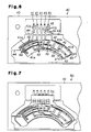
- Fig. 6 shows a lead frame 40 used for manufacturing the substrate 25.
- the lead frame 40 includes five lead pieces 41.
- Each lead piece 41 includes an inner lead portion 41a, which corresponds to one of the fixed contact points 28a to 28e, and an outer lead portion 41b, which corresponds to one of the first connector terminals 23a to 23e.
- Each outer lead portion 41b extends from the end of the corresponding inner lead portion 41a.
- the lead pieces 41 are connected to each other by first tie bars 42.
- the lead pieces 41 are connected to the frame 43, which surrounds the lead pieces 41 by second tie bars 44.
- a metal plate is pressed to form the lead frame 40.
- the metal plate has a portion that corresponds to the inner lead portions 41a and a portion that corresponds to the outer lead portion 41b.
- the portion of the metal plate that corresponds to the inner lead portions 41a is thinner than the portion of the metal plate that corresponds to the outer lead portions 41b.
- a molded body 50 as shown in Fig. 7 is formed by an insert molding. More specifically, the lead frame 40 is set in a mold, which is not shown, and molten polyamide is filled in the mold. The mold is opened after the polyamide is hardened to obtain the molded body 50, which has the lead frame 40 partially sealed by a hardened polyamide 51. When the molded body 50 is insert molded, parts of the molded body 50 corresponding to the paths of the movable contact points 32a are made flat.
- through holes 52 are formed at portions of the molded body 50 corresponding to the first tie bars 42 to cut the first tie bars 42.
- the second tie bars 44 are also cut to remove the frame 43.
- the substrate 25 as shown in Fig. 1 is obtained.
- the shift position switch 15 sends signals corresponding to the fixed contact points 28a to 28e to which the movable contact points 32a contact to the controller 18 via the first connector terminals 23a to 23e.
- the controller 18 controls the operations of the transmission 19 and the indicator 20 by determining the shift position of the shift lever 12 based on the output signals.
- the inner lead portions 41a, which correspond to the fixed contact points 28a to 28e, and the outer lead portions 41b, which correspond to the first connector terminals 23a to 23e, are manufactured using the lead frame 40, which is integrally formed in advance. Therefore, processes to connect each one of the fixed contact points 28a to 28e to the corresponding one of the first connector terminals 23a to 23e are unnecessary. This reduces the number of manufacturing processes of the substrate 25.
- the portions of the fixed contact points 28a to 28e to which the movable contact points 32a contact are flush with the portions of the insulated substrate 29 that correspond to the paths of the movable contact points 32a. This reduces wear of the fixed contact points 28a to 28e caused when the movable contact points 32a slide between the position where the movable contact points 32a contact the insulated substrate 29 (see Fig. 5(a))and the position where the movable contact points 32a contact the fixed contact points 28a to 28e (see Fig. 5(b)). Thus, improper contact between the movable contact points 32a and the fixed contact points 28a to 28e due to wear of the fixed contact points 28a to 28e is reduced. Also, it is not required to take into consideration that portions of the movable contact points 32a other than the actual contact points X contact the fixed contact points 28a to 28e when designing the substrate 25.
- the fixed contact points 28a to 28e are thinner than the first connector terminals 23a Lo 23e. Therefore, the cost is reduced as compared to a case in which the fixed contact points 28a to 28e have the same thicknesses as the first connector terminals 23a to 23e.
- the shift position switch 15 is located inside the shift apparatus 11.
- the shift position switch 15 may be located at other position of the vehicle such as the transmission 19.
- the number of the fixed contact points 28a to 28e may be four or less, or six or more.
- the number of the first connector terminals 23a to 23e may also be four or less, or six or more.
- the number of the movable contact points 32a may also be four or less, or six or more.
- the insulated substrate 29 may be formed of nonconductive material other than polyamide such as pulybutylene terephthalate.
- the shift apparatus 11 need not be located on the floor console.
- the shift apparatus 11 may be located on an instrument panel or a steering column.
- the substrate 25 may be used for slide switches other than the shift position switch 15.
Landscapes
- Engineering & Computer Science (AREA)
- Manufacturing & Machinery (AREA)
- Manufacture Of Switches (AREA)
- Rotary Switch, Piano Key Switch, And Lever Switch (AREA)
- Slide Switches (AREA)
Abstract
Description
Claims (8)
- A substrate for a slide switch (15), wherein the slide (15) switch has a plurality of fixed contact points (28a to 28e) and a movable contact point (32a), which slides along the fixed contact points (28a to 28e) to switch the connection state with the fixed contact points (28a to 28e), and wherein the substrate includes the fixed contact points (28a to 28e) and a plurality of terminals (23a to 23e), each of which is electrically connected to one of the fixed contact points (28a to 28e), the substrate being characterized in that,
each of the fixed contact points (28a to 28e) and the corresponding terminal (23a to 23e) are integrally formed. - The substrate according to claim 1, characterized in that the thickness of each fixed contact point (28a to 28e) differs from the thickness of the corresponding terminal (23a to 23e).
- The substrate according to claim 2, characterized in that each fixed contact point (28a to 28e) is thinner than the corresponding terminal (23a to 23e).
- The substrate according to any one of claims 1 to 3, characterized by an insulated substrate (29) to which the fixed contact points (28a to 28e) are adhered,
wherein a portion of each fixed contact point (28a to 28e) where the movable contact point (32a) contact is flush with a portion of the insulated substrate (29) that corresponds to a path of the movable contact point (32a). - A method for manufacturing the substrate according to claim 1, the method being characterized by:wherein the lead frame (40) includes a plurality of lead pieces (41) and a plurality of tie bars (42), which connect the lead pieces (41) with each other, and wherein each lead piece (41) includes a portion (41a) corresponding to the fixed contact points (28a to 28e) and a portion (41b) corresponding to the terminals (23a to 23e);forming a lead frame (40) by pressing a metal plate,
insert molding a molded body (50) by filling a mold, in which the lead frame (40) is set, with nonconductive resin; and
cutting the tie bars (42) by forming through holes (52) at portions of the molded body (50) corresponding to the tie bars (42). - The method according to claim 5, characterized in that the lead frame (40) is formed such that the thickness of the portion (41a) of each lead piece (41) corresponding to one of the fixed contact points (28a to 28e) differs from the thickness of the portion (41b) of each lead piece (41) corresponding to one of the terminals (23a to 23e).
- The method according to claim 6, characterized in that the lead frame (40) is formed such that the portion (41a) of each lead piece (41) corresponding to one of the fixed contact points (28a to 28e) is thinner than the portion (41b) of the lead piece (41) corresponding to one of the terminals (23a to 23e).
- The method according to any one of claims 5 to 7, characterized in that the molded body (50) is insert molded such that a portion of the molded body (50) corresponding to a path of the movable contact point (32a) is flat.
Applications Claiming Priority (2)
| Application Number | Priority Date | Filing Date | Title |
|---|---|---|---|
| JP2001355550 | 2001-11-21 | ||
| JP2001355550A JP2003157744A (en) | 2001-11-21 | 2001-11-21 | Switch substrate and its manufacturing method |
Publications (2)
| Publication Number | Publication Date |
|---|---|
| EP1315187A2 true EP1315187A2 (en) | 2003-05-28 |
| EP1315187A3 EP1315187A3 (en) | 2005-03-16 |
Family
ID=19167232
Family Applications (1)
| Application Number | Title | Priority Date | Filing Date |
|---|---|---|---|
| EP02025945A Withdrawn EP1315187A3 (en) | 2001-11-21 | 2002-11-20 | Substrate and manufacturing method thereof |
Country Status (2)
| Country | Link |
|---|---|
| EP (1) | EP1315187A3 (en) |
| JP (1) | JP2003157744A (en) |
Cited By (1)
| Publication number | Priority date | Publication date | Assignee | Title |
|---|---|---|---|---|
| CN103578835A (en) * | 2012-07-20 | 2014-02-12 | 松下电器产业株式会社 | Contact panel, control switch used for automatic transmission using the contact panel, and manufacturing methods thereof |
Families Citing this family (1)
| Publication number | Priority date | Publication date | Assignee | Title |
|---|---|---|---|---|
| JP4527142B2 (en) * | 2007-10-11 | 2010-08-18 | 朝日電装株式会社 | Inhibitor switch and manufacturing method thereof |
Family Cites Families (3)
| Publication number | Priority date | Publication date | Assignee | Title |
|---|---|---|---|---|
| DE2014496B2 (en) * | 1970-03-25 | 1972-04-06 | Siemens AG, 1000 Berlin u. 8000 München | SWITCH UNIT FOR MINIATURE ROTARY SWITCH |
| JPS5033763U (en) * | 1973-07-23 | 1975-04-11 | ||
| JP3675956B2 (en) * | 1996-06-13 | 2005-07-27 | ナイルス株式会社 | Control switch for automatic transmission and manufacturing method thereof |
-
2001
- 2001-11-21 JP JP2001355550A patent/JP2003157744A/en active Pending
-
2002
- 2002-11-20 EP EP02025945A patent/EP1315187A3/en not_active Withdrawn
Cited By (2)
| Publication number | Priority date | Publication date | Assignee | Title |
|---|---|---|---|---|
| CN103578835A (en) * | 2012-07-20 | 2014-02-12 | 松下电器产业株式会社 | Contact panel, control switch used for automatic transmission using the contact panel, and manufacturing methods thereof |
| CN103578835B (en) * | 2012-07-20 | 2017-04-26 | 松下知识产权经营株式会社 | Contact panel and control switch used for automatic transmission using the contact panel |
Also Published As
| Publication number | Publication date |
|---|---|
| EP1315187A3 (en) | 2005-03-16 |
| JP2003157744A (en) | 2003-05-30 |
Similar Documents
| Publication | Publication Date | Title |
|---|---|---|
| US7943870B2 (en) | Switch device | |
| US5967300A (en) | Switch with flexible conductor foil | |
| EP1148524B1 (en) | Seesaw-type power-supply switch device | |
| US7569782B2 (en) | Multistage switch | |
| KR19980023941A (en) | Complex operation type electric parts | |
| US20050006210A1 (en) | Switch device | |
| KR101571454B1 (en) | Electronic shift lever | |
| US7135646B2 (en) | Electrical switch | |
| JP4527142B2 (en) | Inhibitor switch and manufacturing method thereof | |
| JP3734353B2 (en) | Operation mechanism of rotating electrical parts | |
| JP2011210452A (en) | Rotary switch | |
| JPH03183338A (en) | Manufacture of wiring of motor acuator | |
| US5949041A (en) | Automatic transmission control switch and harness assembly and method of manufacture | |
| JP2009123642A (en) | Vehicle switch | |
| JP4969343B2 (en) | Speed change operation device for vehicle | |
| JP2013045503A (en) | Input device | |
| JP2621996B2 (en) | Manufacturing method of control switch for automatic transmission | |
| JP2003157744A (en) | Switch substrate and its manufacturing method | |
| WO1998014973A1 (en) | Electrical switch | |
| KR100220332B1 (en) | Composite operation electric switch | |
| JPH08227630A (en) | Manufacture of sliding contact electronic part | |
| US6995650B2 (en) | Electrical part prevented from improper mounting on circuit board, and mounting structure for the electrical part | |
| JP2011054311A (en) | Rotary switch | |
| KR100506402B1 (en) | Variable capacitor and manufacturing method thereof | |
| JP2007035402A (en) | Operation mechanism of electric device |
Legal Events
| Date | Code | Title | Description |
|---|---|---|---|
| PUAI | Public reference made under article 153(3) epc to a published international application that has entered the european phase |
Free format text: ORIGINAL CODE: 0009012 |
|
| AK | Designated contracting states |
Designated state(s): AT BE BG CH CY CZ DE DK EE ES FI FR GB GR IE IT LI LU MC NL PT SE SK TR |
|
| AX | Request for extension of the european patent |
Extension state: AL LT LV MK RO SI |
|
| PUAL | Search report despatched |
Free format text: ORIGINAL CODE: 0009013 |
|
| AK | Designated contracting states |
Kind code of ref document: A3 Designated state(s): AT BE BG CH CY CZ DE DK EE ES FI FR GB GR IE IT LI LU MC NL PT SE SK TR |
|
| AX | Request for extension of the european patent |
Extension state: AL LT LV MK RO SI |
|
| STAA | Information on the status of an ep patent application or granted ep patent |
Free format text: STATUS: THE APPLICATION IS DEEMED TO BE WITHDRAWN |
|
| AKX | Designation fees paid | ||
| 18D | Application deemed to be withdrawn |
Effective date: 20050202 |
|
| REG | Reference to a national code |
Ref country code: DE Ref legal event code: 8566 |