EP1313063A2 - Combination contact/contactless IC card - Google Patents
Combination contact/contactless IC card Download PDFInfo
- Publication number
- EP1313063A2 EP1313063A2 EP02023675A EP02023675A EP1313063A2 EP 1313063 A2 EP1313063 A2 EP 1313063A2 EP 02023675 A EP02023675 A EP 02023675A EP 02023675 A EP02023675 A EP 02023675A EP 1313063 A2 EP1313063 A2 EP 1313063A2
- Authority
- EP
- European Patent Office
- Prior art keywords
- data
- wireless
- contact
- writer
- encoded
- Prior art date
- Legal status (The legal status is an assumption and is not a legal conclusion. Google has not performed a legal analysis and makes no representation as to the accuracy of the status listed.)
- Withdrawn
Links
Images



Classifications
-
- G—PHYSICS
- G06—COMPUTING OR CALCULATING; COUNTING
- G06K—GRAPHICAL DATA READING; PRESENTATION OF DATA; RECORD CARRIERS; HANDLING RECORD CARRIERS
- G06K19/00—Record carriers for use with machines and with at least a part designed to carry digital markings
- G06K19/06—Record carriers for use with machines and with at least a part designed to carry digital markings characterised by the kind of the digital marking, e.g. shape, nature, code
- G06K19/067—Record carriers with conductive marks, printed circuits or semiconductor circuit elements, e.g. credit or identity cards also with resonating or responding marks without active components
- G06K19/07—Record carriers with conductive marks, printed circuits or semiconductor circuit elements, e.g. credit or identity cards also with resonating or responding marks without active components with integrated circuit chips
- G06K19/077—Constructional details, e.g. mounting of circuits in the carrier
- G06K19/07749—Constructional details, e.g. mounting of circuits in the carrier the record carrier being capable of non-contact communication, e.g. constructional details of the antenna of a non-contact smart card
- G06K19/07766—Constructional details, e.g. mounting of circuits in the carrier the record carrier being capable of non-contact communication, e.g. constructional details of the antenna of a non-contact smart card comprising at least a second communication arrangement in addition to a first non-contact communication arrangement
- G06K19/07769—Constructional details, e.g. mounting of circuits in the carrier the record carrier being capable of non-contact communication, e.g. constructional details of the antenna of a non-contact smart card comprising at least a second communication arrangement in addition to a first non-contact communication arrangement the further communication means being a galvanic interface, e.g. hybrid or mixed smart cards having a contact and a non-contact interface
-
- G—PHYSICS
- G06—COMPUTING OR CALCULATING; COUNTING
- G06K—GRAPHICAL DATA READING; PRESENTATION OF DATA; RECORD CARRIERS; HANDLING RECORD CARRIERS
- G06K19/00—Record carriers for use with machines and with at least a part designed to carry digital markings
- G06K19/06—Record carriers for use with machines and with at least a part designed to carry digital markings characterised by the kind of the digital marking, e.g. shape, nature, code
- G06K19/067—Record carriers with conductive marks, printed circuits or semiconductor circuit elements, e.g. credit or identity cards also with resonating or responding marks without active components
- G06K19/07—Record carriers with conductive marks, printed circuits or semiconductor circuit elements, e.g. credit or identity cards also with resonating or responding marks without active components with integrated circuit chips
-
- G—PHYSICS
- G06—COMPUTING OR CALCULATING; COUNTING
- G06K—GRAPHICAL DATA READING; PRESENTATION OF DATA; RECORD CARRIERS; HANDLING RECORD CARRIERS
- G06K19/00—Record carriers for use with machines and with at least a part designed to carry digital markings
- G06K19/06—Record carriers for use with machines and with at least a part designed to carry digital markings characterised by the kind of the digital marking, e.g. shape, nature, code
- G06K19/067—Record carriers with conductive marks, printed circuits or semiconductor circuit elements, e.g. credit or identity cards also with resonating or responding marks without active components
- G06K19/07—Record carriers with conductive marks, printed circuits or semiconductor circuit elements, e.g. credit or identity cards also with resonating or responding marks without active components with integrated circuit chips
- G06K19/0723—Record carriers with conductive marks, printed circuits or semiconductor circuit elements, e.g. credit or identity cards also with resonating or responding marks without active components with integrated circuit chips the record carrier comprising an arrangement for non-contact communication, e.g. wireless communication circuits on transponder cards, non-contact smart cards or RFIDs
Definitions
- This invention relate to a semiconductor integrated circuit, memory card, for example combination of contact type and wireless type, having the semiconductor circuit and method of using the memory card.
- Integrated circuit (IC) cards contact IC cards and wireless IC cards (wireless IC cards) are conventionally known. Because contact IC cards do not operate until being inserted into a reader/writer, a high security level can be expected. However, since contact IC cards need to be inserted into a reader/writer, there are drawbacks in that using contact IC cards is troublesome and total time required for processing is long. Meanwhile, wireless IC cards enable communications only by being brought proximity to a reader/writer, thus having an advantage in that the total time required for processing can be shortened. However, wireless IC cards also have drawbacks in that, when wireless IC cards are brought close to a reader/writer, communications are inevitably carried out, whether or not desired. Consequently, a combination card has been recently developed, in which functions of both of the above described IC cards, that is, a contact mode and a wireless frequency (hereinafter referred to as wireless) mode are mounted on a single card.
- wireless wireless frequency
- An object of the present invention is to provide a combination card and a method of using the same, the combination card enabling separate usages of communication systems thereof according to importance of security, importance of shortening of communication processing time, importance of easy communication actions, frequency of the communication actions and the like.
- another object of the present invention is to provide an LSI for a combination card, a combination card and a method of using the combination card.
- the LSI for a combination card enables communications by using both of the contact mode and the RADIO mode, encryption of transmitted/received data and communications of a high security level.
- a semiconductor integrated circuit includes: a first interface circuit to output a low-level contact mode signal when no power supply voltage is supplied, and to output a high-level contact mode signal when a power supply voltage is supplied; a second interface circuit to output a low-level wireless mode signal when no power supply voltage is supplied, and to output a high-level wireless mode signal when a power supply voltage is supplied; a switching circuit to switch a communication mode to a contact mode in the case of the high-level contact mode signal and the low-level wireless mode detecting signal, and to switch the communication mode to a wireless mode in the case of the low-level contact mode signal and the high-level wireless mode signal; a CPU to execute a processing program of the wireless mode in the wireless mode and to execute a processing program of the contact mode in the contact mode, according to the communication mode of the switching circuit; a memory circuit to store predetermined data; and an encoder circuit to encode the predetermined data held in the memory according to the wireless mode or the contact mode of the switching circuit.
- Fig. 1 is block diagram of a combination card 1 according to a first embodiment of the present invention.
- the combination card is a combination memory card including both a contact type circuit and a wireless type circuit.
- contact terminal 2 on combination card 1 of the present invention, contact terminal 2, a wireless antenna terminal 3 and LSI (semiconductor integrated circuit) 4 are mounted.
- Wireless antenna terminal 3 comprises coil. The coil can be placed any place in card 1, for example, surrounding wireless antenna terminal 3 or peripheral portion of the card 1. In this embodiment, the coil is mounted in wireless antenna terminal 3.
- contact terminal 2 includes a number of external terminals (electrodes), such as a clock (CLOCK) terminal, a reset (RESET) terminal, a power source (VDD) terminal, a ground (GND) terminal and an input/output (I/O) terminal.
- Contact terminal 2 permites transmission/reception of various types of data SC and power supply voltage VC by contacting those external terminals directly with a contact reader/writer 20.
- Wireless antenna terminal 3 is for executing transmission/reception of data with wireless reader/writer 21, and for obtaining signal SR from wireless reader/writer 21 and converting to power supply voltage VR.
- Fig. 2 shows an internal arrangement of semiconductor chip 4, shown in Fig.1, for a combination card according to a first embodiment of the present invention.
- semiconductor chip 4 includes a contact-type interface 15 for inputting/outputting various data, which is connected to the contact terminal 2; a wireless interface 16 for inputting/outputting various data, which is connected to wireless antenna terminal 3; a switching circuit 17 for switching communication modes, which is connected to contact interface 15 and wireless interface 16; a central processing unit (CPU) 11; a decoder circuit 18; and an encoder circuit 19.
- CPU central processing unit
- Power voltage supply is depending on standardized system in which contact reader/writer 20 is included. In general, power voltage supply is, for example, 5V, 3V or 1.8V.
- the contact interface 15 is connected to respective terminal pads (bonding pads) such as a clock (CLOCK) terminal pad, a reset (RESET) terminal pad, a power source (VDD) terminal pad, a ground (GND) terminal pad and an input/output (I/O) terminal pad.
- terminal pads such as a clock (CLOCK) terminal pad, a reset (RESET) terminal pad, a power source (VDD) terminal pad, a ground (GND) terminal pad and an input/output (I/O) terminal pad.
- the contact interface 15 permits transmission/reception of various data and signals to/from an external device (reader/writer) and a power source supplies to LSI 4.
- Wireless reader/writer 21 send wireless signal, then wireless antenna 3 convert the wireless signal to voltage. We use the voltage as power supply voltage VR for wireless interface circuit 16.
- a wireless wave signal (AC signal) for power source which is received via wireless antenna terminal 3
- AC signal a wireless wave signal
- DC power a power source potential
- the switching circuit 17 performs switching between the wireless mode and the contact mode in accordance with the contact mode detecting signal (VC) and the wireless mode detecting signal (VR) which are output from the contact interface 15 and wireless interface 16 respectively.
- the communication mode is switched to the contact mode.
- the communication mode is switched to the wireless mode.
- the wireless mode transmission and reception of data is performed between the wireless interface 16 and the CPU 11.
- the contact mode transmission and reception of data is performed between the contact interface 15 and the CPU 11.
- the CPU 11 is a processing unit for processing various signals and executes processing programs according to the communications mode of the switching circuit 17.
- a processing program for the wireless mode which is stored in a ROM 12, is executed; meanwhile, in the case of the contact mode, a processing program for the contact mode, which is stored in the ROM 12, is executed.
- the CPU 11 also includes control means for controlling inputs and outputs of the ROM 12, a RAM 13, an EEPROM 14, the decoder circuit 18, the encoder circuit 19 respectively.
- the decoder circuit 18 is a circuit for decoding various encoded data.
- the encoder circuit 19 is a circuit for encoding various data such as ID data in accordance with the wireless mode of the switching circuit 17 or the contact mode thereof, the ID data being held in a memory such as the EEPROM 14.
- LSI 4 includes a ROM 12 functions as a program memory for storing programs executed by CPU 11 and has programmed data processing methods corresponding to the respective modes (the contact mode and the wireless mode); RAM 13 functions as a data memory for storing data utilized during the process of program execution and being used as a working area, and which is used for temporarily storing data; and EEPROM 14 used as a data storage memory storing ID data for identifying the combination card 1.
- Fig. 3 is a view showing an example of using the combination card according to a first embodiment of the present invention in a gate system for buildings .
- the contact reader/writer 20 is located to the main entrance 50.
- the contact reader/writer 20 performs opening/closing of a gate or door of the main entrance 50 in accordance with the respective modes (the contact mode and the wireless mode).
- the wireless reader/writer 21 is located to each sub entrance 51.
- the wireless reader/writer 21 performs opening/closing of a sub gate or door of the sub entrance 51 in accordance with the respective modes.
- VC contact mode detecting signal
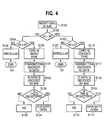
- CPU 11 performs data processing according to the processing program in the contact mode, which is stored in ROM 12.
- Each of the respective circuit blocks 12, 13, 14, 18, 19,... performs a processing operation in the contact mode.
- step S111 the encoder circuit 19 of the combination card 1 encodes ID data held in the EEPROM 14 of the combination card 1. Then, the combination card 1 transmits the encoded ID data to contact reader/writer 20 via contact I/F 15 and contact terminal 2.
- step S112 upon reception of the encoded ID data from the combination card 1, the contact reader/writer 20 decodes the encoded ID data.
- step S113 the contact reader/writer 20 judges whether or not the decoded ID data is already registered ID data .
- step S115 by ringing a buzzer while keeping the entrance gate locked, the contact reader/writer 20 informs that the decoded ID data is irregular ID data.
- step S113 If the decoded ID data is judged to be previously registered ID data in step S113(YES), the processing advances to step S114.
- step S114 the contact reader/writer 20 unlocks the gate of the main entrance 50.
- the CPU 11 performs data processing according to the processing program in the wireless mode, which is stored in the ROM 12.
- Each of the respective circuit blocks 12, 13, 14, 18, 19,... performs a processing operation in the wireless mode.
- step S131 the encoder circuit 19 of the combination card 1 encodes ID data held in the EEPROM 14 of the combination card 1. Then, the combination card 1 transmits the encoded ID data to the wireless reader/writer 21 via the wireless I/F 16 and the wireless antenna terminal 3.
- step S132 upon reception of the encoded ID data from the combination card 1, the wireless reader/writer 21 decodes the encoded ID data.
- step S133 the wireless reader/writer 21 judges whether or not the decoded ID data is already registered ID data.
- step S133 If the decoded ID data is judged not to be previously registered ID data in step S133(NO), the processing advances to step S135.
- step S135 by ringing a buzzer while keeping the gate of the sub entrance 51 locked, the wireless reader/writer 21 informs that the decoded ID data is irregular ID data.
- step S133 If the decoded ID data is judged to be previously registered ID data in step S133(YES), the processing advances to step S134.
- step S134 the wireless reader/writer 21 unlocks the gate of the sub entrance 51.
- the communication systems of the combination card can be separately used according to importance of security, importance of shortening of communication processing time, importance of easy communication actions, frequency of the communication actions and the like.
- the ID number is identification number represent, for example, one of account number, credit number, security number, PIN number and employee number.
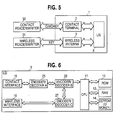
- Fig. 5 shows an arrangement of a combination card 1 according to a second embodiment of the present invention.
- a contact terminal 2 on the combination card 1, a contact terminal 2, a wireless antenna terminal 3 and a LSI chip 5 are mounted.
- contact terminal 2 is composed of respective external terminals (electrodes) such as a clock (CLOCK) terminal, a reset (RESET) terminal, a power source (VDD) terminal, a ground (GND) terminal and an input/output (I/O) terminal.
- Contact terminal 2 allows transmission/reception of various types of data by directly contacting those external terminals with a contact reader/writer 30.
- the wireless antenna terminal 3 is for executing transmission/reception of data with a wireless reader/writer 31, and for obtaining power from the wireless reader/writer 31.
- Fig. 6 shows an arrangement of the LSI chip 5 for a combination card according to the second embodiment of the present invention.
- the LSI chip 5 for a combination card according to the second embodiment of the present invention is different from the one shown in Fig. 2 in that the LSI chip 5 for a combination card includes encoder/decoder circuit 25, encoder/decoder circuit 26 and encoder/decoder circuit 27.
- the LSI chip 5 for a combination card does not include the switching circuit 17, the decoder circuit 18 and the encoder circuit 19.
- description will be made only for the differences between the LSI chip 5 for a combination card and the LSI chip 4 for a combination card according to the first embodiment of the present invention.
- the LSI chip 5 has: a contact-type interface 15 for outputting predetermined encoded data to the encoder/decoder circuit A25 when the predetermined encoded data is input to the combination card 1 via the contact terminal 2 similar to the first embodiment; and a wireless interface 16 for outputting encoded key data to encoder/decoder circuit 27 when encoded key data is input to the combination card 1 via the wireless antenna terminal 3.
- LSI chip 5 includes: the encoder/decoder circuit 25 connected to the contact interface 15, which is for decoding various data obtained by the contact reader/writer 30 and for encoding various data which is output by encoder/decoder circuit 26; encoder/decoder circuit 26 connected to encoder/decoder circuits 25 and 27, which is for encoding/decoding various data by use of key data obtained by the wireless reader/writer 31; and the encoder/decoder circuit C27 connected to the wireless I/F 16, which is for decoding/encoding the key data obtained by the wireless reader/writer 31.
- the encoder/decoder circuit A25 decodes the predetermined encoded data output from the contact I/F 15, and encodes predetermined data output from the encoder/decoder circuit B26.
- the encoder/decoder circuit B26 encodes predetermined data by use of the key data, and decodes the predetermined data encoded by use of the key data.
- the encoder/decoder circuit C27 decodes the encoded key data output from the wireless interface 16, and outputs the decoded key data to a second encoder/decoder circuit.
- step S201 a user first inserts the combination card 1 into the contact reader/writer 30.
- step S202 the combination card 1 receives key data for encoding/decoding from the wireless reader/writer 31 via the wireless antenna terminal 3 and the wireless I/F 16.
- step S203 an encoder/decoder circuit 27 of the combination card 1 decodes the received key data for encoding/decoding and outputs the decoded key data to an encoder/decoder circuit 26.
- step S204 by use of the key data output from the encoder/decoder circuit 27, the encoder/decoder circuit 26 of the combination card 1 encodes ID data held in an EEPROM 14 of the combination card 1, and then outputs the encoded ID data to an encoder/decoder circuit 25.
- step S205 the encoder/decoder circuit 25 of the combination card 1 further encodes the encoded ID data output from the encoder/decoder circuit 26.
- the encoder/decoder circuit 27 improves a security level by double encoding the ID data.
- step S206 the combination card 1 transmits the double-encoded ID data to the contact reader/writer 30 via the contact I/F 15 and contact terminal 2.
- step S207 upon reception of the encoded ID data from the combination card 1, the contact reader/writer 30 decodes the encoded ID data.
- step S208 the contact reader/writer 30 judges whether or not the decoded ID data is already registered ID data.
- step S208 If the decoded ID data is judged not to be the already registered ID data in the step S208, processing advances to step S209. In the step S209, the contact reader/writer 30 terminates communication processing.
- step S210 the contact reader/writer 30 notifies the user by displaying "Error” and the like.
- step S221 the contact reader/writer 30 encodes certification data and transmits the encoded certification data to the combination card 1 while the wireless reader/writer 31 encodes key data for encoding/decoding and transmits the encoded key data to the combination card 1.
- the certification data transmitted from the contact reader/writer 30 is input to the encoder/decoder circuit A via the contact terminal 2 of the combination card 1 and the contact I/F 15.
- the key data for encoding/decoding transmitted from the wireless reader/writer 31 is input to the encoder/decoder circuit C via the wireless antenna terminal 3 of the combination card 1 and the wireless I/F 16.
- the certification data transmitted herein is the one which has been already encoded by the contact reader/writer 30.
- the encoded certification data is the one obtained by further encoding the certification data previously encoded by the key data transmitted by the wireless reader/writer. In other words, the certification data has been double-encoded.
- the key data transmitted herein is the one previously encoded by the wireless reader/writer 31.
- step S222 the encoder/decoder circuit 27 of the combination card 1 decodes the key data for encoding/decoding received from the wireless reader/writer 31, and outputs the decoded key data to the encoder/decoder circuit 26.
- step S223 encoder/decoder circuit 25 of the combination card 1 decodes the certification data received from the contact reader/writer 30, and outputs the decoded certification data to the encoder/decoder circuit 26.
- step S224 by use of the key data output from encoder/decoder circuit 27, the encoder/decoder circuit 26 of the combination card 1 decodes the certification data output from the encoder/decoder circuit A25
- step S225 the combination card 1 starts to read money data held in the EEPROM 14 when confirmed that certification thereof is OK is received based on the decoded certification data.
- step S226 the combination card 1 receives the key data for encoding/decoding from the wireless reader/writer 31 via the wireless antenna terminal 3 and the wireless I/F 16.
- step S227 the encoder/decoder circuit 27 of combination card 1 decodes the received key data for encoding/decoding, and outputs the decoded key data to the encoder/decoder circuit 26.
- step S2208 by use of the key data output from the encoder/decoder circuit 27, encoder/decoder circuit 26 of combination card 1 encodes the money data held in the EEPROM 14 of the combination card 1. Then, the encoded money data is output to the encoder/decoder circuit 25.
- step S229 the encoder/decoder circuit 25 of the combination card 1 further encodes the encoded money data output from the encoder/decoder circuit B. Specifically, the encoder/decoder circuit 25 improves the security level of double encoding the money data.
- step S230 the combination card 1 transmits double-encoded money data to contact reader/writer 30 via the contact interface 15 and contact terminal 2.
- step S231 upon reception of the encoded money data from the combination card 1, the contact reader/writer 30 decodes the encoded money data.
- step S232 the contact reader/writer 30 displays the decoded money data and terminates the processing.
- certification is performed by the contact mode at the main entrance of the building, and by the wireless mode at the sub entrance in the building.
- the separate use of these wireless and contact modes is applicable other than the above.
- charging therefor may be performed by the contact mode.
- opening/closing of the gates may be performed by certifying the combination card by the wireless mode.
- opening/closing of a gate thereof may be performed by certifying the commutation ticket by the wireless mode.
- charging therefor may be performed by certification by the contact mode.
- the communication systems (the contact mode and the wireless mode) can be separately used according to a level of importance of a security (high or low) as described below.
- the combination card when used as a banking card, a convenience store card or the like, charging in a small-valve transaction may be performed by certifying the combination card by the wireless mode, and charging in a large-valve transaction may be performed by certifying the combination card by the contact mode.
- the ID number is identification number represent, for example, one of account number, credit number ,security number and PIN number.
- the transmitted/received data is encoded by performing the communications by use of both of the contact mode and the wireless mode, communications with the high security level can be performed.
- the present invention includes various embodiments and the like which are not described herein, as a matter of course. Therefore, a technological scope of the present invention is defined only by items specific to the invention according to claims pertinent based on the foregoing description.
Landscapes
- Engineering & Computer Science (AREA)
- Computer Hardware Design (AREA)
- Microelectronics & Electronic Packaging (AREA)
- Physics & Mathematics (AREA)
- General Physics & Mathematics (AREA)
- Theoretical Computer Science (AREA)
- Computer Networks & Wireless Communication (AREA)
- Credit Cards Or The Like (AREA)
- Mobile Radio Communication Systems (AREA)
Abstract
Description
Claims (17)
- A semiconductor integrated circuit comprising:a first interface circuit to output a low-level contact mode signal when no power supply voltage is supplied, -and to output a high-level contact mode signal when a power supply voltage is supplied;a second interface circuit to output a low-level wireless mode signal when no power supply voltage is supplied, and to output a high-level wireless mode signal when a power supply voltage is supplied;a switching circuit to switch a communication mode to a contact mode in the case of the high-level contact mode signal and the low-level raidio mode detecting signal, and to switch the communication mode to a wireless mode in the case of the low-level contact mode signal and the high-level wireless mode signal;a CPU to execute a processing program of the wireless mode in the wireless mode and to execute a processing program of the contact mode in the contact mode, according to the communication mode of the switching circuit;a memory circuit to store predetermined data; andan encoder circuit to encode the predetermined data held in the memory according to the wireless mode or the contact mode of the switching circuit.
- A semiconductor integrated circuit comprising, according to claim 1 wherein the first interface circuit is contact type circuit ,and receive/transmit data via contact reader/writer.
- A semiconductor integrated circuit comprising, according to claim 1 wherein the second interface circuit is wireless type circuit, and receive/transmit data via wireless communication.
- A semiconductor integrated circuit comprising, according to claim wherein the first interface circuit out put the low-level contact mode signal or high-level contact mode signal when the first interface circuit receive a signal from a contact type reader/writer.
- A semiconductor integrated circuit comprising, according to claim 1 wherein the second interface circuit output the low-level wireless mode signal or high-level wireless mode signal when the second interface circuit receive a signal from a non-contact type reader/writer.
- Semiconductor integrated circuit comprising:a first interface to output predetermined encoded data when the predetermined encoded data is input;a second interface to output encoded key data when the encoded key data is input;a first encoder/decoder circuit being coupled to the first interface that decode the predetermined encoded data output from the first interface;a second encoder/decoder circuit being coupled to the second interface that decode encoded key data output from the wireless interface and output decoded key data; anda third encoder/decoder circuit being coupled to the first encoder/decoder circuit, second encoder/decoder circuit and CPU that encode predetermined data by use of the decoded key data or that decode the predetermined data encoded by use of the decoded key data.
- The semiconductor circuit according to claim 6, wherein the first interface is contact type interface receiving data from a contact reader/writer.
- The semiconductor circuit according to claim 6, wherein the first interface is wireless type interface receiving data from a wireless reader/writer.
- A memory card comprising:a contact terminal to perform transmission/reception of first data, by electrically contacting with a contact reader/writer;a wireless antenna terminal to perform transmission/reception of second data by wirelessly communicating with a WIRELESS reader/writer;an semiconductor integrated circuit to generate a contact mode detecting signal when a power supply voltage is supplied from the contact terminal, to generating wireless mode detecting signal when a power supply voltage is supplied from the wireless antenna terminal, and to switch a communication mode according to the contact mode detecting signal and the wireless mode detecting signal.
- A memory card comprising:a contact terminal to perform transmission/reception of predetermined encoded data, by electrically contacting with a contact reader/writer;a wireless antenna terminal to perform transmission/reception of key data by wirelessly communicating with a wireless reader/writer;an integrated circuit to decode the predetermined encoded data input from the contact terminal, to decode encoded key data input from the wireless antenna terminal, and to encode predetermined data by use of the decoded key data or to decode the predetermined data encoded by the key data.
- A method of using a memory card comprising:outputting a contact mode detecting signal to a switching circuit when a power supply voltage is supplied to the memory card from a contact type reader/writer via a contact terminal;outputting a wireless mode detecting signal to the switching circuit when a power supply voltage is supplied to the memory card from a wireless type reader/writer via a wireless antenna terminal;encoding ID data held in a memory in the case of the contact mode detecting signal, and transmitting the encoded ID data to the contact type reader/writer via the contact terminal;decoding the received encoded ID data, judging whether or not the decoded ID data is registered ID data, and performing a predetermined operation by the contact type reader/writer when the decoded ID is the registered ID;encoding the ID data held in the memory in the case of a wireless mode detecting signal, and transmitting the encoded ID data to the wireless type reader/writer via the wireless antenna terminal; anddecoding the received encoded ID data, judging whether or not the decoded ID data is registered ID data and performing a predetermined operation by the wireless type reader/writer when the encoded ID is the registered ID.
- A method of using a memory card comprising:outputting a high-level contact mode detecting signal to a switching circuit when a power supply voltage is supplied to the memory card from a contact reader/writer via a contact terminal;outputting a low-level contact mode detecting signal to a switching circuit when a power supply voltage is not supplied to the memory card from a contact reader/writer via a contact terminal;outputting a high-level wireless mode detecting signal to the switching circuit when a power supply voltage is supplied to the memory card from a wireless type reader/writer via a wireless antenna terminal;outputting a low-level wireless mode detecting signal to the switching circuit when a power supply voltage is not supplied to the memory card from a wireless type reader/writer via a wireless antenna terminal;encoding ID data held in a memory in the case of the high-level contact mode detecting signal and a low-level wireless mode detecting signal, and transmitting the encoded ID data to the contact type reader/writer via the contact terminal;decoding the received encoded the ID data, judging whether or not the decoded ID data is the registered ID data and performing a predetermined operation by the contact type reader/writer; when the encoded ID data is the registered ID data;encoding the ID data held in the memory in the case of a low-level contact mode detecting signal and the high-level wireless mode detecting signal, and transmitting the encoded the ID data to the wireless type reader/writer via the wireless antenna terminal; anddecoding received the encoded ID data, judging whether or not the decoded ID data is the registered ID data and performing a predetermined operation by the wireless type reader/writer when the encoded ID data is registered ID data.
- The method of using a memory card according to claim 11 or 12, wherein the memory card is combination of contact type circuit and wireless type circuit.
- The method of using a memory card according to claim 11 or 12,where in the ID number is identification number represent one of account number, credit number and security number.
- A method of using a memory card comprising:decoding encoded key data received via a wireless type reader/writer;encoding ID data held in a memory by use of the decoded key data, and transmitting the encoded ID data to a contact type reader/writer;decoding the ID data by the contact type reader/writer;transmitting certification data, obtained by further encoding certification data encoded by key data, to the memory card by the contact type reader/writer in the case where the decoded ID data is registered ID data" and transmitting the encoded key data to the memory card by the wireless type reader/writer;decoding the encoded key data received from the wireless type reader/writer, and decoding the certification data obtained by further encoding the certification data encoded by the key data received from the contact type reader/writer;decoding the decoded certification data by use of the decoded key data;decoding the key data received from the wireless type reader/writer when certification of the combination card is confirmed based on the decoded certification data,;encoding predetermined data held in the memory by use of the decoded key data, further encoding the encoded predetermined data and transmitting the encoded predetermined data to the contact type reader/writer; anddecoding the encoded predetermined data received, and performing an predetermined operation by the contact reader/writer.
- The method of using a memory card according to claim 15, wherein the memory card is combination of contact type circuit and wireless type circuit.
- The method of using a memory card according to claim 15, the ID number is identification number represent one of an account number, credit number and security number.
Applications Claiming Priority (2)
| Application Number | Priority Date | Filing Date | Title |
|---|---|---|---|
| JP2001326761A JP2003132313A (en) | 2001-10-24 | 2001-10-24 | LSI for combination card, combination card and method of using combination card |
| JP2001326761 | 2001-10-24 |
Publications (2)
| Publication Number | Publication Date |
|---|---|
| EP1313063A2 true EP1313063A2 (en) | 2003-05-21 |
| EP1313063A3 EP1313063A3 (en) | 2003-08-20 |
Family
ID=19143093
Family Applications (1)
| Application Number | Title | Priority Date | Filing Date |
|---|---|---|---|
| EP02023675A Withdrawn EP1313063A3 (en) | 2001-10-24 | 2002-10-22 | Combination contact/contactless IC card |
Country Status (3)
| Country | Link |
|---|---|
| US (1) | US20030075601A1 (en) |
| EP (1) | EP1313063A3 (en) |
| JP (1) | JP2003132313A (en) |
Cited By (5)
| Publication number | Priority date | Publication date | Assignee | Title |
|---|---|---|---|---|
| WO2005069207A1 (en) * | 2003-12-17 | 2005-07-28 | Gemplus | Immunity to variations in limited resources supplied to an object having a dual interface |
| US7365642B2 (en) | 2004-02-24 | 2008-04-29 | Sony Corporation | Semiconductor integrated circuit, mobile module, and message communication method |
| EP1998276A3 (en) * | 2007-05-28 | 2009-09-23 | Incard SA | IC Card comprising a main device and an additonal device |
| FR2937212A1 (en) * | 2008-10-15 | 2010-04-16 | Sagem Defense Securite | SECURE COMMUNICATION DEVICE. |
| CN105938570A (en) * | 2016-05-11 | 2016-09-14 | 新智数字科技有限公司 | Smart card |
Families Citing this family (15)
| Publication number | Priority date | Publication date | Assignee | Title |
|---|---|---|---|---|
| US7472834B2 (en) * | 2003-07-09 | 2009-01-06 | Stmicroelectronics S.A. | Dual-mode smart card |
| US7237719B2 (en) * | 2003-09-03 | 2007-07-03 | Stmicroelectronics, Inc. | Method and apparatus for a USB and contactless smart card device |
| JP4666943B2 (en) * | 2004-04-23 | 2011-04-06 | 株式会社エヌ・ティ・ティ・ドコモ | ID tag, tag reader, ID tag security system, and ID tag transmission restoration method |
| JP4981271B2 (en) * | 2004-07-05 | 2012-07-18 | 三星電子株式会社 | Multi-mode integrated circuit device including mode detection and operation method thereof |
| KR101038109B1 (en) * | 2004-07-05 | 2011-06-01 | 삼성전자주식회사 | Smart Card System with Dual Interface Mode |
| JP4643342B2 (en) * | 2005-04-11 | 2011-03-02 | 株式会社エヌ・ティ・ティ・ドコモ | Information management apparatus and information management method |
| FR2888976B1 (en) * | 2005-07-25 | 2007-10-12 | Oberthur Card Syst Sa | ELECTRONIC ENTITY WITH CONTACT AND REMOTE COMMUNICATION MEANS |
| JP2007257542A (en) * | 2006-03-24 | 2007-10-04 | Toshiba Corp | Composite portable electronic device and composite IC card |
| JP2007257543A (en) * | 2006-03-24 | 2007-10-04 | Toshiba Corp | Composite portable electronic device and composite IC card |
| JP4960034B2 (en) * | 2006-07-27 | 2012-06-27 | 株式会社東芝 | Information storage medium and information storage medium processing apparatus |
| JP4519935B2 (en) | 2008-12-26 | 2010-08-04 | 株式会社東芝 | Information communication method, communication terminal device, and information communication system |
| KR101939237B1 (en) * | 2011-06-14 | 2019-01-17 | 삼성전자 주식회사 | Internal voltage generating circuit and smart card |
| US20140372653A1 (en) * | 2013-06-13 | 2014-12-18 | Transcend Information, Inc. | Storage Device with Multiple Interfaces and Multiple Levels of Data Protection and Related Method Thereof |
| JP2015114998A (en) * | 2013-12-13 | 2015-06-22 | 凸版印刷株式会社 | Portable information processing apparatus, information processing method, and program |
| WO2018063438A1 (en) * | 2016-09-29 | 2018-04-05 | The Regents Of The University Of California | Visible light communication system-on-a-chip |
Family Cites Families (18)
| Publication number | Priority date | Publication date | Assignee | Title |
|---|---|---|---|---|
| US5293029A (en) * | 1989-01-17 | 1994-03-08 | Kabushiki Kaisha Toshiba | System for mutually certifying an IC card and an IC card terminal |
| DE3935364C1 (en) * | 1989-10-24 | 1990-08-23 | Angewandte Digital Elektronik Gmbh, 2051 Brunstorf, De | |
| JPH04143881A (en) * | 1990-10-05 | 1992-05-18 | Toshiba Corp | Mutual authentication method |
| US5396558A (en) * | 1992-09-18 | 1995-03-07 | Nippon Telegraph And Telephone Corporation | Method and apparatus for settlement of accounts by IC cards |
| JPH10505932A (en) * | 1995-06-02 | 1998-06-09 | フィリップス エレクトロニクス ネムローゼ フェンノートシャップ | Chip card |
| DE19531372A1 (en) * | 1995-08-25 | 1997-02-27 | Siemens Ag | Smart card |
| DE19604045A1 (en) * | 1996-02-05 | 1997-08-07 | Siemens Ag | Device for processing and storing data |
| JP3360002B2 (en) * | 1996-03-14 | 2002-12-24 | 沖電気工業株式会社 | Contact / non-contact IC card and contact / non-contact IC card reader / writer |
| FR2752076B1 (en) * | 1996-08-05 | 1998-09-11 | Inside Technologies | ELECTRICAL SUPPLY SYSTEM FOR MICROCIRCUIT WITH MIXED OPERATION, WITH OR WITHOUT CONTACT |
| IL119943A (en) * | 1996-12-31 | 2000-11-21 | On Track Innovations Ltd | Contact/contactless data transaction card |
| KR100565879B1 (en) * | 1997-09-23 | 2006-03-31 | 코닌클리케 필립스 일렉트로닉스 엔.브이. | Dual-mode data carriers with potential equalization means for equalizing the potentials of at least two contact terminals and circuitry for such data carriers |
| CN1135497C (en) * | 1997-09-23 | 2004-01-21 | 皇家菲利浦电子有限公司 | Dual-mode data carrier and circuit for such a data carrier with improved mode change-over |
| IL122841A0 (en) * | 1997-12-31 | 1998-08-16 | On Track Innovations Ltd | Smart card for effecting data transfer using multiple protocols |
| ATE430340T1 (en) * | 1998-03-24 | 2009-05-15 | Toshiba Kk | PORTABLE ELECTRONIC DEVICE HAVING CONTACT AND CONTACTLESS INTERFACES |
| DE19816417A1 (en) * | 1998-04-14 | 1999-10-28 | Angewandte Digital Elektronik | Chip card with electronic blocking function |
| JPH11338982A (en) * | 1998-05-25 | 1999-12-10 | Mitsubishi Electric Corp | IC memory card system device and IC memory card thereof |
| EP1117064B1 (en) * | 1998-07-31 | 2005-01-26 | Matsushita Electric Industrial Co., Ltd. | A dual-purpose non-contact chip card, a system with terminal appartus and card, and a communication method |
| JP3657178B2 (en) * | 2000-07-10 | 2005-06-08 | 沖電気工業株式会社 | IC card |
-
2001
- 2001-10-24 JP JP2001326761A patent/JP2003132313A/en not_active Abandoned
-
2002
- 2002-10-22 EP EP02023675A patent/EP1313063A3/en not_active Withdrawn
- 2002-10-23 US US10/277,873 patent/US20030075601A1/en not_active Abandoned
Cited By (9)
| Publication number | Priority date | Publication date | Assignee | Title |
|---|---|---|---|---|
| WO2005069207A1 (en) * | 2003-12-17 | 2005-07-28 | Gemplus | Immunity to variations in limited resources supplied to an object having a dual interface |
| US7365642B2 (en) | 2004-02-24 | 2008-04-29 | Sony Corporation | Semiconductor integrated circuit, mobile module, and message communication method |
| EP1998276A3 (en) * | 2007-05-28 | 2009-09-23 | Incard SA | IC Card comprising a main device and an additonal device |
| US8042743B2 (en) | 2007-05-28 | 2011-10-25 | Incard Sa | IC card comprising a main device and an additional device |
| FR2937212A1 (en) * | 2008-10-15 | 2010-04-16 | Sagem Defense Securite | SECURE COMMUNICATION DEVICE. |
| WO2010043679A1 (en) * | 2008-10-15 | 2010-04-22 | Sagem Defense Securite | Secure communication device |
| GB2476023A (en) * | 2008-10-15 | 2011-06-08 | Sagem Dofonse Socurito | Secure communication device |
| GB2476023B (en) * | 2008-10-15 | 2013-05-15 | Sagem Defense Securite | Secure communication device |
| CN105938570A (en) * | 2016-05-11 | 2016-09-14 | 新智数字科技有限公司 | Smart card |
Also Published As
| Publication number | Publication date |
|---|---|
| EP1313063A3 (en) | 2003-08-20 |
| JP2003132313A (en) | 2003-05-09 |
| US20030075601A1 (en) | 2003-04-24 |
Similar Documents
| Publication | Publication Date | Title |
|---|---|---|
| US20030075601A1 (en) | Semiconductor integrated circuit, memory card having the semiconductor integrated circuit and method of using the memory card | |
| US5613159A (en) | Contact-free data exchange between a terminal and modular portable set having two different protocols for exchange which is selected based on portable set type | |
| CN101820696B (en) | Terminal supporting enhanced near field communication and processing method thereof | |
| US8566588B2 (en) | Method of authentication and secure exchange of data between a personalised chip and a dedicated server, and assembly for implementing the same | |
| US10474802B2 (en) | Biometric enrolment authorisation | |
| KR101582682B1 (en) | Smart card telephone comprising such a card and method for executing a command in such a card | |
| JP4412162B2 (en) | User authentication device and entrance / exit management device | |
| US7815125B2 (en) | Microprocessor card | |
| CA2237657C (en) | Power transmission system, power transmission/communication system and reader and/or writer | |
| EP4113361A1 (en) | Method for managing a contactless card | |
| US7121472B2 (en) | Semiconductor integrated circuit, semiconductor integrated circuit module and information apparatus | |
| US20060086806A1 (en) | Dual-mode smart card | |
| US10609012B2 (en) | Method of operating a security token, computer program product and security token | |
| CN100483456C (en) | Inductively coupled exchange in a portable smart object with central and peripheral circuitry | |
| KR20100125776A (en) | Chip card with contact and contactless mode and method of operation thereof | |
| JP3589029B2 (en) | Reader / writer, non-contact IC card and card system using them | |
| US6637664B1 (en) | Composite IC card | |
| KR101928078B1 (en) | Authentication medium case and method for managing entrance-exit using the same | |
| JP2021009593A (en) | Non-contact ic card with fingerprint authentication function, and fingerprint authentication system using thereof | |
| JP3838901B2 (en) | Contact / contactless IC card | |
| KR100411584B1 (en) | A CARD READER SUPPORTING CONTACT-TYPE SMART CARD and CONTACTLESS-TYPE SMART CARD AND A CARD READER CONTROLLING METHOD | |
| KR100480516B1 (en) | Smart card module mounted in the wire/wireless communication terminal | |
| CN113013995B (en) | Power supply management method | |
| US9087230B2 (en) | Method for communicating by a detector of the presence of chip cards in a reader chip cards and a reading device communicating by the presence detector | |
| JPH02226392A (en) | Card identification device |
Legal Events
| Date | Code | Title | Description |
|---|---|---|---|
| PUAI | Public reference made under article 153(3) epc to a published international application that has entered the european phase |
Free format text: ORIGINAL CODE: 0009012 |
|
| 17P | Request for examination filed |
Effective date: 20021022 |
|
| AK | Designated contracting states |
Designated state(s): AT BE BG CH CY CZ DE DK EE ES FI FR GB GR IE IT LI LU MC NL PT SE SK TR |
|
| AX | Request for extension of the european patent |
Extension state: AL LT LV MK RO SI |
|
| PUAL | Search report despatched |
Free format text: ORIGINAL CODE: 0009013 |
|
| AK | Designated contracting states |
Designated state(s): AT BE BG CH CY CZ DE DK EE ES FI FR GB GR IE IT LI LU MC NL PT SE SK TR |
|
| AX | Request for extension of the european patent |
Extension state: AL LT LV MK RO SI |
|
| 17Q | First examination report despatched |
Effective date: 20031030 |
|
| AKX | Designation fees paid |
Designated state(s): DE FR GB |
|
| STAA | Information on the status of an ep patent application or granted ep patent |
Free format text: STATUS: THE APPLICATION IS DEEMED TO BE WITHDRAWN |
|
| 18D | Application deemed to be withdrawn |
Effective date: 20040511 |