EP1312947A2 - Photonic crystal and optical waveguide elements - Google Patents
Photonic crystal and optical waveguide elements Download PDFInfo
- Publication number
- EP1312947A2 EP1312947A2 EP02255907A EP02255907A EP1312947A2 EP 1312947 A2 EP1312947 A2 EP 1312947A2 EP 02255907 A EP02255907 A EP 02255907A EP 02255907 A EP02255907 A EP 02255907A EP 1312947 A2 EP1312947 A2 EP 1312947A2
- Authority
- EP
- European Patent Office
- Prior art keywords
- photonic crystal
- refractive index
- periodicity
- optical waveguide
- photonic
- Prior art date
- Legal status (The legal status is an assumption and is not a legal conclusion. Google has not performed a legal analysis and makes no representation as to the accuracy of the status listed.)
- Withdrawn
Links
Images







Classifications
-
- G—PHYSICS
- G02—OPTICS
- G02B—OPTICAL ELEMENTS, SYSTEMS OR APPARATUS
- G02B6/00—Light guides; Structural details of arrangements comprising light guides and other optical elements, e.g. couplings
- G02B6/10—Light guides; Structural details of arrangements comprising light guides and other optical elements, e.g. couplings of the optical waveguide type
- G02B6/12—Light guides; Structural details of arrangements comprising light guides and other optical elements, e.g. couplings of the optical waveguide type of the integrated circuit kind
- G02B6/122—Basic optical elements, e.g. light-guiding paths
- G02B6/1225—Basic optical elements, e.g. light-guiding paths comprising photonic band-gap structures or photonic lattices
-
- B—PERFORMING OPERATIONS; TRANSPORTING
- B82—NANOTECHNOLOGY
- B82Y—SPECIFIC USES OR APPLICATIONS OF NANOSTRUCTURES; MEASUREMENT OR ANALYSIS OF NANOSTRUCTURES; MANUFACTURE OR TREATMENT OF NANOSTRUCTURES
- B82Y20/00—Nanooptics, e.g. quantum optics or photonic crystals
Definitions
- the present invention relates to the technical areas of photonic crystals and optical waveguide elements employing the same, and more specifically, to the technical areas of photonic crystals capable of forming full photonic band gaps and optical waveguide elements employing the same.
- they can be produced by periodically arranging areas of differing refractive indexes into a structure comprised of materials having specific refractive indexes.
- Conventional photonic crystals mimicking crystals present in the natural world, for example, exploit the periodicity based on translational symmetry that is observed in trigonal, tetragonal, and similar lattices.
- the photonic crystals When employing photonic crystals in various precision optical equipment and the like, the photonic crystals are required to completely block light of specific wavelengths.
- conventional photonic crystals having periodic structures of translational symmetry have problems in that they are dependent on the direction of propagation of light, and the wavelengths of the photonic band gaps formed vary (referred to below as "directional dependence on photonic band gap").
- directional dependence on photonic band gap a broad range of photonic band gaps are formed to impart overlapping gaps and ensure blocking of light propagating in all directions. Imparting a broad range of photonic band gaps requires employing a structure of materials in which the photonic crystals have large differences in refractive index. In the natural world, air has the lowest refractive index.
- optical waveguide elements employing photonic crystals have been the focus of great attention. These are devices in which linear defects of noncrystalline structure are formed in photonic crystals, light is confined to the defects, and the light propagates along the defects. Since the optical waveguide paths of photonic crystals have the property of strongly confining light by means of the existence of photonic band gaps, they afford the advantage of less light loss than conventional optical waveguide paths. Their application to various optical circuits is anticipated. However, two-dimensional photonic crystals having conventional trigonal and tetragonal lattices are problematic in that the introduction of defects is limited.
- the present invention devised in light of the various above-described problems, has for its object to provide a novel photonic crystal capable of blocking light in all propagation directions and permitting the formation of a full photonic band gap.
- the present invention also has the object of providing a novel photonic crystal without directional dependence of the photonic band gap.
- the present invention has the still further object of providing a novel photonic crystal reducing restrictions on the selection of constituent materials and on manufacturing.
- the present invention has the additional object of providing optical waveguide elements affording low optical loss and a reduction in the restrictions on shape in the formation of optical waveguides.
- the present invention has the still further object of providing an optical waveguide capable of reducing restrictions on the design of optical circuits when applied to optical circuits.
- a photonic crystal having a structure of which the refractive index changes with a periodicity defined in a polar coordinate system.
- the photonic crystal in which refractive index changes between two values of n 1 and n 2 (where n 1 is not equal to n 2 ) based on a periodicity defined in a polar coordinate system; the photonic crystal wherein said periodicity is of a non-translational symmetry; the photonic crystal wherein said periodicity has a rotational symmetry; the photonic crystal wherein the refractive index changes based on a periodicity that is two-dimensionally defined in a polar coordinate system; and the photonic crystal in which a structural unit comprising a first material having a refractive index of n 1 and a second material having a refractive index of n 2 (where n 1 is not equal to n 2 ) repeatedly occurs at positions rotated by a ⁇ degree (0 ⁇ ⁇ ⁇ 360) about a point serving as the center of a polar coordinate system; the photonic crystal in which a region having a refractive index differing from air in space is arranged with a periodicity defined by
- a photonic crystal comprising plural elements with a refractive index n 1 , arranged in a two-dimensional rotational symmetry lattice; and plural spaces with a refractive index n 2 (where n 1 is not equal to n 2 ) between adjacent said elements.
- an optical waveguide element comprising a photonic crystal having a structure of which the refractive index changes with a periodicity defined in a polar coordinate system, optical inlet and outlet regions on the surface of said photonic crystal, and a defect region of incomplete photonic crystal periodicity formed within said photonic crystal, wherein said defect region functions as an optical waveguide path by guiding from said inlet region to said outlet region an optical signal incapable of propagating through the photonic band gap of said photonic crystal.
- the optical waveguide element wherein said photonic crystal has the structure in which refractive index changes between two values of n 1 and n 2 (where n 1 is not equal to n 2 ) based on a periodicity defined in a polar coordinate system; the optical waveguide element wherein said photonic crystal periodicity is of a non-translational symmetry; the optical waveguide element wherein said photonic crystal periodicity has a rotational symmetry; the optical waveguide element wherein said photonic crystal periodicity is two-dimensionally defined in a polar coordinate system; the optical waveguide element wherein said photonic crystal is in which a structural unit comprising a first material with a refractive index of n 1 and a second material with a refractive index of n 2 (where n 1 is not equal to n 2 ) repeatedly occurs at positions rotated by a ⁇ degree (0 ⁇ 360) about a point serving as the center of a polar coordinate system; the optical waveguide element wherein said photonic crystal is in which a region having
- an optical waveguide element comprising:
- the photonic crystal of the present invention is characterized by having changes in refractive index within the structure based on periodicity defined in a polar coordinate system.
- This periodicity defined in a polar coordinate system may be either two-dimensional or three-dimensional.
- the term "photonic crystal” does not mean a conventional photonic crystal having within its structure a change in refractive index having translational symmetry, but rather is used in a manner including all structures having internal changes in refractive index capable of forming a photonic band gap. So long as the requirements of the present invention are satisfied, photonic crystals not included in the conventional definition of "photonic crystals" fall within the scope of the present invention.
- peripherality defined in a polar coordinate system means a state in which an identical base structure is arranged in repeating fashion in polar coordinate space. Taking the example of a two-dimensional polar coordinate system, this refers to a state having a structure repeatedly exhibiting the same arrangement at a position rotated by a certain angle about a center point.
- periodicities examples are a periodicity having a two-rotation symmetry in which the same structural unit repeatedly appears with each rotation of 180°; a periodicity having a three-rotation symmetry in which the same structural unit repeatedly appears with each rotation of 120°; and a periodicity having a four-rotation symmetry in which the same structural unit repeatedly appears with each rotation of 90°.
- a periodicity having a single symmetry in which the same structural unit does not repeat unless rotated 360° is also included herein.
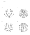
- Figs. 1(a) through (d) show a three-rotation symmetry, four-rotation symmetry, five-rotation symmetry, and six-rotation symmetry, respectively.
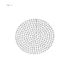
- Fig. 2 shows a single-rotation symmetry arrangement. The present invention can be applied to all of these.
- periodicity defined by a polar coordinate system there are numerous rotational symmetries.
- a periodicity having rotational symmetry is desirably employed in the present invention.
- periodicities defined in polar coordinate systems may have arrangements that may be periodic in rectangular coordinate systems, that is, may have translational symmetry, so long as there is a structure the refractive index of which changes based on a periodicity defined in a polar coordinate system, irrespective of whether or not a translational symmetry exists, the structure is covered by the present invention.
- a periodicity without translational symmetry is desirable.
- the photonic crystal of the present invention is characterized by having a structure in which the refractive index changes based on a periodicity defined by a polar coordinate system. Normally, in a photonic crystal, there are two values defining the change in refractive index, and the greater the difference in the two values of refractive index, the greater the photonic band gap.
- the refractive index is specific to the material. Examples of materials having high refractive indexes of greater than or equal to 2 are: diamond (2.41), Si (about 3), TiO 2 (2.6), and Ta 2 O 5 (2.3). Examples of materials having low refractive indexes are SiO 2 and optical glass.
- the photonic crystal of the present invention is configured of Ta 2 O 5 or the like as a high refractive index range, and something other than air as the low refractive index range, such as a low refractive index material such as SiO 2 , permitting the formation of a full photonic band gap. Nor does the photonic crystal of the present invention preclude the formation of air regions.
- the period of the refractive index is not specifically limited, and may be determined based on the wavelength of the light that is to be blocked. For example, when the objective is to block visible light or near infrared radiation, it suffices to change the period of the refractive index by about the same amount as the wavelength of visible light or near infrared radiation.
- photonic crystal of the present invention it suffices to incorporate into some portion thereof a structure in which the refractive index changes based on a periodicity defined by polar coordinates.
- photonic crystals configured by arranging structures in which the refractive index changes based on a periodicity defined by polar coordinates into a two-dimensional arrangement having translational symmetry are also covered by the photonic crystal of the present invention.
- photonic crystals having a structure in which the refractive index changes based on a two-dimensional periodicity defined by polar coordinates are covered by the present invention; that is, photonic crystals having a structure having a refractive index that does not change based on a periodicity that is three-dimensionally defined by polar coordinates are also covered by the present invention.
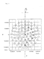
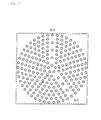
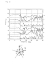
- the arrangement of two-dimensional periodicity can be accomplished, for example, as the arrangement of rotational symmetry shown in Fig. 3.
- an "O” denotes the position of a rod, and the number within the "O” is used to denote the position.
- the same array repeatedly appears at positions rotated by 72° about the center (position 76) of the polar coordinates, that is, is an arrangement having a five-rotation symmetry.
- the rod arrangement does not have periodicity in rectangular coordinates; it is an arrangement without translational symmetry.
- a structure obtained by arranging rods consisting of a material with a refractive index of 1.92 at the positions indicated by the 76 circles shown in Fig. 3 with each pair of rods having a center distance D (denoted by D in Fig. 3) between them of 85 micrometers was employed as the computational model.
- the diameter R 0 of the bottom surface of the rods (denoted by R 0 in Fig. 3) was made 22 micrometers, and the height of the rods was made infinitely large.
- the photonic band gap present can be demonstrated by irradiating light from within a photonic crystal and showing that light of specific wavelength does not leak to the outside, due to the properties of light, the same demonstration can be effected by reversing the arrival position and irradiation position of the light.
- Fig. 4 gives the computation results.
- Fig. 4 shows graphs in which the frequency of light is plotted on the x-axis and the intensity of the light on the y-axis for light arriving at positions a-e.
- the computational results of Fig. 4 show that the light reaching any of the positions had an intensity at a frequency of about 50 cm -1 that was extremely low. That is, in the model of the photonic crystal having a periodicity defined in the polar coordinate system shown in Fig. 3, the computations demonstrate that a photonic band gap was formed for light having a frequency of about 50 cm -1 . In these calculations, TM mode polarization was employed. However, such a photonic band gap can also be formed for TE mode polarization.
- Fig. 5(a) shows the absolute value of the pointing vector of light reaching position c for TE mode polarization
- Fig. 5(b) shows the same for TM mode polarization.
- the x axis denotes the frequency cm -1 (1 to 200, 400 points), and the y axis denotes the displacement (angle of incidence) in the direction of incidence of the light.
- the intensity of the absolute value of the pointing vector of the light is denoted by color darkness in the figures (by color in original figures). As will be understood from the scale recorded beneath the graphs, the pointing vector was most weak in the portions of dark color (dark blue in original figures). In both Figs. 5(a) and (b), there were regions of low pointing vectors near a frequency of 50 cm -1 that are denoted as areas of dark color bands in the contour line drawings. These results indicate that in this photonic crystal model, the wavelength of the photonic band gap did not vary even when the direction of incident light was varied.
- Fig. 6 consists of contour graphs of the absolute values of the pointing vectors of light reaching the positions of rods 4, 5, 9, 10, 14, and 15 (calculated for TM mode polarization). The number recorded at the upper left of each of the contour line graphs indicates the position of the rod. In the contour line graphs of all of the positions of Fig.
- the computations were performed for electromagnetic waves on the order of millimeter-waves, but similar results would be obtained for computations on visible light to near infrared radiation. That is, with the photonic crystal of the embodiment, it is possible to form photonic crystals for visible light to near infrared radiation. In this embodiment, it suffices to position the rods to achieve a period with a wavelength of from visible light to near infrared.
- a photonic crystal having a configuration in which rods of a material other than air were arranged in air.
- Semiconductors such as Si and GaAs are materials of comparative high refractive index for which micromachining technology is highly developed. These materials are thus desirable for use as the above-mentioned structures. For example, Sugimoto, Y. et al., Journal of Applied Physics, Vol. 91, p. 922 (2002), Fig.
- the photonic crystal of the present invention can be fabricated by machining holes at the positions denoted by "O" in the figures based on the polar coordinates given in Figs. 1 through 3 on the x-y plane of a structure comprised of a semiconductor using the techniques employed in the cited literature.
- the use of micromachining techniques permits the fabrication of photonic crystals in which a photonic gap band is present for light in the visible and infrared regions.
- a photonic crystal of a structure in which a structural unit comprised of a material (other than air) having a refractive index n 1 (other than air) and a material having a refractive index n 2 (where n 1 is not equal to n 2 ) is arranged with a periodicity defined by polar coordinates, specifically, in which the constitutional unit of the second material (other than air) has a structure repeating at a rotational position of precisely a certain angle about a center in the form of some point in the coordinate axis system.
- the present embodiment affords the advantage of high strength, since no space is formed in the structure.
- the incorporation of a structure having a refractive index changing with a periodicity defined by polar coordinates reduces the wavelength shift of the photonic band gap. Accordingly, due to the large difference in refractive index within the structure, there is no need to form voids, and, for example, even in a configuration comprising a combination of materials of comparatively low difference in refractive index, such as SiO 2 and Ta 2 O 5 , it is possible to block light in all directions of propagation.
- the photonic crystal of the present implementation mode may be produced, for example, by a manufacturing method comprising a step of forming on a substrate surface irregularities arranged with a two-dimensional periodicity defined by a polar coordinate system, and a step of stacking a layer comprised of a material having a refractive index of n 1 and a layer having a refractive index of n 2 on the substrate surface having irregularities.
- a manufacturing method comprising a step of forming on a substrate surface irregularities arranged with a two-dimensional periodicity defined by a polar coordinate system, and a step of stacking a layer comprised of a material having a refractive index of n 1 and a layer having a refractive index of n 2 on the substrate surface having irregularities.
- a structure in which the refractive index changes with three-dimensional periodicity can be manufactured by, for example, stacking multiple films (for example, films comprised of a material having a refractive index of n 1 and a refractive index of n 2 ) on a substrate having surface irregularities by bias sputtering or the like.
- the photonic crystal of the present invention can be used to control electromagnetic waves, and is desirably employed as an optical waveguide element to control the direction of propagation of light. Further, an optical waveguide element employing the photonic crystal of the present invention can be employed in three-dimensional optical circuits, optical devices, and light-emitting devices. Since the photonic crystal of the present invention forms a full photonic band gap, when employed in light-emitting devices, for example, it can be expected to substantially improve light-emission efficiency.
- This embodiment of the present invention is an optical waveguide element comprised of the photonic crystal of the present invention, inlet and outlet regions formed in the surface of the photonic crystal, and a defect region formed in the photonic crystal and imparting incomplete periodicity to the photonic crystal.
- the defect region functions as an optical waveguide path guiding from the inlet region to the outlet region light that is incapable of propagating due to the photonic band gap of the photonic crystal.
- the presence of the photonic band gap of the photonic crystal confines entering light to the defect region formed in the photonic crystal and acts as an optical waveguide permitting the propagation of the confined light along the defect region.
- the use of the presence of the photonic band gap of the photonic crystal to confine light results in little loss of light by reflection or the like.
- the use of a photonic crystal in which the index of refraction changes by having a periodicity defined by a polar coordinate system the restrictions on the shape of the defect region that can be internally formed are reduced, and defect regions of various shapes can be formed. Accordingly, it is possible to readily form defect regions causing light to propagate in a desired direction, and when applied to optical circuits, permits a widening of the degree of freedom in the designing of optical circuits.
- This embodiment of the optical waveguide element of the present invention is an optical waveguide element employing a photonic crystal having a two-dimensional periodicity of rotational symmetry in which a structural unit comprised of a first material of refractive index n 1 and a second material of refractive index n 2 (where n 1 does not equal n 2 ) occurs repeatedly at positions of prescribed rotation about some point as center of a polar coordinate system.
- An optical waveguide element employing a photonic crystal having a periodicity with rotational symmetry in the x-y plane (letting the z direction be infinitely large) shown in Fig. 7 will be described as an embodiment of the present invention.
- An optical waveguide element can be obtained by forming a defect region of incomplete periodicity in the photonic crystal exhibiting rotational symmetry shown in Fig. 7.
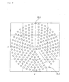
- One example of optical waveguide element of the present invention can be fabricated by taking two points on the circumference as the light inlet and outlet regions and removing the rods from a region connected through the center of the circle passing through these two points to form a defect region (for example, the space in which no "O"s are arranged in Fig. 8, with the z direction being infinite space), which functions as an optical waveguide path.
- Another example can be fabricated by taking two points on the circumference as the light inlet and outlet regions and removing the some rods from a region connected through the center of the circle passing through these two points to form a defect region (for example, the space in which no "O"s are arranged at interval of one "O" in Fig. 12, with the z direction being infinite space), which functions as an optical coupled cavity waveguide path.
- a defect region for example, the space in which no "O"s are arranged at interval of one "O" in Fig. 12, with the z direction being infinite space
- a linear defect intersecting at 60 degrees, 120 degrees, or 90 degrees due to the periodicity of the photonic crystal it is only possible to incorporate a linear defect intersecting at 60 degrees, 120 degrees, or 90 degrees due to the periodicity of the photonic crystal.
- the range of selection of the angle of bend of the defect region is broadened.
- photonic crystals exhibiting two-dimensional rotational symmetry it is possible to take two points on the circumference as the optical inlet and outlet, form a defect region linking these two points through the center of the circle, and bend the direction of light propagation by any angle based on the number n of rotational symmetry.
- Figs. 8 through 10 show embodiments in which points on the circumference of the photonic crystal shown in Fig. 7 are taken as the optical inlet and outlet and defect regions are formed along axes of rotational symmetry.
- the optical waveguide element shown in Fig. 8 is an embodiment in which the points of intersection of two of the five-rotation symmetry axes with the circumference are taken as an optical inlet SL0 and outlet SL2, and a defect region is formed linking point SL0 and point SL2 through the center SL1 of the circle. Light enters through point SL0, is confined to the defect region, propagates along the defect region, and arrives at point SL2.
- the optical waveguide element of the periodic structure shown in Fig. 8 permits the bending of the direction of propagation by about 144 degrees while controlling the loss of light. Further, by varying the combination of the five-rotation symmetry axes forming the defect region, it is possible to configure an optical waveguide element bending by about 72 degrees in the direction of propagation of the light.
- the optical waveguide element shown in Fig. 9 is an embodiment in which the two points SL2 and SL4 on the circumference are taken as outlets, point SL0 is taken as inlet, and a defect region is formed linking these points through the center SL1 of the circle.
- this optical waveguide element there is a fork in the direction of light propagation.
- the optical waveguide element of Fig. 10 is an embodiment in which rods positioned along all five of the five-rotation axes are removed to form defect regions.
- this optical waveguide element when light entering at point SL0 propagates along the defect regions and reaches the center SL1 of the circle, it branches in four directions along the defect regions, reaching SL2 through SL5.
- a photonic crystal in the shape of a fan defined by two radii comprised of straight lines and a segment of the circumference in the form of a curved line can be used to form an optical waveguide element.
- this photonic crystal can also be used as an optical waveguide element in which the direction of advance of the light is an arc-shaped bend.
- light inlet SL0 and outlet SL2 can be formed in radii and a defect connecting SL0 and SL2 in an arc can be formed to configure an optical waveguide element in which the direction of advancement of light is bent in an arc.
- optical defect waveguide elements there are shown embodiments of optical defect waveguide elements in Figs. 8 through 11, however, the photonic crystal of the present invention may also be employed coupled cavity waveguide.
- the optical waveguide element shown in Fig. 12 is a coupled cavity waveguide element which may be fabricated by removing rods at interval of a rod, not removing as all rods as Fig. 8, from a region connected through the center passing through SL0 to SL2 to form a defect region in the photonic crystal as shown in Fig. 7.
- the defect region shown in Fig. 8 was formed in the photonic crystal shown in Fig. 7 and the following calculations were made of the transmitted spectrum at position SL2 in the figure to confirm operation as an optical waveguide element.
- Fig. 13 consists of graphs showing the results with light frequency plotted on the x-axis and light intensity on the y-axis.
- the computational results of Fig. 13 reveal that a photonic band gap was present in the structure of Fig. 7 with its center at 50 cm -1 .
- the transmitted spectrum at SL2 was computed from a computational model obtained by removing multiple rods from the structure shown in Fig. 7 to form an internal defect region and achieve the structure shown in Fig. 8. Specifically, the rods positioned on two of the five-rotation symmetry axes, or a total of 19 rods, were removed from positions of five-rotation symmetry in Fig. 7 to form defect regions. It was assumed that light corresponding to millimeter-waves (frequency of from 0 to 200 cm -1 ) was irradiated at SL0, and the transmitted spectrum reaching position SL2 was computed.
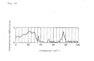
- Fig. 14 gives the computational results.
- Fig. 14 is a graph showing the computation results with light frequency plotted on the x-axis and transmission efficiency plotted on the y-axis.
- a transmission efficiency peak is present near 52 cm -1 , the point where the light intensity was 0 in Fig. 13.
- the results reveal that a transmission mode was present in the structure of Fig. 8.
- a photonic band gap was present in the structure of Fig. 7, with 40 to 80 cm -1 electromagnetic waves being unable to pass through the structure.
- propagation of electromagnetic waves was possible in the defect range in the vicinity of 52 cm -1 . That is, the fact that the structure shown in Fig. 8 functioned as an optical waveguide element was proven by the computations.
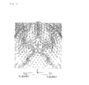
- Fig. 15 shows the results of computations of the intensity distribution within a crystal with a transmission mode of electromagnetic waves in the vicinity of 52 cm -1 .
- the intensity distribution is indicated by color density (actual color) in the figure, with dark colored portions (actual red) indicating the greatest intensity on the scale indicated beneath the graph.
- the computational results of the intensity distribution shown in Fig. 15 indicate that electromagnetic radiation near 52 cm -1 propagated along the optical waveguide path in the form of the defect region.
- the transmitted spectrum at SL2 was computed taking the structure shown in Fig. 9, in which multiple columns were removed from the structure shown in Fig. 7 to form a branching defect region, as the computational model. Specifically, a total of 28 rods were removed from positions on three of the five rotation symmetry axes in the five-rotation symmetry arrangement shown in Fig. 7 to form defect regions. It was assumed that SL0 was irradiated with light corresponding to millimeter-waves (frequencies of from 0 to 200 cm -1 ), and spectrum of transmitted light reaching position SL2 was calculated. The results are given in Fig. 16. The results of the calculation of the intensity distribution within a crystal of that transmission mode are given in Fig. 17.
- a transmission mode was present in the vicinity of 52 cm -1 in Fig. 16.
- Fig. 17 showing the intensity distribution within a crystal of that transmission mode, indicates that electromagnetic radiation entering at SL0 branched evenly, reaching SL2 and SL4.
- the above-described embodiments have described the use of the photonic crystal of the present invention in defect waveguides.
- the photonic crystal of the present invention may also be employed in coupled cavity waveguides.
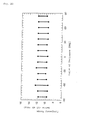
- the structure shown in Fig. 18 was fabricated.
- the structure shown in Fig. 18 was comprised of air (refractive index 1.0) and multiple acrylic rods (refractive index 1.61) and had a two-dimensional periodicity with five-rotation symmetry in the x-y plane, and could be assumed to have a shape that was infinite in the z direction.
- R denotes the radius, given by the spacing of the acrylic rods multiplied by N.
- the actual spacing of the acrylic rods was 12 mm.
- N corresponds to the number of concentric circles, and is an integer of from 0 to 20.
- n denotes the number of rods (from 1 to 5) on a single radius (R).
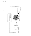
- Fig. 20 gives the spectrum of the electric field intensity detected with this test system.
- Fig. 20 is a graph showing the measurement results in which the electric field intensity is plotted on the y-axis and the frequency is plotted on the x-axis. In the graph, two sets of measurement results are superimposed.
- Fig. 20 reveals that within this structure, the electric field intensity was reduced sharply in a zone centered on 12 GHz. That is, the structure of Fig. 18 was found to be a photonic crystal with a photonic band gap present.
- a computation model of the photonic crystal shown in Fig. 18 was employed to calculate the intensity of light entering at various positions in the photonic crystal by the same method used to derive the computation results given in Fig. 4.
- the refractive index of the rods was 1.92
- the radius of the rods was 11 micrometers
- the distance between rods was 85 micrometers.
- the refractive index of the rods was made 1.61
- the radius of the rods was made 3 mm
- the distance between rods was made 12 mm.
- Fig. 22 is a graph showing that when the entry direction was changed from 0 to 90°, the intensity dropped to below -10 dB, that is, it is a graph showing the frequency range in which the photonic band gap was present.
- the structure of Fig. 7 exhibited nearly identical photonic band gap frequencies even when the angle of light incidence was varied.
- photonic crystal fabricated in the embodiment a band gap for light on the millimeter-wave level has been disclosed.
- photonic crystals exhibiting a photonic band gap for light at wavelengths within the infrared to visible range are photonic crystals exhibiting a photonic band gap for light at wavelengths within the infrared to visible range.
- Photonic crystals corresponding to light in the infrared to visible range can by fabricated by machining holes in the above-described semiconductor and forming multiple rods comprised of air in the semiconductor at multiple positions having two-dimensional rotational symmetry.
- a photonic crystal thus fabricated can be presumed to exhibit the same good characteristics as demonstrated by the present embodiment.
- the present invention provides a novel photonic crystal in which is formed a full photonic band gap capable of blocking light in all directions of propagation.
- the present invention further provides a novel photonic crystal without directional dependence of the photonic band gap.
- the present invention provides a novel photonic crystal permitting a reduction in restrictions on the selection and fabrication of constituent materials.
- the present invention provides an optical waveguide element affording little loss of light and reducing the limits on the direction of bending of the propagation path of the light.
- the present invention provides an optical waveguide element broadening the scope of freedom in the design of optical circuits when applied to optical circuits.
Landscapes
- Engineering & Computer Science (AREA)
- Physics & Mathematics (AREA)
- Optics & Photonics (AREA)
- Chemical & Material Sciences (AREA)
- Nanotechnology (AREA)
- Microelectronics & Electronic Packaging (AREA)
- General Physics & Mathematics (AREA)
- Life Sciences & Earth Sciences (AREA)
- Biophysics (AREA)
- Crystallography & Structural Chemistry (AREA)
- Optical Integrated Circuits (AREA)
Abstract
Description
Claims (10)
- A photonic crystal having a structure of which the refractive index changes with a periodicity defined in a polar coordinate system.
- The photonic crystal of claim 1, in which refractive index changes between two values of n1 and n2 (where n1 is not equal to n2) based on a periodicity defined in a polar coordinate system.
- The photonic crystal of claim 1 or 2, wherein said periodicity is of a non-translational symmetry.
- The photonic crystal of any one of claims 1-3, wherein said periodicity has a rotational symmetry.
- The photonic crystal of any one of claims 1-4, wherein the refractive index changes based on a periodicity that is two-dimensionally defined in a polar coordinate system.
- The photonic crystal of any one of claims 1-5, in which a structural unit comprising a first material having a refractive index of n1 and a second material having a refractive index of n2 (where n1 is not equal to n2) repeatedly occurs at positions rotated by a degree (0<<<360) about a point serving as the center of a polar coordinate system.
- The photonic crystal of any one of claim 1, in which a region having a refractive index differing from air in space is arranged with a periodicity defined by a polar coordinate system.
- A photonic crystal comprising plural elements with a refractive index n1, arranged in a two-dimensional rotational symmetry lattice; and plural spaces with a refractive index n2 (where n1 is not equal to n2) between adjacent said elements.
- An optical waveguide element comprising a photonic crystal of any one of claims 1-8, and a defect region of incomplete photonic crystal periodicity formed within said photonic crystal, wherein said defect region functions as an optical waveguide path by guiding from said inlet region to said outlet region an optical signal incapable of propagating through the photonic band gap of said photonic crystal.
- The optical waveguide element of claim 9, wherein said defect region comprises at least one bend in the direction of light propagation, or at least one region lying in a circular arc in the direction of light propagation.
Applications Claiming Priority (4)
| Application Number | Priority Date | Filing Date | Title |
|---|---|---|---|
| JP2001252384 | 2001-08-23 | ||
| JP2001252384 | 2001-08-23 | ||
| JP2002237058 | 2002-08-15 | ||
| JP2002237058A JP3743637B2 (en) | 2001-08-23 | 2002-08-15 | Photonic crystal and optical waveguide element |
Publications (2)
| Publication Number | Publication Date |
|---|---|
| EP1312947A2 true EP1312947A2 (en) | 2003-05-21 |
| EP1312947A3 EP1312947A3 (en) | 2004-03-31 |
Family
ID=26620840
Family Applications (1)
| Application Number | Title | Priority Date | Filing Date |
|---|---|---|---|
| EP02255907A Withdrawn EP1312947A3 (en) | 2001-08-23 | 2002-08-23 | Photonic crystal and optical waveguide elements |
Country Status (3)
| Country | Link |
|---|---|
| US (2) | US7113319B2 (en) |
| EP (1) | EP1312947A3 (en) |
| JP (1) | JP3743637B2 (en) |
Families Citing this family (14)
| Publication number | Priority date | Publication date | Assignee | Title |
|---|---|---|---|---|
| US7385177B2 (en) * | 2005-01-05 | 2008-06-10 | Ramot At Tel-Aviv University Ltd. | Light guide rotation rate detector with coupled optical resonators |
| US7332697B2 (en) | 2005-12-23 | 2008-02-19 | National Research Council Of Canada | Photonic bandgap reflector-suppressor |
| JP5063139B2 (en) | 2007-02-27 | 2012-10-31 | 日本航空電子工業株式会社 | Photonic structure |
| JP5008131B2 (en) * | 2007-03-26 | 2012-08-22 | 独立行政法人産業技術総合研究所 | Optical waveguide and optical device apparatus |
| JP4795289B2 (en) * | 2007-03-26 | 2011-10-19 | 独立行政法人産業技術総合研究所 | Optical device apparatus having coupled optical waveguide |
| WO2009044715A1 (en) * | 2007-10-01 | 2009-04-09 | Nec Corporation | Photonic crystal body |
| JP5365521B2 (en) * | 2007-10-01 | 2013-12-11 | 日本電気株式会社 | Photonic crystal |
| JP5365520B2 (en) * | 2007-10-01 | 2013-12-11 | 日本電気株式会社 | Photonic crystal |
| EP2445986A4 (en) * | 2009-06-22 | 2017-09-13 | The Trustees Of Princeton University | Non-crystalline materials having complete photonic, electronic, or phononic band gaps |
| TWI412551B (en) | 2010-08-25 | 2013-10-21 | Univ Nat Cheng Kung | Manufacturing method of polymer film with photonic crystal structure |
| TWI543386B (en) * | 2011-03-28 | 2016-07-21 | 財團法人工業技術研究院 | Circular photonic crystal structure, light emitting diode element, and photoelectric conversion element |
| CN102784436B (en) * | 2011-05-16 | 2015-04-29 | 深圳光启高等理工研究院 | Microwave hyperthermia therapy radiator and microwave hyperthermia therapy device |
| WO2012149824A1 (en) * | 2011-04-30 | 2012-11-08 | 深圳光启高等理工研究院 | Antenna based on metamaterial, microwave thermal therapy radiator, and microwave thermal therapy device |
| CN114996992B (en) * | 2022-05-07 | 2024-06-21 | 华中科技大学 | A method and system for solving eigenmodes of rotationally symmetric optical devices |
Family Cites Families (8)
| Publication number | Priority date | Publication date | Assignee | Title |
|---|---|---|---|---|
| JPH08505707A (en) | 1993-01-08 | 1996-06-18 | マサチユセツツ・インスチチユート・オブ・テクノロジー | Low loss light and optoelectronic integrated circuits |
| US5585968A (en) * | 1993-12-01 | 1996-12-17 | International Business Machines Corporation | Optical elements having regions of different indices of refraction and method of fabricating the same |
| EP1385028A1 (en) | 1999-02-19 | 2004-01-28 | Blazephotonics Limited | Improvements in or relating to photonic crystal fibres |
| JP2001252384A (en) | 2000-03-10 | 2001-09-18 | Miyuki:Kk | Hole in one game machine |
| JP3923244B2 (en) * | 2000-09-01 | 2007-05-30 | 富士フイルム株式会社 | Optical element |
| JP2002098916A (en) * | 2000-09-26 | 2002-04-05 | Hamamatsu Photonics Kk | Optical device |
| US6859304B2 (en) * | 2002-08-09 | 2005-02-22 | Energy Conversion Devices, Inc. | Photonic crystals and devices having tunability and switchability |
| US6775448B2 (en) * | 2002-11-05 | 2004-08-10 | Mesophotonics Limited | Optical device |
-
2002
- 2002-08-15 JP JP2002237058A patent/JP3743637B2/en not_active Expired - Fee Related
- 2002-08-22 US US10/225,156 patent/US7113319B2/en not_active Expired - Fee Related
- 2002-08-23 EP EP02255907A patent/EP1312947A3/en not_active Withdrawn
-
2004
- 2004-11-30 US US10/998,899 patent/US6941055B2/en not_active Expired - Fee Related
Also Published As
| Publication number | Publication date |
|---|---|
| JP3743637B2 (en) | 2006-02-08 |
| JP2003139978A (en) | 2003-05-14 |
| US20030053790A1 (en) | 2003-03-20 |
| US7113319B2 (en) | 2006-09-26 |
| US20050100299A1 (en) | 2005-05-12 |
| US6941055B2 (en) | 2005-09-06 |
| EP1312947A3 (en) | 2004-03-31 |
Similar Documents
| Publication | Publication Date | Title |
|---|---|---|
| US7113319B2 (en) | Photonic crystal and optical waveguide elements | |
| EP1606660B1 (en) | Polarization splitting grating couplers | |
| US7339539B2 (en) | Photonic crystal exhibiting negative refraction without requiring a negative effective index | |
| US5990850A (en) | Metallodielectric photonic crystal | |
| US8780010B2 (en) | Metamaterial provided with at least one spiral conductor for propagating electromagnetic wave | |
| US20230221463A1 (en) | Metasurface optical device covered with reflective layer, optical apparatus and manufacturing method | |
| US20120327666A1 (en) | Metamaterial for deflecting electromagnetic wave | |
| KR100877132B1 (en) | Design method and computer program of planar optical circuit and wave propagation circuit | |
| CN216670309U (en) | Supersurface optical device and optical apparatus with tilted nanostructure elements | |
| US20160238787A1 (en) | Forked grating coupler | |
| CN116324548A (en) | Optical Phased Array Setup for LIDAR Sensors | |
| US6904200B2 (en) | Multidimensional optical gratings | |
| US7136561B2 (en) | Two-dimensional photonic crystal, and waveguide and resonator using the same | |
| US7447411B2 (en) | Photonic structure | |
| US8729511B2 (en) | Electromagnetic wave beam splitter | |
| WO2006124962A2 (en) | Photonic crystal devices using negative refraction | |
| JP2003131028A (en) | Optical circuit | |
| Wu et al. | Broadband optical negative refraction based on dielectric phase gradient metagratings | |
| RU2284062C2 (en) | Electromagnetic radiation structuring device | |
| Prather et al. | Dispersion engineering of photonic crystals | |
| CN117769679A (en) | An optical antenna for an optical phase antenna array | |
| Howley et al. | Polymer waveguides and thermo-optic switches for an optical true time delay phased array antenna | |
| Zengerle | Photonic Crystal Waveguides: Dispersion, Anomalous Refraction and Applications | |
| Noda et al. | Three-dimensional photonic crystals |
Legal Events
| Date | Code | Title | Description |
|---|---|---|---|
| PUAI | Public reference made under article 153(3) epc to a published international application that has entered the european phase |
Free format text: ORIGINAL CODE: 0009012 |
|
| AK | Designated contracting states |
Designated state(s): AT BE BG CH CY CZ DE DK EE ES FI FR GB GR IE IT LI LU MC NL PT SE SK TR |
|
| AX | Request for extension of the european patent |
Extension state: AL LT LV MK RO SI |
|
| PUAL | Search report despatched |
Free format text: ORIGINAL CODE: 0009013 |
|
| AK | Designated contracting states |
Kind code of ref document: A3 Designated state(s): AT BE BG CH CY CZ DE DK EE ES FI FR GB GR IE IT LI LU MC NL PT SE SK TR |
|
| AX | Request for extension of the european patent |
Extension state: AL LT LV MK RO SI |
|
| 17P | Request for examination filed |
Effective date: 20040914 |
|
| AKX | Designation fees paid |
Designated state(s): AT BE BG CH CY CZ DE DK EE ES FI FR GB GR IE IT LI LU MC NL PT SE SK TR |
|
| 17Q | First examination report despatched |
Effective date: 20060104 |
|
| GRAP | Despatch of communication of intention to grant a patent |
Free format text: ORIGINAL CODE: EPIDOSNIGR1 |
|
| STAA | Information on the status of an ep patent application or granted ep patent |
Free format text: STATUS: THE APPLICATION IS DEEMED TO BE WITHDRAWN |
|
| 18D | Application deemed to be withdrawn |
Effective date: 20080722 |