EP1312443B1 - Method of levelling depressed surfaces of organic crystals - Google Patents
Method of levelling depressed surfaces of organic crystals Download PDFInfo
- Publication number
- EP1312443B1 EP1312443B1 EP02257903A EP02257903A EP1312443B1 EP 1312443 B1 EP1312443 B1 EP 1312443B1 EP 02257903 A EP02257903 A EP 02257903A EP 02257903 A EP02257903 A EP 02257903A EP 1312443 B1 EP1312443 B1 EP 1312443B1
- Authority
- EP
- European Patent Office
- Prior art keywords
- probe
- depression
- levelling
- crystal
- organic
- Prior art date
- Legal status (The legal status is an assumption and is not a legal conclusion. Google has not performed a legal analysis and makes no representation as to the accuracy of the status listed.)
- Expired - Lifetime
Links
Images

Classifications
-
- B—PERFORMING OPERATIONS; TRANSPORTING
- B24—GRINDING; POLISHING
- B24B—MACHINES, DEVICES, OR PROCESSES FOR GRINDING OR POLISHING; DRESSING OR CONDITIONING OF ABRADING SURFACES; FEEDING OF GRINDING, POLISHING, OR LAPPING AGENTS
- B24B1/00—Processes of grinding or polishing; Use of auxiliary equipment in connection with such processes
Definitions
- the present invention relates to a method as per the preamble of claim 1.
- An example of such a method is disclosed by JP 2001 105 285 A .
- organic crystals used as a non-linear optical material are usually single crystals, it is necessary to fill the defective surface depression with a filling material of the same kind as the single crystal body so as to minimize the loss in the requisite properties such as laser beam incidence and energy transducing efficiency at the interface between the filling of the depression and the base body of the single crystal.
- Japanese Patent Kokai 4-1951 proposes application of the Langmuir-Blodgett method (referred to as the LB method hereinafter) to the preparation of an organic thin film having a smooth surface with roughness of 1 nm or less.
- This method is not suitable for levelling of molecular-order scratches or depressions such as molecular defects.
- the present invention has an object to provide a method for obtaining an organic crystal for use as a non-linear optical material having a fully smoothened surface so as to be free from a decrease in the laser beam incidence or energy transducing efficiency by locally levelling a scratch or pit as a defective depression in a novel method capable of accomplishing an ultimate smooth surface with molecular scale flatness.
- the present invention provides a method for the preparation of an organic crystal having a fully smoothened surface which comprises the steps of:
- the thus treated surface of the crystal is extremely flat since the surface roughness is far below the molecular step height which is 0.89 nm.
- Figures 1A, 1B, 1C and 1D are each a microscopic photograph of the surface of an organic crystal in the course of a levelling treatment of surface depressions carried out in Example 1.
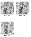
- Figures 2A, 2B and 2C are each a microscopic photograph of the surface of an organic crystal in the course of a levelling treatment of a depression carried out in Example 2.
- the method of the present invention for local levelling of a defective depression in the surface of an organic crystal used as a non-linear optical material is applicable to single crystals of a variety of organic compounds without particular limitations but the method would be most successful when the crystal is of an organic compound selected from 4-dimethylaminostilbazolium salts, L-arginine phosphates, 4-nitroaniline, 2-methyl-4-nitroaniline, 2-methyl-4-nitro-N-methylaniline, 3-acetamido-4-dimethylamino nitro-benzene, N-(5-nitro-2-pyridyl)-5-prolinol, and N,N-dimethylamino-nitrostilbene.
- organic crystals are generally soft and weak as compared with most inorganic crystals so that, even if the crystal has once been imparted with a fully smoothened surface, the surface is liable to be damaged by a thermal or mechanical shock or by receiving a chemical attack from outside forming a defective depression.
- the objective body to which the inventive method is applicable is not limited to isolated single crystals of the above named organic compounds but the method is applicable to a coating layer formed on a variety of substrates such as metal plates, glass plates and ceramic plates by a conventional film-forming method such as the vacuum vapor deposition method and chemical vapor-phase deposition (CVD) method and also to an accumulated multilayered film formed by the LB method.
- a conventional film-forming method such as the vacuum vapor deposition method and chemical vapor-phase deposition (CVD) method and also to an accumulated multilayered film formed by the LB method.
- the inventive method for levelling of a defective depression in the surface of an organic crystal is conducted by two-dimensionally scanning the surface on and around the depression with a probe to shave off the circumferential portions around the depression forming shavings and then transferring the shavings into the depression so as to fill the depression with the shavings up to the same level as the flat surface around the depression.
- the probe used in the inventive method it is convenient to divertedly employ a probe equipped in an atomic force microscope if the probe tip of the probe has an appropriate radius of curvature although the probe is not particularly limitative provided that the contacting load to the crystal surface can be adequately controlled within the specified range.
- the probe tip of the probe to be contacted with the crystal surface has a radius of curvature in the range from 1 nm to 100 nm or, preferably, from 5 nm to 40 nm.
- the contacting load on the probe during surface scanning should be controlled in the range from 1 nN to 100 nN or, preferably, from 5 nN to 30 nN.
- shaving of the crystal surface cannot be complete while, when the radius of curvature is too large, the surface formed by shaving cannot be imparted with molecular level smoothness.
- the contacting load on the probe is too small, shaving of the surface can hardly be carried out with smoothness while, when the contacting load is too large, shaving of the surface sometimes proceeds too much so as not to give a fully smoothened surface as desired.
- the organic crystal subjected to the surface levelling treatment according to the inventive method was a single crystal of 4-(4-dimethylaminostyryl)-1-methylpyridinium tosylate (referred to as DAST hereinafter) having a stepped structure as shown in the photograph of Figure 1A, of which a crystallographic (001) surface of molecular-level flatness had three pit-like defective depressions as indicated in the photograph of Figure 1B including Pit 1 having a length of 72 nm and depth of 0.70 nm, Pit 2 having a length of 35 nm and depth of 0.74 nm and Pit 3 having a length of 45 nm and depth of 0.59 nm.
- DAST 4-(4-dimethylaminostyryl)-1-methylpyridinium tosylate
- a 600 nm by 600 nm square area of the crystal surface including these three pits was scanned two-dimensionally with a probe of an atomic force microscope, of which the probe tip had a radius of curvature of 20 nm, by the contact method under a vertical contacting load of 14 nN to find levelling of the Pit 3 after only 3 scans (see Figure 1C) and levelling of the Pits 1 and 2 after 8 scans (see Figure 1D).
- this DAST crystal had a stepped structure of 0.9 nm corresponding to the thickness of the DAST ion pair and the flat portion thereof had a terrace-formed configuration. It was indicated therefore that the defective depressions found there could be levelled to impart molecular level smoothness to the flat terrace or, namely, a possibility was indicated for molecular-level levelling of depressions.
- the thus treated surface was extremely flat since the surface roughness was far below the molecular step height which was 0.89 nm.
- the center line-average surface roughness Ra of the crystal surface shown in Figure 1B was decreased from 0.11 nm to 0.05 nm.
- the crystallographic (001) surface of a DAST single crystal with a roughness Rmax of 5.4 nm to be subjected to the levelling treatment had a pit-like defective depression of 109 nm length and 5.4 nm depth as indicated by the arrow in Figure 2A.
- the procedure for the levelling treatment was substantially the same as in Example 1 except that the vertical contacting load on the probe was 19 nN instead of 14 nN and scanning was conducted on a 1110 nm by 1110 nm square area including the pit.
- the depth of the pit was decreased to 2.5 nm after 4 repeated scans (see Figure 2B) and the pit disappeared completely after 10 repeated scans (see Figure 2C).
- the center line-average surface roughness Ra of 0.31 nm before the levelling treatment remained unchanged by this treatment.
- the thus levelling-treated area of the crystal surface had a roughness about equivalent to the surface rough-ness of the base surface therearound.
- Example 2 The same experimental procedure as in Example 2 was undertaken except for an increase of the contacting load on the probe from 19 nN to 130 nN. The results were that shaving of the crystal surface took place at unlimited portions of the surface including the depression so that the treated surface was coarse with undulation and had a surface roughness Ra of 50 nm.
Landscapes
- Engineering & Computer Science (AREA)
- Mechanical Engineering (AREA)
- Crystals, And After-Treatments Of Crystals (AREA)
- Surface Treatment Of Optical Elements (AREA)
- Optical Modulation, Optical Deflection, Nonlinear Optics, Optical Demodulation, Optical Logic Elements (AREA)
- ing And Chemical Polishing (AREA)
- Treatments Of Macromolecular Shaped Articles (AREA)
Description
- The present invention relates to a method as per the preamble of claim 1. An example of such a method is disclosed by
JP 2001 105 285 A - It is a well established technology to utilize certain crystalline materials as a non-linear optical material. It is essential in this technology to ensure perfect flatness or smoothness of the crystal surface in a molecular level flatness in order to minimize the loss in the laser beam incidence and energy transducing efficiency inherent in the crystalline material per se. As compared with inorganic crystals, organic crystals in general have a fairly low surface hardness and are sometimes liable to occurrence of surface defects such as scratches and pits resulting in a loss of the optical properties inherent in the crystalline material.
- It is therefore desirable for such an organic crystal having a depressive surface defect that the depression is efficiently levelled to recover molecular-level smoothness of the crystal surface. Since the organic crystals used as a non-linear optical material are usually single crystals, it is necessary to fill the defective surface depression with a filling material of the same kind as the single crystal body so as to minimize the loss in the requisite properties such as laser beam incidence and energy transducing efficiency at the interface between the filling of the depression and the base body of the single crystal.
- Several methods are proposed in the prior art for levelling a defective depressed surface of a relatively soft and weak non-linear optical material such as certain organic crystals including a method of mechanical polishing of the whole surface as disclosed in
Japanese Patent Kokai 5-309560 Japanese Patent Kokai 5-285827 -
Japanese Patent Kokai 4-1951 - The inventors previously proposed (
Japanese Patent Kokai 2001-105285 - Thus, it is the present status of the art that no efficient method is known for local levelling of a scratch or a pit subsequently produced on the surface of an organic crystal once levelled in a molecular level or obtained by whole-surface polishing.
- In view of the above described problems and disadvantages in the prior art, the present invention has an object to provide a method for obtaining an organic crystal for use as a non-linear optical material having a fully smoothened surface so as to be free from a decrease in the laser beam incidence or energy transducing efficiency by locally levelling a scratch or pit as a defective depression in a novel method capable of accomplishing an ultimate smooth surface with molecular scale flatness.
- Thus, the present invention provides a method for the preparation of an organic crystal having a fully smoothened surface which comprises the steps of:
- (a) bringing a probe at a probe tip thereof having a radius of curvature in the range from 1 nm to 100 nm into contact with the surface of an organic crystal having a depression under a contacting load in the range from 1 nN to 100 nN;
- (b) two-dimensionally scanning the surface with the probe under the contacting load to shave off the circumferential portions of the crystal around the depression forming shavings; and
- (c) transferring the shavings into the depression to fill the depression therewith up to a level flush with the surface level around the depression.
- The thus treated surface of the crystal is extremely flat since the surface roughness is far below the molecular step height which is 0.89 nm.
- In the drawings: Figures 1A, 1B, 1C and 1D are each a microscopic photograph of the surface of an organic crystal in the course of a levelling treatment of surface depressions carried out in Example 1.
- Figures 2A, 2B and 2C are each a microscopic photograph of the surface of an organic crystal in the course of a levelling treatment of a depression carried out in Example 2.
- The method of the present invention for local levelling of a defective depression in the surface of an organic crystal used as a non-linear optical material is applicable to single crystals of a variety of organic compounds without particular limitations but the method would be most successful when the crystal is of an organic compound selected from 4-dimethylaminostilbazolium salts, L-arginine phosphates, 4-nitroaniline, 2-methyl-4-nitroaniline, 2-methyl-4-nitro-N-methylaniline, 3-acetamido-4-dimethylamino nitro-benzene, N-(5-nitro-2-pyridyl)-5-prolinol, and N,N-dimethylamino-nitrostilbene.
- These organic crystals are generally soft and weak as compared with most inorganic crystals so that, even if the crystal has once been imparted with a fully smoothened surface, the surface is liable to be damaged by a thermal or mechanical shock or by receiving a chemical attack from outside forming a defective depression.
- It is possible by properly undertaking the inventive method to effect full levelling of depressions having a maximum depth Rmax not exceeding 50 nm and a center line-average surface roughness Ra not exceeding 5 nm or, in particular, molecular level fine depressions having a maximum depth Rmax not exceeding 3 nm and a center line-average surface roughness Ra not exceeding 1 nm.
- The objective body to which the inventive method is applicable is not limited to isolated single crystals of the above named organic compounds but the method is applicable to a coating layer formed on a variety of substrates such as metal plates, glass plates and ceramic plates by a conventional film-forming method such as the vacuum vapor deposition method and chemical vapor-phase deposition (CVD) method and also to an accumulated multilayered film formed by the LB method.
- The inventive method for levelling of a defective depression in the surface of an organic crystal is conducted by two-dimensionally scanning the surface on and around the depression with a probe to shave off the circumferential portions around the depression forming shavings and then transferring the shavings into the depression so as to fill the depression with the shavings up to the same level as the flat surface around the depression.
- With regard to the probe used in the inventive method, it is convenient to divertedly employ a probe equipped in an atomic force microscope if the probe tip of the probe has an appropriate radius of curvature although the probe is not particularly limitative provided that the contacting load to the crystal surface can be adequately controlled within the specified range.
- It is important in the inventive method that the probe tip of the probe to be contacted with the crystal surface has a radius of curvature in the range from 1 nm to 100 nm or, preferably, from 5 nm to 40 nm. The contacting load on the probe during surface scanning should be controlled in the range from 1 nN to 100 nN or, preferably, from 5 nN to 30 nN. When a probe of which the probe tip has a radius of curvature smaller than 1 nm is used, shaving of the crystal surface cannot be complete while, when the radius of curvature is too large, the surface formed by shaving cannot be imparted with molecular level smoothness. When the contacting load on the probe is too small, shaving of the surface can hardly be carried out with smoothness while, when the contacting load is too large, shaving of the surface sometimes proceeds too much so as not to give a fully smoothened surface as desired.
- It is necessary in the inventive method that scanning of the surface with the probe is conducted as many times as necessary until the defective depression on the surface is completely filled with the shavings produced by shaving of the circumferential area around the depression and then transferred into the depression. Scanning with the probe repeated 3 to about 20 times is sufficient in most cases though dependent on various factors including size and depth of the depression to be levelled, radius of curvature of the probe tip of the probe, contacting load on the probe during scanning and others. By properly conducting the inventive method, a defective depression formed on an organic crystal disappears almost completely so as to give an organic crystal of which the surface has molecular-level smoothness.
- In the following, the method of the present invention is described in more detail by way of Examples and a Comparative Example, which, however, never limit the scope of the invention in any way.
- The organic crystal subjected to the surface levelling treatment according to the inventive method was a single crystal of 4-(4-dimethylaminostyryl)-1-methylpyridinium tosylate (referred to as DAST hereinafter) having a stepped structure as shown in the photograph of Figure 1A, of which a crystallographic (001) surface of molecular-level flatness had three pit-like defective depressions as indicated in the photograph of Figure 1B including Pit 1 having a length of 72 nm and depth of 0.70 nm,
Pit 2 having a length of 35 nm and depth of 0.74 nm andPit 3 having a length of 45 nm and depth of 0.59 nm. - A 600 nm by 600 nm square area of the crystal surface including these three pits was scanned two-dimensionally with a probe of an atomic force microscope, of which the probe tip had a radius of curvature of 20 nm, by the contact method under a vertical contacting load of 14 nN to find levelling of the
Pit 3 after only 3 scans (see Figure 1C) and levelling of thePits 1 and 2 after 8 scans (see Figure 1D). - As is understood from Figure 1A, this DAST crystal had a stepped structure of 0.9 nm corresponding to the thickness of the DAST ion pair and the flat portion thereof had a terrace-formed configuration. It was indicated therefore that the defective depressions found there could be levelled to impart molecular level smoothness to the flat terrace or, namely, a possibility was indicated for molecular-level levelling of depressions. The thus treated surface was extremely flat since the surface roughness was far below the molecular step height which was 0.89 nm.
- By this levelling treatment, the center line-average surface roughness Ra of the crystal surface shown in Figure 1B was decreased from 0.11 nm to 0.05 nm.
- The crystallographic (001) surface of a DAST single crystal with a roughness Rmax of 5.4 nm to be subjected to the levelling treatment had a pit-like defective depression of 109 nm length and 5.4 nm depth as indicated by the arrow in Figure 2A. The procedure for the levelling treatment was substantially the same as in Example 1 except that the vertical contacting load on the probe was 19 nN instead of 14 nN and scanning was conducted on a 1110 nm by 1110 nm square area including the pit. By repeating the two-dimensional scanning with the probe, the depth of the pit was decreased to 2.5 nm after 4 repeated scans (see Figure 2B) and the pit disappeared completely after 10 repeated scans (see Figure 2C). The center line-average surface roughness Ra of 0.31 nm before the levelling treatment remained unchanged by this treatment. The thus levelling-treated area of the crystal surface had a roughness about equivalent to the surface rough-ness of the base surface therearound.
- The same experimental procedure as in Example 2 was undertaken except for an increase of the contacting load on the probe from 19 nN to 130 nN. The results were that shaving of the crystal surface took place at unlimited portions of the surface including the depression so that the treated surface was coarse with undulation and had a surface roughness Ra of 50 nm.
Claims (4)
- A method for the preparation of an organic single crystal having a surface with molecular-level smoothness which comprises the steps of:bringing a probe at a probe tip thereof having a radius of curvature in the range from 1 nm to 100 nm into contact with a surface of the organic single crystal having a depression under a contacting load in the range from 1 nN to 100 nN;two-dimensionally scanning the surface of the organic single crystal with the probe under the contacting load around the depression forming shavings; characterized bytransferring the shavings into the depression to fill the depression therewith up to a level flush with the surface level around the depression.
- The method according to claim 1 in which the probe tip of the probe has a radius of curvature in the range from 5 nm to 40 nm.
- The method according to claim 1 or claim 2 in which the contacting load on the probe is in the range from 5 nN to 30 nN.
- The method according to any one of claims 1 to 3 in which the two-dimensional scanning of the surface with the probe is repeated from 3 times to 20 times.
Applications Claiming Priority (2)
| Application Number | Priority Date | Filing Date | Title |
|---|---|---|---|
| JP2001351172 | 2001-11-16 | ||
| JP2001351172A JP3548804B2 (en) | 2001-11-16 | 2001-11-16 | Organic crystal surface defect repair method |
Publications (3)
| Publication Number | Publication Date |
|---|---|
| EP1312443A2 EP1312443A2 (en) | 2003-05-21 |
| EP1312443A3 EP1312443A3 (en) | 2003-09-24 |
| EP1312443B1 true EP1312443B1 (en) | 2007-06-13 |
Family
ID=19163517
Family Applications (1)
| Application Number | Title | Priority Date | Filing Date |
|---|---|---|---|
| EP02257903A Expired - Lifetime EP1312443B1 (en) | 2001-11-16 | 2002-11-15 | Method of levelling depressed surfaces of organic crystals |
Country Status (3)
| Country | Link |
|---|---|
| US (1) | US20030096502A1 (en) |
| EP (1) | EP1312443B1 (en) |
| JP (1) | JP3548804B2 (en) |
Family Cites Families (3)
| Publication number | Priority date | Publication date | Assignee | Title |
|---|---|---|---|---|
| US5210425A (en) * | 1991-08-30 | 1993-05-11 | E. I. Du Pont De Nemours And Company | Etching of nanoscale structures |
| US5252835A (en) * | 1992-07-17 | 1993-10-12 | President And Trustees Of Harvard College | Machining oxide thin-films with an atomic force microscope: pattern and object formation on the nanometer scale |
| JP2001105285A (en) * | 1999-10-05 | 2001-04-17 | Agency Of Ind Science & Technol | Method for producing organic ion crystal having smooth surface |
-
2001
- 2001-11-16 JP JP2001351172A patent/JP3548804B2/en not_active Expired - Lifetime
-
2002
- 2002-11-01 US US10/285,474 patent/US20030096502A1/en not_active Abandoned
- 2002-11-15 EP EP02257903A patent/EP1312443B1/en not_active Expired - Lifetime
Also Published As
| Publication number | Publication date |
|---|---|
| JP2003145500A (en) | 2003-05-20 |
| JP3548804B2 (en) | 2004-07-28 |
| US20030096502A1 (en) | 2003-05-22 |
| EP1312443A3 (en) | 2003-09-24 |
| EP1312443A2 (en) | 2003-05-21 |
Similar Documents
| Publication | Publication Date | Title |
|---|---|---|
| Komanduri | On material removal mechanisms in finishing of advanced ceramics and glasses | |
| DE69516035T2 (en) | Method for producing a semiconductor covered with hard material | |
| KR102300061B1 (en) | Method for combined laser treatment of solids to be separated | |
| EP2267189B1 (en) | High surface quality gan wafer and method of fabricating same | |
| US7531428B2 (en) | Recycling the reconditioned substrates for fabricating compound material wafers | |
| US5458827A (en) | Method of polishing and figuring diamond and other superhard material surfaces | |
| US4631804A (en) | Technique for reducing substrate warpage springback using a polysilicon subsurface strained layer | |
| Shibata et al. | Cross‐section transmission electron microscope observations of diamond‐turned single‐crystal Si surfaces | |
| JP4855254B2 (en) | Method for forming a thin layer of semiconductor material from a donor wafer having both sides | |
| US5500157A (en) | Method of shaping polycrystalline diamond | |
| JP2024022232A (en) | Diamond processing method and equipment | |
| US20210001429A1 (en) | Methods of using laser energy to remove particles from a surface | |
| Kim et al. | Nano periodic structure formation in 4H–SiC crystal using femtosecond laser double-pulses | |
| CN117359104A (en) | A chemical mechanical polishing method of silicon carbide crystal based on liquid phase laser technology | |
| EP1312443A2 (en) | Method of levelling depressed surfaces of organic crystals | |
| Mc Kay | Chemical Mechanical polishing and Direct Bonding of YAG and Y2O3 | |
| US5022957A (en) | Etching process for improving the strength of a laser-machined silicon-based ceramic article | |
| Tonnellier et al. | Wheel wear and surface/subsurface qualities when precision grinding optical materials | |
| EP3830321A1 (en) | Non-contact polishing of a crystalline layer or substrate by ion beam etching | |
| US20250229457A1 (en) | Rapid wafering of wide bandgap substrates | |
| Peng et al. | Atom-scale smoothing of monocrystalline silicon via non-abrasive catalytic polishing | |
| JP3250768B2 (en) | Method for forming diamond-like carbon film, method for manufacturing magnetic head, and method for manufacturing magnetic disk | |
| RU2855376C1 (en) | Method of femtosecond laser polishing of optical surfaces of nonlinear optical media | |
| WO2025190591A1 (en) | Heterostructure comprising a rough exposed portion of a support substrate | |
| Foecke et al. | Imaging of cracks in semiconductors using scanning tunneling microscopy |
Legal Events
| Date | Code | Title | Description |
|---|---|---|---|
| PUAI | Public reference made under article 153(3) epc to a published international application that has entered the european phase |
Free format text: ORIGINAL CODE: 0009012 |
|
| AK | Designated contracting states |
Designated state(s): AT BE BG CH CY CZ DE DK EE ES FI FR GB GR IE IT LI LU MC NL PT SE SK TR |
|
| AX | Request for extension of the european patent |
Extension state: AL LT LV MK RO SI |
|
| PUAL | Search report despatched |
Free format text: ORIGINAL CODE: 0009013 |
|
| RIC1 | Information provided on ipc code assigned before grant |
Ipc: 7B 24B 1/00 A Ipc: 7G 01B 7/34 B Ipc: 7G 02F 1/361 B |
|
| AK | Designated contracting states |
Kind code of ref document: A3 Designated state(s): AT BE BG CH CY CZ DE DK EE ES FI FR GB GR IE IT LI LU MC NL PT SE SK TR |
|
| AX | Request for extension of the european patent |
Extension state: AL LT LV MK RO SI |
|
| 17P | Request for examination filed |
Effective date: 20040202 |
|
| 17Q | First examination report despatched |
Effective date: 20040414 |
|
| AKX | Designation fees paid |
Designated state(s): FR GB |
|
| REG | Reference to a national code |
Ref country code: DE Ref legal event code: 8566 |
|
| GRAP | Despatch of communication of intention to grant a patent |
Free format text: ORIGINAL CODE: EPIDOSNIGR1 |
|
| GRAS | Grant fee paid |
Free format text: ORIGINAL CODE: EPIDOSNIGR3 |
|
| GRAA | (expected) grant |
Free format text: ORIGINAL CODE: 0009210 |
|
| AK | Designated contracting states |
Kind code of ref document: B1 Designated state(s): FR GB |
|
| REG | Reference to a national code |
Ref country code: GB Ref legal event code: FG4D |
|
| ET | Fr: translation filed | ||
| PLBE | No opposition filed within time limit |
Free format text: ORIGINAL CODE: 0009261 |
|
| STAA | Information on the status of an ep patent application or granted ep patent |
Free format text: STATUS: NO OPPOSITION FILED WITHIN TIME LIMIT |
|
| 26N | No opposition filed |
Effective date: 20080314 |
|
| PGFP | Annual fee paid to national office [announced via postgrant information from national office to epo] |
Ref country code: FR Payment date: 20101130 Year of fee payment: 9 |
|
| PGFP | Annual fee paid to national office [announced via postgrant information from national office to epo] |
Ref country code: GB Payment date: 20101118 Year of fee payment: 9 |
|
| GBPC | Gb: european patent ceased through non-payment of renewal fee |
Effective date: 20111115 |
|
| REG | Reference to a national code |
Ref country code: FR Ref legal event code: ST Effective date: 20120731 |
|
| PG25 | Lapsed in a contracting state [announced via postgrant information from national office to epo] |
Ref country code: GB Free format text: LAPSE BECAUSE OF NON-PAYMENT OF DUE FEES Effective date: 20111115 |
|
| PG25 | Lapsed in a contracting state [announced via postgrant information from national office to epo] |
Ref country code: FR Free format text: LAPSE BECAUSE OF NON-PAYMENT OF DUE FEES Effective date: 20111130 |